EP4398097A2 - Appareils, procédés et systèmes pour instructions de produit de point matriciel à virgule flottante à 8 bits - Google Patents
Appareils, procédés et systèmes pour instructions de produit de point matriciel à virgule flottante à 8 bits Download PDFInfo
- Publication number
- EP4398097A2 EP4398097A2 EP24177816.6A EP24177816A EP4398097A2 EP 4398097 A2 EP4398097 A2 EP 4398097A2 EP 24177816 A EP24177816 A EP 24177816A EP 4398097 A2 EP4398097 A2 EP 4398097A2
- Authority
- EP
- European Patent Office
- Prior art keywords
- floating point
- matrix
- bit floating
- data elements
- instruction
- Prior art date
- Legal status (The legal status is an assumption and is not a legal conclusion. Google has not performed a legal analysis and makes no representation as to the accuracy of the status listed.)
- Pending
Links
Images
















Classifications
-
- G—PHYSICS
- G06—COMPUTING OR CALCULATING; COUNTING
- G06F—ELECTRIC DIGITAL DATA PROCESSING
- G06F9/00—Arrangements for program control, e.g. control units
- G06F9/06—Arrangements for program control, e.g. control units using stored programs, i.e. using an internal store of processing equipment to receive or retain programs
- G06F9/30—Arrangements for executing machine instructions, e.g. instruction decode
- G06F9/30003—Arrangements for executing specific machine instructions
- G06F9/30007—Arrangements for executing specific machine instructions to perform operations on data operands
- G06F9/3001—Arithmetic instructions
- G06F9/30014—Arithmetic instructions with variable precision
-
- G—PHYSICS
- G06—COMPUTING OR CALCULATING; COUNTING
- G06F—ELECTRIC DIGITAL DATA PROCESSING
- G06F9/00—Arrangements for program control, e.g. control units
- G06F9/06—Arrangements for program control, e.g. control units using stored programs, i.e. using an internal store of processing equipment to receive or retain programs
- G06F9/30—Arrangements for executing machine instructions, e.g. instruction decode
- G06F9/38—Concurrent instruction execution, e.g. pipeline or look ahead
- G06F9/3885—Concurrent instruction execution, e.g. pipeline or look ahead using a plurality of independent parallel functional units
- G06F9/3887—Concurrent instruction execution, e.g. pipeline or look ahead using a plurality of independent parallel functional units controlled by a single instruction for multiple data lanes [SIMD]
-
- G—PHYSICS
- G06—COMPUTING OR CALCULATING; COUNTING
- G06F—ELECTRIC DIGITAL DATA PROCESSING
- G06F17/00—Digital computing or data processing equipment or methods, specially adapted for specific functions
- G06F17/10—Complex mathematical operations
- G06F17/16—Matrix or vector computation, e.g. matrix-matrix or matrix-vector multiplication, matrix factorization
-
- G—PHYSICS
- G06—COMPUTING OR CALCULATING; COUNTING
- G06F—ELECTRIC DIGITAL DATA PROCESSING
- G06F7/00—Methods or arrangements for processing data by operating upon the order or content of the data handled
- G06F7/38—Methods or arrangements for performing computations using exclusively denominational number representation, e.g. using binary, ternary, decimal representation
- G06F7/48—Methods or arrangements for performing computations using exclusively denominational number representation, e.g. using binary, ternary, decimal representation using non-contact-making devices, e.g. tube, solid state device; using unspecified devices
- G06F7/499—Denomination or exception handling, e.g. rounding or overflow
- G06F7/49905—Exception handling
- G06F7/4991—Overflow or underflow
- G06F7/49915—Mantissa overflow or underflow in handling floating-point numbers
-
- G—PHYSICS
- G06—COMPUTING OR CALCULATING; COUNTING
- G06F—ELECTRIC DIGITAL DATA PROCESSING
- G06F9/00—Arrangements for program control, e.g. control units
- G06F9/06—Arrangements for program control, e.g. control units using stored programs, i.e. using an internal store of processing equipment to receive or retain programs
- G06F9/30—Arrangements for executing machine instructions, e.g. instruction decode
- G06F9/30003—Arrangements for executing specific machine instructions
- G06F9/30007—Arrangements for executing specific machine instructions to perform operations on data operands
-
- G—PHYSICS
- G06—COMPUTING OR CALCULATING; COUNTING
- G06F—ELECTRIC DIGITAL DATA PROCESSING
- G06F9/00—Arrangements for program control, e.g. control units
- G06F9/06—Arrangements for program control, e.g. control units using stored programs, i.e. using an internal store of processing equipment to receive or retain programs
- G06F9/30—Arrangements for executing machine instructions, e.g. instruction decode
- G06F9/30003—Arrangements for executing specific machine instructions
- G06F9/30007—Arrangements for executing specific machine instructions to perform operations on data operands
- G06F9/30025—Format conversion instructions, e.g. Floating-Point to Integer, decimal conversion
-
- G—PHYSICS
- G06—COMPUTING OR CALCULATING; COUNTING
- G06F—ELECTRIC DIGITAL DATA PROCESSING
- G06F9/00—Arrangements for program control, e.g. control units
- G06F9/06—Arrangements for program control, e.g. control units using stored programs, i.e. using an internal store of processing equipment to receive or retain programs
- G06F9/30—Arrangements for executing machine instructions, e.g. instruction decode
- G06F9/30003—Arrangements for executing specific machine instructions
- G06F9/30007—Arrangements for executing specific machine instructions to perform operations on data operands
- G06F9/30036—Instructions to perform operations on packed data, e.g. vector, tile or matrix operations
-
- G—PHYSICS
- G06—COMPUTING OR CALCULATING; COUNTING
- G06F—ELECTRIC DIGITAL DATA PROCESSING
- G06F9/00—Arrangements for program control, e.g. control units
- G06F9/06—Arrangements for program control, e.g. control units using stored programs, i.e. using an internal store of processing equipment to receive or retain programs
- G06F9/30—Arrangements for executing machine instructions, e.g. instruction decode
- G06F9/30003—Arrangements for executing specific machine instructions
- G06F9/30007—Arrangements for executing specific machine instructions to perform operations on data operands
- G06F9/30036—Instructions to perform operations on packed data, e.g. vector, tile or matrix operations
- G06F9/30038—Instructions to perform operations on packed data, e.g. vector, tile or matrix operations using a mask
-
- G—PHYSICS
- G06—COMPUTING OR CALCULATING; COUNTING
- G06F—ELECTRIC DIGITAL DATA PROCESSING
- G06F9/00—Arrangements for program control, e.g. control units
- G06F9/06—Arrangements for program control, e.g. control units using stored programs, i.e. using an internal store of processing equipment to receive or retain programs
- G06F9/30—Arrangements for executing machine instructions, e.g. instruction decode
- G06F9/30181—Instruction operation extension or modification
- G06F9/30196—Instruction operation extension or modification using decoder, e.g. decoder per instruction set, adaptable or programmable decoders
-
- G—PHYSICS
- G06—COMPUTING OR CALCULATING; COUNTING
- G06F—ELECTRIC DIGITAL DATA PROCESSING
- G06F9/00—Arrangements for program control, e.g. control units
- G06F9/06—Arrangements for program control, e.g. control units using stored programs, i.e. using an internal store of processing equipment to receive or retain programs
- G06F9/30—Arrangements for executing machine instructions, e.g. instruction decode
- G06F9/38—Concurrent instruction execution, e.g. pipeline or look ahead
- G06F9/3885—Concurrent instruction execution, e.g. pipeline or look ahead using a plurality of independent parallel functional units
- G06F9/3888—Concurrent instruction execution, e.g. pipeline or look ahead using a plurality of independent parallel functional units controlled by a single instruction for multiple threads [SIMT] in parallel
-
- G—PHYSICS
- G06—COMPUTING OR CALCULATING; COUNTING
- G06N—COMPUTING ARRANGEMENTS BASED ON SPECIFIC COMPUTATIONAL MODELS
- G06N3/00—Computing arrangements based on biological models
- G06N3/02—Neural networks
- G06N3/06—Physical realisation, i.e. hardware implementation of neural networks, neurons or parts of neurons
- G06N3/063—Physical realisation, i.e. hardware implementation of neural networks, neurons or parts of neurons using electronic means
Definitions
- the disclosure relates generally to computer processor architecture, and, more specifically, to systems and methods for performing 8-bit floating-point matrix dot product instructions.
- Deep Learning is a class of machine learning algorithms. Deep learning architectures, such as deep neural networks, have been applied to fields including computer vision, speech recognition, natural language processing, audio recognition, social network filtering, machine translation, bioinformatics and drug design.
- Matrix-matrix multiplication (a.k.a., GEMM or General Matrix Multiplication) is a common compute-heavy operation on modern processors.
- Special hardware for matrix multiplication e.g., GEMM
- GEMM is a good option for improving the peak compute (and energy efficiency) of certain applications, such as deep learning.
- Some of these applications can operate on input data elements with relatively few bits without losing accuracy, as long as the output elements have enough bits (i.e., more than the inputs).
- handling matrices is a difficult and/or instruction intensive task. For example, rows of a matrix could be put into a plurality of packed data (e.g., SIMD or vector) registers and then operated on individually. For example, an add two 8x2 matrices may require a load or gather into four packed data registers depending upon data sizes. Then a first add of packed data registers corresponding to a first row from each matrix is performed and a second add of packed data registers corresponding to a second row from each matrix is performed. Then the resulting packed data registers are scattered back to memory. While for small matrices this scenario may be acceptable, it is often not acceptable with larger matrices.
- packed data e.g., SIMD or vector
- Described herein are mechanisms to support matrix operations in computer hardware such as central processing units (CPUs), graphic processing units (GPUs), and accelerators.
- the matrix operations utilize 2-dimensional (2-D) data structures representing one or more packed regions of memory such as registers.
- these 2-D data structures are referred to as tiles.
- a matrix may be smaller than a tile (use less than all of a tile) or utilize a plurality of tiles (the matrix is larger than the size of any one tile).
- matrix (tile) language is used to indicate operations performed using tiles that impact a matrix; whether or not that matrix is larger than any one tile is not typically relevant.
- Each tile may be acted upon by different operations such as those that are detailed herein and include, but are not limited to: matrix (tile) multiplication, tile add, tile subtract, tile diagonal, tile zero, tile transform, tile dot product, tile broadcast, tile row broadcast, tile column broadcast, tile multiplication, tile multiplication and accumulation, tile move, etc. Additionally, support for operators such as the use of a scale and/or bias may be used with these operations or in support of non-numeric applications in the future, for instance, OpenCL "local memory,” data compression/decompression, etc. Also described herein are instructions for performing matrix (tile) 8-bit floating-point tile dot product (TDPBF8PS) instructions.
- TPBF8PS floating-point tile dot product
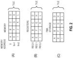
- Portions of storage are arranged into tiles of different horizontal and vertical dimensions.
- a tile may have horizontal dimension of 4 (e.g., four rows of a matrix) and a vertical dimension of 8 (e.g., 8 columns of the matrix).
- the horizontal dimension is related to element sizes (e.g., 2-, 4-, 8-, 16-, 32-, 64-, 128-bit, etc.).
- Multiple datatypes single precision floating-point, double precision floating-point, integer, etc. may be supported.
- tile parameters can be configured.
- a given tile may be configured to provide tile options.
- Exemplary tile options include but are not limited to: a number of rows of the tile, a number of columns of the tile, whether the tile is VALID, and/or whether the tile consists of a PAIR of equal-sized tiles.
- this configuration is consistent with a palette, used to provide tile options, supplying at least 4 names with total storage of at least 4 kB.
- the tiles can be loaded from and stored to memory using load and store operations.
- the amount of available application memory, as well as the size, number, and configuration of available tiles varies.
- Tile t5L 128 and tile t5R 130 have K rows and N/2 columns of 8-byte elements (e.g., double precision floating-point data). As the double precision operands are twice the width of single precision, this configuration is consistent with a palette, used to provide tile options, supplying at least 2 names with total storage of at least 4 kB.
- the four tiles of Figure 1A use 4 names, each naming a 1 kB tile, whereas the 2 pairs of tiles in Figure 1B can use 2 names to specify the paired tiles.
- tile instructions accept a name of a paired tile as an operand. In operation, the tiles can be loaded from and stored to memory using load and store operations. Depending upon the instruction encoding scheme used, the amount of available application memory, as well as the size, number, and configuration of available tiles varies.
- tile parameters are definable.
- a "palette" is used to provide tile options.
- Exemplary options include, but are not limited to: the number of tile names, the number of bytes in a row of storage, the number of rows and columns in a tile, etc.
- an application can be written such that a fixed usage of names will be able to take advantage of different storage sizes across implementations.
- Tile loads from memory and stores to memory are typically strided accesses from the application memory to packed rows of data.
- Exemplary TILELOAD and TILES TORE instructions, or other instruction references to application memory as a TILE operand in load-op instructions are, in some embodiments, restartable to handle (up to) 2*rows of page faults, unmasked floating-point exceptions, and/or interrupts per instruction.
- the supported parameters for the TMMA architecture are reported via CPUID.
- the list of information includes a maximum height and a maximum S ⁇ VID dimension.
- Configuring the TMMA architecture requires specifying the dimensions for each tile, the element size for each tile and the palette identifier. This configuration is done by executing the TILECONFIG instruction.
- Exiting a tile region is typically done with the TILERELEASEALL instruction. It takes no parameters and swiftly invalidates all tiles (indicating that the data no longer needs any saving or restoring) and clears the internal state corresponding to being in a tile region.
- Context save (e.g., XSAVE) exposes the entire TILE storage area when writing it to memory. If XRSTOR loaded garbage data into the rightmost part of a tile, that data will be saved by XSAVE. XSAVE will write zeros for rows beyond the number specified for each tile.
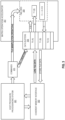
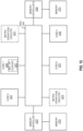
- FIG. 3 illustrates an embodiment of a system utilizing a matrix (tile) operations accelerator.
- a host processor/processing system 301 communicates commands 311 (e.g., matrix manipulation operations such as arithmetic or matrix manipulation operations, or load and store operations) to a matrix operations accelerator 307.
- commands 311 e.g., matrix manipulation operations such as arithmetic or matrix manipulation operations, or load and store operations
- this accelerator 307 may be a part of a processing core.
- commands 311 that are tile manipulation operator instructions will refer to tiles as register-register (“reg-reg") or register-memory (“reg-mem”) format.
- Other commands such as TILESTORE, TILELOAD, TILECONFIG, etc., do not perform data operations on a tile.
- Commands may be decoded instructions (e.g., micro-ops) or macro-instructions for the accelerator 307 to handle.
- a coherent memory interface 303 is coupled to the host processor/processing system 301 and matrix operations accelerator 307 such that they can share memory.
- Figures 4 and 5 show different embodiments of how memory is shared using a matrix operations accelerator.
- the host processor 401 and matrix operations accelerator circuitry 405 share the same memory 403.
- Figure 5 illustrates an embodiment where the host processor 501 and matrix operations accelerator 505 do not share memory but can access each other's memory.
- processor 501 can access tile memory 507 and utilize its host memory 503 as normal.
- the matrix operations accelerator 505 can access host memory 503, but more typically uses its own memory 507. Note these memories may be of different types.
- the elements of matrix B are spread across the rectangular grid of FMAs.
- Matrix B (stored in tile A 601) has its elements of a row transformed to match up with the columnar dimension of the rectangular grid of FMAs.
- an element of A and B are multiplied and added to the incoming summand (from above in the Figure) and the outgoing sum is passed to the next row of FMAs (or the final output).
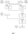
- Figure 7 illustrates an embodiment of a subset of the execution of an iteration of a chained fused multiply accumulate instruction.
- this illustrates execution circuitry of an iteration of one packed data element position of the destination.
- the chained fused multiply accumulate is operating on signed sources wherein the accumulator is 2x the input data size.
- the result of the addition of the results of the multiplications is added to the data from most significant packed data element position of the signed source 3 709 (using a different adder 713 or the same adder 711).
- a first signed source (source 1 801) and a second signed source (source 2 803) each have four packed data elements. Each of these packed data elements stores signed data such as integer data.
- a third signed source (source 3 809) has two packed data elements, each of which stores signed data.
- the sizes of the first and second signed sources 801 and 803 are half that of the third signed source 809.
- the first and second signed sources 801 and 803 could have 32-bit packed data elements (e.g., single precision floating-point)
- the third signed source 809 could have 64-bit packed data elements (e.g., double precision floating-point).
- packed data elements are processed in pairs. For example, the data of the most significant packed data element positions of the first and second signed sources 801 and 803 are multiplied using a multiplier circuit 805, and the data from second most significant packed data element positions of the first and second signed sources 801 and 803 are multiplied using a multiplier circuit 807.
- multiplier circuits 805 and 807 perform the multiplications with infinite precision without saturation and use adder/saturation circuitry 813 to saturate the results of the accumulation to plus or minus infinity in case of an overflow and to zero in case of any underflow. In other embodiments, multiplier circuits 805 and 807 perform the saturation themselves.
- these multiplier circuits 805 and 807 are reused for other packed data element positions. In other embodiments, additional multiplier circuits are used so that the packed data elements are processed in parallel. In some contexts, parallel execution is done using lanes that are the size of the signed third source (initial value or previous iteration result) 809. The results of each of the multiplications are added to the signed third source 809 using addition/saturation circuitry 813.
- Addition/saturation (accumulator) circuitry 813 preserves a sign of an operand when the addition results in a value that is too big. In particular, saturation evaluation occurs on the infinite precision result between the multi-way-add and the write to the destination or next iteration.
- the accumulator 813 is floating-point and the input terms are integer, the sum of products and the floating-point accumulator input value are turned into infinite precision values (fixed point numbers of hundreds of bits), the addition of the multiplication results and the third input is performed, and a single rounding to the actual accumulator type is performed.
- the result of the addition and saturation check is stored into the signed result 815 in a packed data element position that corresponds to the packed data element position used from the signed third source 809 or passed on to the next iteration if there is one.
- a writemask is applied to this storage such that if a corresponding writemask (bit) is set, the storage happens, and, if not set, the storage does not happen.
- Figure 9 illustrates an embodiment of a subset of the execution of an iteration of a chained fused multiply accumulate instruction.
- this illustrates execution circuitry of an iteration of one packed data element position of the destination.
- the chained fused multiply accumulate is operating on a signed source and an unsigned source wherein the accumulator is 4x the input data size.
- a first signed source (source 1 901) and a second unsigned source (source 2 903) each have four packed data elements. Each of these packed data elements has data such as floating-point or integer data.
- a third signed source (initial value or result 915) has a packed data element of which stores signed data.
- the sizes of the first and second sources 901 and 903 are a quarter of the third signed source 915.
- the first and second sources 901 and 903 could have 16-bit packed data elements (e.g., word) and the third signed source 915 could have 64-bit packed data elements (e.g., double precision floating-point or 64-bit integer).
- packed data elements are processed in quadruplets. For example, the data of the most significant packed data element positions of the first and second sources 901 and 903 are multiplied using a multiplier circuit 905, data from second most significant packed data element positions of the first and second sources 901 and 903 are multiplied using a multiplier circuit 907, data from third most significant packed data element positions of the first and second sources 901 and 903 are multiplied using a multiplier circuit 909, and data from the least significant packed data element positions of the first and second sources 901 and 903 are multiplied using a multiplier circuit 911.
- the signed packed data elements of the first source 901 are sign extended and the unsigned packed data elements of the second source 903 are zero extended prior to the multiplications.
- these multiplier circuits 905-911 are reused for other packed data elements positions. In other embodiments, additional multiplier circuits are used so that the packed data elements are processed in parallel. In some contexts, parallel execution is done using lanes that are the size of the signed third source 915. The results of each of the multiplications are added using addition circuitry 913.
- the result of the addition of the results of the multiplications is added to the data from most significant packed data element position of the signed source 3 915 (using a different adder 917 or the same adder 913).
- the result 919 of the second addition is either stored into the signed destination in a packed data element position that corresponds to the packed data element position used from the signed third source 915 or passed to the next iteration.
- a writemask is applied to this storage such that if a corresponding writemask (bit) is set, the storage happens, and, if not set, the storage does not happen.
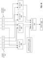
- Figure 10 illustrates an embodiment of a subset of the execution of an iteration of chained fused multiply accumulate instruction.
- this illustrates execution circuitry of an iteration of one packed data element position of the destination.
- the chained fused multiply accumulate is operating on a signed source and an unsigned source wherein the accumulator is 4x the input data size.
- a first signed source 1001 and a second unsigned source 1003 each have four packed data elements. Each of these packed data elements stores data such as floating-point or integer data.
- a third signed source 1015 (initial or previous result) has a packed data element of which stores signed data. The sizes of the first and second sources are a quarter of the third signed source 1015 (initial or previous result).
- the first and second sources could have 16-bit packed data elements (e.g., word) and the third signed source 1015 (initial or previous result) could have 64-bit packed data elements (e.g., double precision floating-point or 64-bit integer).
- packed data elements are processed in quadruplets. For example, the data of the most significant packed data element positions of the first signed source 1001 and the second unsigned source 1003 are multiplied using a multiplier circuit 1005, data from second most significant packed data element positions of the first signed source 1001 and the second unsigned source 1003 are multiplied using a multiplier circuit 1007, data from third most significant packed data element positions of the first signed source 1001 and the second unsigned source 1003 are multiplied using a multiplier circuit 1009, and data from the least significant packed data element positions of the first signed source 1001 and the second unsigned source 1003 are multiplied using a multiplier circuit 1011.
- the signed packed data elements of the first signed source 1001 are sign extended and the unsigned packed data elements of the second unsigned source 1003 are zero extended prior to the multiplications.
- these multiplier circuits 1005-1011 are reused for other packed data elements positions. In other embodiments, additional multiplier circuits are used so that the packed data elements are processed in parallel. In some contexts, parallel execution is done using lanes that are the size of third signed source 1015 (initial or previous result). The result of the addition of the results of the multiplications is added to the data from most significant packed data element position of third signed source 1015 (initial or previous result) using adder/saturation 1013 circuitry.
- Addition/saturation (accumulator) circuitry 1013 preserves a sign of an operand when the addition results in a value that is too big or too small for signed saturation. In particular, saturation evaluation occurs on the infinite precision result between the multi-way-add and the write to the destination.
- the accumulator 1013 is floating-point and the input terms are integer, the sum of products and the floating-point accumulator input value are turned into infinite precision values (fixed point numbers of hundreds of bits), the addition of the multiplication results and the third input is performed, and a single rounding to the actual accumulator type is performed.
- the result 1019 of the addition and saturation check is stored into the signed destination in a packed data element position that corresponds to the packed data element position used from third signed source 1015 (initial or previous result) or passed to the next iteration.
- a writemask is applied to this storage such that if a corresponding writemask (bit) is set, the storage happens, and, if not set, the storage does not happen.
- table 1103 illustrates different configurations.
- the accumulator uses 32-bit integer or single-precision floating-point (SPFP) values that are 32-bit in size.
- SPFP single-precision floating-point
- DPFP double-precision floating-point
- table 1105 illustrates a configuration.
- the accumulator uses 64-bit integer.
- a plurality of cores, core 0 1201, core 1 1203, core 2 1205, and core N 1207 provide non-tile-based instruction support.
- matrix operations circuitry 1251 is provided in a core 1203, and in other embodiments matrix operations circuitry 1211 and 1213 are accessible on the ring interconnect 1245.
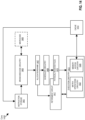
- Figure 13 illustrates an embodiment of a processor core pipeline supporting matrix operations using tiles.
- Branch prediction and decode circuitry 1303 performs branch predicting of instructions, decoding of instructions, and/or both from instructions stored in instruction storage 1301. For example, instructions detailed herein may be stored in instruction storage. In some implementations, separate circuitry is used for branch prediction and in some embodiments, at least some instructions are decoded into one or more micro-operations, microcode entry points, microinstructions, other instructions, or other control signals using microcode 1305.
- the branch prediction and decode circuitry 1303 may be implemented using various different mechanisms. Examples of suitable mechanisms include, but are not limited to, look-up tables, hardware implementations, programmable logic arrays (PLAs), microcode read only memories (ROMs), etc.
- the scheduler circuitry 1309 represents any number of different schedulers, including reservations stations, central instruction window, etc.
- the scheduler circuitry 1309 is coupled to, or includes, physical register file(s) 1315.
- Each of the physical register file(s) 1315 represents one or more physical register files, different ones of which store one or more different data types, such as scalar integer, scalar floating-point, packed integer, packed floating-point, vector integer, vector floating-point, status (e.g., an instruction pointer that is the address of the next instruction to be executed), tiles, etc.
- the physical register file(s) 1315 comprises vector registers circuitry, write mask registers circuitry, and scalar registers circuitry.
- the execution circuitry 1311 is a set of one or more execution circuits, including scalar circuitry 1321, vector/SIMD circuitry 1323, and matrix operations circuitry 1327, as well as memory access circuitry 1325 to access cache 1313.
- the execution circuits perform various operations (e.g., shifts, addition, subtraction, multiplication) and on various types of data (e.g., scalar floating-point, packed integer, packed floating-point, vector integer, vector floating-point). While some embodiments may include a number of execution units dedicated to specific functions or sets of functions, other embodiments may include only one execution unit or multiple execution units that all perform all functions.
- the scalar circuitry 1321 performs scalar operations
- the vector/SIMD circuitry 1323 performs vector/SIMD operations
- matrix operations circuitry 1327 performs matrix (tile) operations detailed herein.
- the exemplary register renaming, out-of-order issue/execution core architecture may implement a pipeline as follows: 1) an instruction fetch circuit performs fetch and length decoding stages; 2) the branch and decode circuitry 1303 performs a decode stage; 3) the allocate/rename 1307 circuitry performs an allocation stage and renaming stage; 4) the scheduler circuitry 1309 performs a schedule stage; 5) physical register file(s) (coupled to, or included in, the scheduler circuitry 1309 and allocate/rename 1307 circuitry and a memory unit perform a register read/memory read stage; the execution circuitry 1311 performs an execute stage; 6) a memory unit and the physical register file(s) unit(s) perform a write back/memory write stage; 7) various units may be involved in the exception handling stage; and 8) a retirement unit and the physical register file(s) unit(s) perform a commit stage.
- the core may support multithreading (executing two or more parallel sets of operations or threads), and may do so in a variety of ways including time sliced multithreading, simultaneous multithreading (where a single physical core provides a logical core for each of the threads that physical core is simultaneously multithreading), or a combination thereof (e.g., time sliced fetching and decoding and simultaneous multithreading thereafter such as in the Intel ® Hyperthreading technology).
- Figure 14 illustrates an embodiment of a processor core pipeline supporting matrix operations using tiles.
- Branch prediction and decode circuitry 1403 performs branch predicting of instructions, decoding of instructions, and/or both from instructions stored in instruction storage 1401. For example, instructions detailed herein may be stored in instruction storage. In some implementations, separate circuitry is used for branch prediction and in some embodiments, at least some instructions are decoded into one or more micro-operations, microcode entry points, microinstructions, other instructions, or other control signals using microcode 1405.
- the branch prediction and decode circuitry 1403 may be implemented using various different mechanisms. Examples of suitable mechanisms include, but are not limited to, look-up tables, hardware implementations, programmable logic arrays (PLAs), microcode read only memories (ROMs), etc.
- the core may support one or more instructions sets (e.g., the x86 instruction set (with some extensions that have been added with newer versions); the MIPS instruction set of MIPS Technologies of Sunnyvale, CA; the ARM instruction set (with optional additional extensions such as NEON) of ARM Holdings of Sunnyvale, CA), including the instruction(s) described herein.
- the core 1490 includes logic to support a packed data instruction set extension (e.g., AVX1, AVX2), thereby allowing the operations used by many multimedia applications to be performed using packed data.
- the core may support multithreading (executing two or more parallel sets of operations or threads), and may do so in a variety of ways including time sliced multithreading, simultaneous multithreading (where a single physical core provides a logical core for each of the threads that physical core is simultaneously multithreading), or a combination thereof (e.g., time sliced fetching and decoding and simultaneous multithreading thereafter such as in the Intel ® Hyperthreading technology).
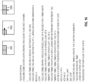
- Figure 15 illustrates an example of a matrix expressed in row major format and column major format.
- matrix A is a 2x3 matrix.
- the data elements of a row are consecutive.
- the data elements of a column are consecutive.
- the input matrices would be stored in linear memory (column-major) as:
- the transform matrix is out and can then be stored in in row-major order: ag+bh cg+dh eg+fh ai+bj ci+dj ei+fj ak+bl ck+dl ek+fl and used in subsequent column major computations, it is the correct un-transformed matrix: ag+bh ai+bj ak+bl cg+dh ci+dj ck+dl eg+fh ei+fj ek+fl
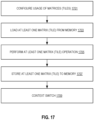
- Figure 17 illustrates an embodiment of usage of matrices (e.g., tiles).
- tile usage is configured.
- a TILECONFIG instruction is executed to configure tile usage including setting a number of rows and columns per tile.
- at least one matrix (tile) is loaded from memory at 1703.
- At least one matrix (tile) operation is performed at 1705 using the matrices (e.g., tiles).
- at least one matrix (tile) is stored out to memory and a context switch can occur at 1709.
- Instruction execution resources 1811 of a processor/core 1805 stores aspects of a tile description 1803 into tile configurations 1817.
- the tile configurations 1817 include palette table 1813 to detail what tiles for a palette are configured (the number of rows and columns in each tile) and a marking that matrix support is in use.
- instruction execution resources 1811 are configured to use tiles as specified by the tile configurations 1817.
- the instruction execution resources 1811 may also include a machine specific register or configuration register to indicate tile usage. Additional values such as in-use and start values are also set.
- the tile configurations 1817 utilize register(s) 1819 to store tile usage and configuration information.
- Figure 19 illustrates an embodiment of a description of the matrices (e.g., tiles) to be supported. This is the description that is to be stored upon an execution of a STTILECFG instruction.
- each field is a byte.
- a palette ID 1901 is stored. The palette ID is used to index a palette table 1813 which stores, per palette ID, a number of bytes in a tile, and bytes per row of the tiles that are associated with this ID as defined by the configuration.
- Byte 1 stores a value to be stored in a "startRow" register 1903 and byte 2 stores a value to be stored in a register, startP 1905.
- the instructions store information these registers.
- the instructions store information in these registers.
- the startRow value indicates the row that should be used for restart.
- the startP value indicates the position within the row for store operations when pairs are used and, in some embodiments, indicates the lower half of the row (in the lower tile of a pair) or higher half of the row (in the higher tile of a pair). Generally, the position in the row (the column) is not needed.
- Bytes 16-17 store the number of rows 1913 and columns 1915 for tile 0
- bytes 18-19 store the number of rows and columns for tile 1, etc.
- each 2-byte group specifies a number of rows and columns for a tile. If a group of 2 bytes is not used to specify tile parameters, they should have the value zero. Specifying tile parameters for more tiles than the implementation limit or the palette limit results in a fault. Unconfigured tiles are set to an initial state with 0 rows, 0 columns.
- the configuration in memory typically ends with an ending delineation such as all zeros for several consecutive bytes.
- Figures 20(A) -(D) illustrate examples of register(s) 1819.
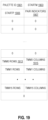
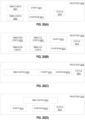
- Figure 20(A) illustrates a plurality of registers 1819. As shown each tile (TMM0 2001 ... TMMN 2003) has a separate register with each register storing a row and column size for that particular tile. StartP 2011 and StartRow 2013 are stored in separate registers.
- Figure 20(B) illustrates a plurality of registers 1819. As shown each tile has separate registers for its rows and columns. For example, TMM0 rows configuration 2021, TMM0 columns configuration 2023, StartP 2011 and StartRow 2013 are stored in separate registers.
- the processor will also include other supporting hardware, such as decode circuitry to decode the fetched instruction, and execution circuitry to respond to the decoded instruction as specified by the opcode, e.g., execution circuitry that causes a matrix operations accelerator (e.g., matrix operations accelerator 307 in Figure 3 ) to perform one or more (e.g., all) of the actions of the TDPBF8PS instruction.
- decode circuitry to decode the fetched instruction
- execution circuitry to respond to the decoded instruction as specified by the opcode
- execution circuitry e.g., execution circuitry that causes a matrix operations accelerator (e.g., matrix operations accelerator 307 in Figure 3 ) to perform one or more (e.g., all) of the actions of the TDPBF8PS instruction.
- a matrix operations accelerator e.g., matrix operations accelerator 307 in Figure 3
- processor 2100 (for example, matrix operations circuitry, e.g., as part of a matrix operations accelerator) is then to use multiply circuit 2118 to multiply the K pairs of converted first quad values from the two specified source matrices (e.g., tiles) to generate K first products, multiply the K pairs of converted second quad values from the specified source matrices (e.g., tiles) to generate K second products, multiply the K pairs of converted third quad values from the specified source matrices (e.g., tiles) to generate K third products, and multiple the K pairs of converted fourth quad values from the specified source matrices (e.g., tiles) to generate K fourth products, and then use accumulate circuit 2120 to accumulate those products separately, including a first sum of the K first products, a second sum of the K second products, a third sum of the K third products, and a fourth sum of the K fourth products, accumulate the first, second, third, and fourth sums with previous contents of the element (M,N), e.g., shown in the example
- Figure 22B is pseudocode 2220 for exemplary helper functions for use with a TDPBF8PS instruction, according to some embodiments.
- pseudocode 2220 defines a convert_bf8_to_fp32() function, a write_row_and _zero() function, a zero_upper_rows() function, and a zero_tileconfig_start() function, all of which may be used by TDPBF8PS pseudocode of Figure 22A .
- TDPBF8PS instruction Execution of a TDPBF8PS instruction is further illustrated and described with respect to Figures 21 , 22A-B , 23 , 28A-B , and 29A-B .
- Example formats of TDPBF8PS instructions is further illustrated and described with respect to Figures 24-26D .
- Example execution circuitry is further illustrated and described with respect to Figures 3- 14.
- execution circuitry caused execution by (e.g., offload to) a matrix operations accelerator, such as that illustrated and described as accelerator 307 ( Figure 3 ).
- execution circuitry is a matrix operations circuit, such as matrix operations circuitry 405 ( Figure 4 ), 505 ( Figure 5 ), or 1213 ( Figure 12 ), and 1327 ( Figure 13 ).
- one or more of optional instructions modifiers 2410, 2412, 2414, and 2416 are encoded in an immediate field (not shown) optionally included with the instruction 2400. In some embodiments, one or more of optional instructions modifiers 2410, 2412, 2414, and 2416 are specified via a configuration/status register (e.g., XTILECONFIG).
- a configuration/status register e.g., XTILECONFIG
- a 64 byte vector operand length (or size) with 32 bit (4 byte) or 64 bit (8 byte) data element widths (or sizes) (and thus, a 64 byte vector consists of either 16 doubleword-size elements or alternatively, 8 quadword-size elements); a 64 byte vector operand length (or size) with 16 bit (2 byte) or 8 bit (1 byte) data element widths (or sizes); a 32 byte vector operand length (or size) with 32 bit (4 byte), 64 bit (8 byte), 16 bit (2 byte), or 8 bit (1 byte) data element widths (or sizes); and a 16 byte vector operand length (or size) with 32 bit (4 byte), 64 bit (8 byte), 16 bit (2 byte), or 8 bit (1 byte) data element widths (or sizes); alternative embodiments may support more, less and/or different vector operand sizes (e.g., 256 byte vector operands) with more, less, or different data element widths
- Write mask field 2570 its content controls, on a per data element position basis, whether that data element position in the destination vector operand reflects the result of the base operation and augmentation operation.
- Class A instruction templates support merging-writemasking
- class B instruction templates support both merging- and zeroing-writemasking.
- one of the graphics cores intended primarily for graphics and/or scientific computing may support only class A, while one or more of the general-purpose cores may be high-performance general-purpose cores with out of order execution and register renaming intended for general-purpose computing that support only class B.
- Another processor that does not have a separate graphics core may include one more general purpose in-order or out-of-order cores that support both class A and class B.
- features from one class may also be implement in the other class in different embodiments.
- Programs written in a high level language would be put (e.g., just in time compiled or statically compiled) into an variety of different executable forms, including: 1) a form having only instructions of the class(es) supported by the target processor for execution; or 2) a form having alternative routines written using different combinations of the instructions of all classes and having control flow code that selects the routines to execute based on the instructions supported by the processor which is currently executing the code.
- the generic vector friendly instruction format 2500 includes the following fields listed below in the order illustrated in Figure 26A .
- EVEX Prefix 2602 (Bytes 0-3)- is encoded in a four-byte form.
- Rrrr, xxx, and bbb may be formed by adding EVEX.R, EVEX.X, and EVEX.B.
- REX' field 2510 - this is the first part of the REX' field 2510 and is the EVEX.R' bit field (EVEX Byte 1, bit [4] - R') that is used to encode either the upper 16 or lower 16 of the extended 32 register set.
- this bit along with others as indicated below, is stored in bit inverted format to distinguish (in the well-known x86 32-bit mode) from the BOUND instruction, whose real opcode byte is 62, but does not accept in the MOD R/M field (described below) the value of 11 in the MOD field; alternative embodiments do not store this and the other indicated bits below in the inverted format.
- a value of 1 is used to encode the lower 16 registers.
- R'Rrrr is formed by combining EVEX.R', EVEX.R, and the other RRR from other fields.
- EVEX.vvw 2620 (EVEX Byte 2, bits [6:3]-vvvv)- the role of EVEX.vvw may include the following: 1) EVEX.vvw encodes the first source register operand, specified in inverted (1s complement) form and is valid for instructions with 2 or more source operands; 2) EVEX.vvw encodes the destination register operand, specified in 1s complement form for certain vector shifts; or 3) EVEX.vwv does not encode any operand, the field is reserved and should contain 111 1b.
- EVEX.vvvv field 2620 encodes the 4 low-order bits of the first source register specifier stored in inverted (1s complement) form. Depending on the instruction, an extra different EVEX bit field is used to extend the specifier size to 32 registers.
- Write mask field 2570 (EVEX byte 3, bits [2:0]-kkk) - its content specifies the index of a register in the write mask registers as previously described.
- SIB Scale, Index, Base
- Displacement field 2562A (Bytes 7-10) - when MOD field 2642 contains 10, bytes 7-10 are the displacement field 2562A, and it works the same as the legacy 32-bit displacement (disp32) and works at byte granularity.
- the displacement factor field 2562B is encoded the same way as an x86 instruction set 8-bit displacement (so no changes in the ModRM/SIB encoding rules) with the only exception that disp8 is overloaded to disp8*N. In other words, there are no changes in the encoding rules or encoding lengths but only in the interpretation of the displacement value by hardware (which needs to scale the displacement by the size of the memory operand to obtain a byte-wise address offset).
- Immediate field 2572 operates as previously described.
- Figure 26B is a block diagram illustrating the fields of the specific vector friendly instruction format 2600 that make up the full opcode field 2574 according to one embodiment.
- the full opcode field 2574 includes the format field 2540, the base operation field 2542, and the data element width (W) field 2564.
- the base operation field 2542 includes the prefix encoding field 2625, the opcode map field 2615, and the real opcode field 2630.
- Figure 26C is a block diagram illustrating the fields of the specific vector friendly instruction format 2600 that make up the register index field 2544 according to one embodiment.
- the register index field 2544 includes the REX 2605 field, the REX' 2610 field, the MODR/M.reg field 2644, the MODR/M.r/m field 2646, the VVVV field 2620, xxx field 2654, and the bbb field 2656.
- the vector length field 2559B selects between a maximum length and one or more other shorter lengths, where each such shorter length is half the length of the preceding length; and instructions templates without the vector length field 2559B operate on the maximum vector length.
- the class B instruction templates of the specific vector friendly instruction format 2600 operate on packed or scalar single/double-precision floating-point data and packed or scalar integer data. Scalar operations are operations performed on the lowest order data element position in a zmm/ymm/xmm register; the higher order data element positions are either left the same as they were prior to the instruction or zeroed depending on the embodiment.
- Scalar floating-point stack register file (x87 stack) 2745 on which is aliased the MMX packed integer flat register file 2750 - in the embodiment illustrated, the x87 stack is an eight-element stack used to perform scalar floating-point operations on 32/64/80-bit floating-point data using the x87 instruction set extension; while the MMX registers are used to perform operations on 64-bit packed integer data, as well as to hold operands for some operations performed between the MMX and XMM registers.
- the core 2890 includes a microcode ROM or other medium that stores microcode for certain macroinstructions (e.g., in decode unit 2840 or otherwise within the front-end unit 2830).
- the decode unit 2840 is coupled to a rename/allocator unit 2852 in the execution engine unit 2850.
- the exemplary register renaming, out-of-order issue/execution core architecture may implement the pipeline 2800 as follows: 1) the instruction fetch 2838 performs the fetch and length decoding stages 2802 and 2804; 2) the decode unit 2840 performs the decode stage 2806; 3) the rename/allocator unit 2852 performs the allocation stage 2808 and renaming stage 2810; 4) the scheduler unit(s) 2856 performs the schedule stage 2812; 5) the physical register file(s) unit(s) 2858 and the memory unit 2870 perform the register read/memory read stage 2814; the execution cluster 2860 perform the execute stage 2816; 6) the memory unit 2870 and the physical register file(s) unit(s) 2858 perform the write back/memory write stage 2818; 7) various units may be involved in the exception handling stage 2822; and 8) the retirement unit 2854 and the physical register file(s) unit(s) 2858 perform the commit stage 2824.
- Figure 29A is a block diagram of a single processor core, along with its connection to the on-die interconnect network 2902 and with its local subset of the Level 2 (L2) cache 2904, according to embodiments.
- an instruction decoder 2900 supports the x86 instruction set with a packed data instruction set extension.
- An L1 cache 2906 allows low-latency accesses to cache memory into the scalar and vector units.
- different implementations of the processor 3000 may include: 1) a CPU with the special purpose logic 3008 being integrated graphics and/or scientific (throughput) logic (which may include one or more cores), and the cores 3002A-N being one or more general purpose cores (e.g., general purpose in-order cores, general purpose out-of-order cores, a combination of the two); 2) a coprocessor with the cores 3002A-N being a large number of special purpose cores intended primarily for graphics and/or scientific (throughput); and 3) a coprocessor with the cores 3002A-N being a large number of general purpose in-order cores.
- the special purpose logic 3008 being integrated graphics and/or scientific (throughput) logic
- the cores 3002A-N being one or more general purpose cores (e.g., general purpose in-order cores, general purpose out-of-order cores, a combination of the two)
- a coprocessor with the cores 3002A-N being a large number of special purpose
- the cores 3002A-N may be homogenous or heterogeneous in terms of architecture instruction set; that is, two or more of the cores 3002A-N may be capable of execution the same instruction set, while others may be capable of executing only a subset of that instruction set or a different instruction set.
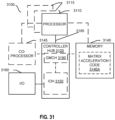
- the memory 3140 may be, for example, dynamic random-access memory (DRAM), phase change memory (PCM), or a combination of the two.
- the controller hub 3120 communicates with the processor(s) 3110, 3115 via a multi-drop bus, such as a frontside bus (FSB), point-to-point interface such as QuickPath Interconnect (QPI), or similar connection 3195.
- a multi-drop bus such as a frontside bus (FSB), point-to-point interface such as QuickPath Interconnect (QPI), or similar connection 3195.
- the coprocessor 3145 is a special-purpose processor, such as, for example, a high-throughput MIC processor, a network or communication processor, compression engine, graphics processor, GPGPU, embedded processor, or the like.
- controller hub 3120 may include an integrated graphics accelerator.
- the processor 3110 executes instructions that control data processing operations of a general type. Embedded within the instructions may be coprocessor instructions. The processor 3110 recognizes these coprocessor instructions as being of a type that should be executed by the attached coprocessor 3145. Accordingly, the processor 3110 issues these coprocessor instructions (or control signals representing coprocessor instructions) on a coprocessor bus or other interconnect, to coprocessor 3145. Coprocessor(s) 3145 accept and execute the received coprocessor instructions.
- multiprocessor system 3200 is a point-to-point interconnect system, and includes a first processor 3270 and a second processor 3280 coupled via a point-to-point interconnect 3250.
- processors 3270 and 3280 may be some version of the processor 3000.
- processors 3270 and 3280 are respectively processors 3110 and 3115, while coprocessor 3238 is coprocessor 3145.
- processors 3270 and 3280 are respectively processor 3110 coprocessor 3145.
- Processors 3270 and 3280 are shown including integrated memory controller (IMC) units 3272 and 3282, respectively.
- Processor 3270 also includes as part of its bus controller units point-to-point (P-P) interfaces 3276 and 3278; similarly, second processor 3280 includes P-P interfaces 3286 and 3288.
- Processors 3270, 3280 may exchange information via a point-to-point (P-P) interface 3250 using P-P interface circuits 3278, 3288.
- IMCs 3272 and 3282 couple the processors to respective memories, namely a memory 3232 and a memory 3234, which may be portions of main memory locally attached to the respective processors.
- Processors 3270, 3280 may each exchange information with a chipset 3290 via individual P-P interfaces 3252, 3254 using point to point interface circuits 3276, 3294, 3286, 3298.
- Chipset 3290 may optionally exchange information with the coprocessor 3238 via a high-performance interface 3292.
- the coprocessor 3238 is a special-purpose processor, such as, for example, a high-throughput MIC processor, a network or communication processor, compression engine, graphics processor, GPGPU, embedded processor, or the like.
- first bus 3216 may be a Peripheral Component Interconnect (PCI) bus, or a bus such as a PCI Express bus or another third generation I/O interconnect bus, although the scope of the present disclosure is not so limited.
- PCI Peripheral Component Interconnect
- Various devices may be coupled to a second bus 3220 including, for example, a keyboard and/or mouse 3222, communication devices 3227 and a storage unit 3228 such as a disk drive or other mass storage device which may include instructions/code and data 3230, in one embodiment.
- a storage unit 3228 such as a disk drive or other mass storage device which may include instructions/code and data 3230, in one embodiment.
- an audio I/O 3224 may be coupled to the second bus 3220.
- a system may implement a multi-drop bus or other such architecture.
- IP cores may be stored on a tangible, machine readable medium and supplied to various customers or manufacturing facilities to load into the fabrication machines that actually make the logic or processor.
Landscapes
- Engineering & Computer Science (AREA)
- Theoretical Computer Science (AREA)
- Software Systems (AREA)
- Physics & Mathematics (AREA)
- General Physics & Mathematics (AREA)
- General Engineering & Computer Science (AREA)
- Mathematical Physics (AREA)
- Mathematical Optimization (AREA)
- Pure & Applied Mathematics (AREA)
- Mathematical Analysis (AREA)
- Computational Mathematics (AREA)
- Computing Systems (AREA)
- Data Mining & Analysis (AREA)
- Life Sciences & Earth Sciences (AREA)
- Biomedical Technology (AREA)
- Health & Medical Sciences (AREA)
- Biophysics (AREA)
- General Health & Medical Sciences (AREA)
- Computational Linguistics (AREA)
- Molecular Biology (AREA)
- Artificial Intelligence (AREA)
- Neurology (AREA)
- Evolutionary Computation (AREA)
- Algebra (AREA)
- Databases & Information Systems (AREA)
- Advance Control (AREA)
- Complex Calculations (AREA)
- Executing Machine-Instructions (AREA)
Applications Claiming Priority (2)
| Application Number | Priority Date | Filing Date | Title |
|---|---|---|---|
| US17/134,373 US12020028B2 (en) | 2020-12-26 | 2020-12-26 | Apparatuses, methods, and systems for 8-bit floating-point matrix dot product instructions |
| EP21196474.7A EP4020169A1 (fr) | 2020-12-26 | 2021-09-14 | Appareils, procédés et systèmes pour des instructions de produit à points de matrice 8 bits à virgule flottante |
Related Parent Applications (1)
| Application Number | Title | Priority Date | Filing Date |
|---|---|---|---|
| EP21196474.7A Division EP4020169A1 (fr) | 2020-12-26 | 2021-09-14 | Appareils, procédés et systèmes pour des instructions de produit à points de matrice 8 bits à virgule flottante |
Publications (2)
| Publication Number | Publication Date |
|---|---|
| EP4398097A2 true EP4398097A2 (fr) | 2024-07-10 |
| EP4398097A3 EP4398097A3 (fr) | 2024-09-04 |
Family
ID=77774690
Family Applications (3)
| Application Number | Title | Priority Date | Filing Date |
|---|---|---|---|
| EP21196474.7A Pending EP4020169A1 (fr) | 2020-12-26 | 2021-09-14 | Appareils, procédés et systèmes pour des instructions de produit à points de matrice 8 bits à virgule flottante |
| EP24177816.6A Pending EP4398097A3 (fr) | 2020-12-26 | 2021-09-14 | Appareils, procédés et systèmes pour instructions de produit de point matriciel à virgule flottante à 8 bits |
| EP23195872.9A Pending EP4276608A3 (fr) | 2020-12-26 | 2021-09-14 | Appareils, procédés et systèmes pour des instructions de produit à points de matrice 8 bits à virgule flottante |
Family Applications Before (1)
| Application Number | Title | Priority Date | Filing Date |
|---|---|---|---|
| EP21196474.7A Pending EP4020169A1 (fr) | 2020-12-26 | 2021-09-14 | Appareils, procédés et systèmes pour des instructions de produit à points de matrice 8 bits à virgule flottante |
Family Applications After (1)
| Application Number | Title | Priority Date | Filing Date |
|---|---|---|---|
| EP23195872.9A Pending EP4276608A3 (fr) | 2020-12-26 | 2021-09-14 | Appareils, procédés et systèmes pour des instructions de produit à points de matrice 8 bits à virgule flottante |
Country Status (3)
| Country | Link |
|---|---|
| US (3) | US12020028B2 (fr) |
| EP (3) | EP4020169A1 (fr) |
| CN (3) | CN116880906A (fr) |
Families Citing this family (4)
| Publication number | Priority date | Publication date | Assignee | Title |
|---|---|---|---|---|
| EP4553650A1 (fr) | 2017-03-20 | 2025-05-14 | INTEL Corporation | Systèmes, procédés et appareils de multiplication et d'accumulation de matrice de mosaïque |
| US12423102B2 (en) | 2020-12-26 | 2025-09-23 | Intel Corporation | Instructions to convert from FP16 to BF8 |
| EP4318228B1 (fr) * | 2022-08-03 | 2025-09-10 | INTEL Corporation | Instructions arithmétiques de source à virgule flottante à 8 bits |
| CN117370722B (zh) * | 2023-10-23 | 2025-12-09 | 鹏城实验室 | 并行计算硬件中矩阵乘法运算的处理方法及相关设备 |
Family Cites Families (33)
| Publication number | Priority date | Publication date | Assignee | Title |
|---|---|---|---|---|
| US7209939B2 (en) * | 2002-07-11 | 2007-04-24 | Sun Microsystems, Inc. | Precision improvement method for the Strassen/Winograd matrix multiplication method |
| US8984043B2 (en) * | 2009-12-23 | 2015-03-17 | Intel Corporation | Multiplying and adding matrices |
| US9600281B2 (en) * | 2010-07-12 | 2017-03-21 | International Business Machines Corporation | Matrix multiplication operations using pair-wise load and splat operations |
| US9146867B2 (en) * | 2011-10-31 | 2015-09-29 | Hewlett-Packard Development Company, L.P. | Methods and apparatus to access memory using runtime characteristics |
| US9110713B2 (en) * | 2012-08-30 | 2015-08-18 | Qualcomm Incorporated | Microarchitecture for floating point fused multiply-add with exponent scaling |
| US9292442B2 (en) * | 2013-04-11 | 2016-03-22 | Qualcomm Incorporated | Methods and apparatus for improving performance of semaphore management sequences across a coherent bus |
| TWI557724B (zh) * | 2013-09-27 | 2016-11-11 | 杜比實驗室特許公司 | 用於將 n 聲道音頻節目編碼之方法、用於恢復 n 聲道音頻節目的 m 個聲道之方法、被配置成將 n 聲道音頻節目編碼之音頻編碼器及被配置成執行 n 聲道音頻節目的恢復之解碼器 |
| US9703531B2 (en) * | 2015-11-12 | 2017-07-11 | Arm Limited | Multiplication of first and second operands using redundant representation |
| US10984838B2 (en) * | 2015-11-17 | 2021-04-20 | Advanced Micro Devices, Inc. | Interconnect architecture for three-dimensional processing systems |
| US9952829B2 (en) * | 2016-02-01 | 2018-04-24 | International Business Machines Corporation | Binary fused multiply-add floating-point calculations |
| US10175944B2 (en) * | 2017-04-12 | 2019-01-08 | Intel Corporation | Mixed-precision floating-point arithmetic circuitry in specialized processing blocks |
| WO2018213636A1 (fr) * | 2017-05-17 | 2018-11-22 | Google Llc | Réalisation d'une multiplication de matrice dans un matériel |
| GB2563878B (en) * | 2017-06-28 | 2019-11-20 | Advanced Risc Mach Ltd | Register-based matrix multiplication |
| US10521225B2 (en) * | 2017-06-29 | 2019-12-31 | Oracle International Corporation | Matrix multiplication at memory bandwidth |
| US10210138B2 (en) * | 2017-07-19 | 2019-02-19 | International Business Machines Corporation | Higher accuracy of non-volatile memory-based vector multiplication |
| US11789729B2 (en) * | 2017-12-29 | 2023-10-17 | Intel Corporation | Systems and methods for computing dot products of nibbles in two tile operands |
| US10691413B2 (en) * | 2018-05-04 | 2020-06-23 | Microsoft Technology Licensing, Llc | Block floating point computations using reduced bit-width vectors |
| US10387122B1 (en) * | 2018-05-04 | 2019-08-20 | Olsen Ip Reserve, Llc | Residue number matrix multiplier |
| US10546044B2 (en) * | 2018-05-15 | 2020-01-28 | Apple Inc. | Low precision convolution operations |
| US11093579B2 (en) * | 2018-09-05 | 2021-08-17 | Intel Corporation | FP16-S7E8 mixed precision for deep learning and other algorithms |
| US10990396B2 (en) * | 2018-09-27 | 2021-04-27 | Intel Corporation | Systems for performing instructions to quickly convert and use tiles as 1D vectors |
| US10853067B2 (en) * | 2018-09-27 | 2020-12-01 | Intel Corporation | Computer processor for higher precision computations using a mixed-precision decomposition of operations |
| US10963256B2 (en) * | 2018-09-28 | 2021-03-30 | Intel Corporation | Systems and methods for performing instructions to transform matrices into row-interleaved format |
| US11366663B2 (en) * | 2018-11-09 | 2022-06-21 | Intel Corporation | Systems and methods for performing 16-bit floating-point vector dot product instructions |
| US10963246B2 (en) * | 2018-11-09 | 2021-03-30 | Intel Corporation | Systems and methods for performing 16-bit floating-point matrix dot product instructions |
| US11615307B2 (en) * | 2018-12-06 | 2023-03-28 | MIPS Tech, LLC | Neural network data computation using mixed-precision |
| US11269630B2 (en) * | 2019-03-29 | 2022-03-08 | Intel Corporation | Interleaved pipeline of floating-point adders |
| US11016731B2 (en) * | 2019-03-29 | 2021-05-25 | Intel Corporation | Using Fuzzy-Jbit location of floating-point multiply-accumulate results |
| US11556615B2 (en) * | 2019-05-03 | 2023-01-17 | Tesla, Inc. | Data path for scalable matrix node engine with mixed data formats |
| US11169776B2 (en) * | 2019-06-28 | 2021-11-09 | Intel Corporation | Decomposed floating point multiplication |
| US20210064338A1 (en) * | 2019-08-28 | 2021-03-04 | Nvidia Corporation | Processor and system to manipulate floating point and integer values in computations |
| US20200026745A1 (en) | 2019-09-27 | 2020-01-23 | Intel Corporation | Apparatuses, methods, and systems for instructions of a matrix operations accelerator |
| US11941395B2 (en) * | 2020-09-26 | 2024-03-26 | Intel Corporation | Apparatuses, methods, and systems for instructions for 16-bit floating-point matrix dot product instructions |
-
2020
- 2020-12-26 US US17/134,373 patent/US12020028B2/en active Active
-
2021
- 2021-09-14 EP EP21196474.7A patent/EP4020169A1/fr active Pending
- 2021-09-14 EP EP24177816.6A patent/EP4398097A3/fr active Pending
- 2021-09-14 EP EP23195872.9A patent/EP4276608A3/fr active Pending
- 2021-12-08 CN CN202310859375.2A patent/CN116880906A/zh active Pending
- 2021-12-08 CN CN202410736985.8A patent/CN118605946A/zh active Pending
- 2021-12-08 CN CN202111490110.7A patent/CN114691217A/zh active Pending
-
2023
- 2023-05-05 US US18/313,026 patent/US12056489B2/en active Active
-
2024
- 2024-03-28 US US18/619,570 patent/US20240241722A1/en not_active Abandoned
Also Published As
| Publication number | Publication date |
|---|---|
| US20220206801A1 (en) | 2022-06-30 |
| CN114691217A (zh) | 2022-07-01 |
| US12020028B2 (en) | 2024-06-25 |
| EP4276608A2 (fr) | 2023-11-15 |
| US12056489B2 (en) | 2024-08-06 |
| CN116880906A (zh) | 2023-10-13 |
| US20230315450A1 (en) | 2023-10-05 |
| EP4398097A3 (fr) | 2024-09-04 |
| EP4020169A1 (fr) | 2022-06-29 |
| US20240241722A1 (en) | 2024-07-18 |
| CN118605946A (zh) | 2024-09-06 |
| EP4276608A3 (fr) | 2024-01-10 |
Similar Documents
| Publication | Publication Date | Title |
|---|---|---|
| US12307250B2 (en) | Systems and methods for performing 16-bit floating-point matrix dot product instructions | |
| US20220171627A1 (en) | Systems and methods for performing matrix compress and decompress instructions | |
| EP3629158B1 (fr) | Systèmes et procédés d'exécution d'instructions pour transformer des matrices en format à rangée entrelacée | |
| US11900114B2 (en) | Systems and methods to skip inconsequential matrix operations | |
| US10970076B2 (en) | Systems and methods for performing instructions specifying ternary tile logic operations | |
| EP3929736A1 (fr) | Appareils, procédés et systèmes pour les instructions de déplacement de données entre les tuiles d'un accélérateur d'opérations de matrice et des registres vectoriels | |
| US11269630B2 (en) | Interleaved pipeline of floating-point adders | |
| US20200210188A1 (en) | Systems and methods for performing matrix row- and column-wise permute instructions | |
| EP4191405B1 (fr) | Systèmes, appareils et procédés de génération d'un index par ordre de tri et éléments de réordonnancement basés sur l'ordre de tri | |
| US12056489B2 (en) | Apparatuses, methods, and systems for 8-bit floating-point matrix dot product instructions | |
| US11941395B2 (en) | Apparatuses, methods, and systems for instructions for 16-bit floating-point matrix dot product instructions | |
| EP3716050A2 (fr) | Utilisation de localisation fuzzy-jbit des résultats de multiplication-accumulation à virgule flottante | |
| US11886875B2 (en) | Systems and methods for performing nibble-sized operations on matrix elements |
Legal Events
| Date | Code | Title | Description |
|---|---|---|---|
| PUAI | Public reference made under article 153(3) epc to a published international application that has entered the european phase |
Free format text: ORIGINAL CODE: 0009012 |
|
| STAA | Information on the status of an ep patent application or granted ep patent |
Free format text: STATUS: THE APPLICATION HAS BEEN PUBLISHED |
|
| AC | Divisional application: reference to earlier application |
Ref document number: 4020169 Country of ref document: EP Kind code of ref document: P |
|
| AK | Designated contracting states |
Kind code of ref document: A2 Designated state(s): AL AT BE BG CH CY CZ DE DK EE ES FI FR GB GR HR HU IE IS IT LI LT LU LV MC MK MT NL NO PL PT RO RS SE SI SK SM TR |
|
| PUAL | Search report despatched |
Free format text: ORIGINAL CODE: 0009013 |
|
| AK | Designated contracting states |
Kind code of ref document: A3 Designated state(s): AL AT BE BG CH CY CZ DE DK EE ES FI FR GB GR HR HU IE IS IT LI LT LU LV MC MK MT NL NO PL PT RO RS SE SI SK SM TR |
|
| RIC1 | Information provided on ipc code assigned before grant |
Ipc: G06F 9/30 20180101AFI20240730BHEP |
|
| STAA | Information on the status of an ep patent application or granted ep patent |
Free format text: STATUS: REQUEST FOR EXAMINATION WAS MADE |
|
| 17P | Request for examination filed |
Effective date: 20250228 |