EP4400913A1 - Procédé de métrologie de mise au point et dispositif de métrologie associé - Google Patents
Procédé de métrologie de mise au point et dispositif de métrologie associé Download PDFInfo
- Publication number
- EP4400913A1 EP4400913A1 EP23151845.7A EP23151845A EP4400913A1 EP 4400913 A1 EP4400913 A1 EP 4400913A1 EP 23151845 A EP23151845 A EP 23151845A EP 4400913 A1 EP4400913 A1 EP 4400913A1
- Authority
- EP
- European Patent Office
- Prior art keywords
- product
- parameter
- structures
- exposure
- neighbor
- Prior art date
- Legal status (The legal status is an assumption and is not a legal conclusion. Google has not performed a legal analysis and makes no representation as to the accuracy of the status listed.)
- Withdrawn
Links
Images

Classifications
-
- G—PHYSICS
- G03—PHOTOGRAPHY; CINEMATOGRAPHY; ANALOGOUS TECHNIQUES USING WAVES OTHER THAN OPTICAL WAVES; ELECTROGRAPHY; HOLOGRAPHY
- G03F—PHOTOMECHANICAL PRODUCTION OF TEXTURED OR PATTERNED SURFACES, e.g. FOR PRINTING, FOR PROCESSING OF SEMICONDUCTOR DEVICES; MATERIALS THEREFOR; ORIGINALS THEREFOR; APPARATUS SPECIALLY ADAPTED THEREFOR
- G03F7/00—Photomechanical, e.g. photolithographic, production of textured or patterned surfaces, e.g. printing surfaces; Materials therefor, e.g. comprising photoresists; Apparatus specially adapted therefor
- G03F7/70—Microphotolithographic exposure; Apparatus therefor
- G03F7/70483—Information management; Active and passive control; Testing; Wafer monitoring, e.g. pattern monitoring
- G03F7/7055—Exposure light control in all parts of the microlithographic apparatus, e.g. pulse length control or light interruption
- G03F7/70558—Dose control, i.e. achievement of a desired dose
-
- G—PHYSICS
- G03—PHOTOGRAPHY; CINEMATOGRAPHY; ANALOGOUS TECHNIQUES USING WAVES OTHER THAN OPTICAL WAVES; ELECTROGRAPHY; HOLOGRAPHY
- G03F—PHOTOMECHANICAL PRODUCTION OF TEXTURED OR PATTERNED SURFACES, e.g. FOR PRINTING, FOR PROCESSING OF SEMICONDUCTOR DEVICES; MATERIALS THEREFOR; ORIGINALS THEREFOR; APPARATUS SPECIALLY ADAPTED THEREFOR
- G03F7/00—Photomechanical, e.g. photolithographic, production of textured or patterned surfaces, e.g. printing surfaces; Materials therefor, e.g. comprising photoresists; Apparatus specially adapted therefor
- G03F7/70—Microphotolithographic exposure; Apparatus therefor
- G03F7/70483—Information management; Active and passive control; Testing; Wafer monitoring, e.g. pattern monitoring
- G03F7/70605—Workpiece metrology
- G03F7/70616—Monitoring the printed patterns
- G03F7/70625—Dimensions, e.g. line width, critical dimension [CD], profile, sidewall angle or edge roughness
-
- G—PHYSICS
- G03—PHOTOGRAPHY; CINEMATOGRAPHY; ANALOGOUS TECHNIQUES USING WAVES OTHER THAN OPTICAL WAVES; ELECTROGRAPHY; HOLOGRAPHY
- G03F—PHOTOMECHANICAL PRODUCTION OF TEXTURED OR PATTERNED SURFACES, e.g. FOR PRINTING, FOR PROCESSING OF SEMICONDUCTOR DEVICES; MATERIALS THEREFOR; ORIGINALS THEREFOR; APPARATUS SPECIALLY ADAPTED THEREFOR
- G03F7/00—Photomechanical, e.g. photolithographic, production of textured or patterned surfaces, e.g. printing surfaces; Materials therefor, e.g. comprising photoresists; Apparatus specially adapted therefor
- G03F7/70—Microphotolithographic exposure; Apparatus therefor
- G03F7/70483—Information management; Active and passive control; Testing; Wafer monitoring, e.g. pattern monitoring
- G03F7/70605—Workpiece metrology
- G03F7/70616—Monitoring the printed patterns
- G03F7/70641—Focus
-
- G—PHYSICS
- G03—PHOTOGRAPHY; CINEMATOGRAPHY; ANALOGOUS TECHNIQUES USING WAVES OTHER THAN OPTICAL WAVES; ELECTROGRAPHY; HOLOGRAPHY
- G03F—PHOTOMECHANICAL PRODUCTION OF TEXTURED OR PATTERNED SURFACES, e.g. FOR PRINTING, FOR PROCESSING OF SEMICONDUCTOR DEVICES; MATERIALS THEREFOR; ORIGINALS THEREFOR; APPARATUS SPECIALLY ADAPTED THEREFOR
- G03F7/00—Photomechanical, e.g. photolithographic, production of textured or patterned surfaces, e.g. printing surfaces; Materials therefor, e.g. comprising photoresists; Apparatus specially adapted therefor
- G03F7/70—Microphotolithographic exposure; Apparatus therefor
- G03F7/70483—Information management; Active and passive control; Testing; Wafer monitoring, e.g. pattern monitoring
- G03F7/70605—Workpiece metrology
- G03F7/706835—Metrology information management or control
- G03F7/706837—Data analysis, e.g. filtering, weighting, flyer removal, fingerprints or root cause analysis
Definitions
- the present invention relates to a target arrangement for metrology of a lithographic process and to a method to measure a parameter of a lithographic process.
- a lithographic apparatus is a machine that applies a desired pattern onto a substrate, usually onto a target portion of the substrate.
- a lithographic apparatus can be used, for example, in the manufacture of integrated circuits (ICs).
- a patterning device which is alternatively referred to as a mask or a reticle, may be used to generate a circuit pattern to be formed on an individual layer of the IC.
- This pattern can be transferred onto a target portion (e.g., including part of, one, or several dies) on a substrate (e.g., a silicon wafer). Transfer of the pattern is typically via imaging onto a layer of radiation-sensitive material (resist) provided on the substrate.
- resist radiation-sensitive material
- a single substrate will contain a network of adjacent target portions that are successively patterned.
- it is desirable frequently to make measurements of the structures created e.g., for process control and verification.
- Various tools for making such measurements are known, including scanning electron microscopes, which are often used to measure critical dimension (CD), and specialized tools to measure overlay, a measure of the accuracy of alignment of two layers in a device.
- Overlay may be described in terms of the degree of misalignment between the two layers, for example reference to a measured overlay of 1nm may describe a situation where two layers are misaligned by 1nm.
- scatterometers For use in the lithographic field. These devices direct a beam of radiation onto a target and measure one or more properties of the scattered radiation - e.g., intensity at a single angle of reflection as a function of wavelength; intensity at one or more wavelengths as a function of reflected angle; or polarization as a function of reflected angle - to obtain a "spectrum" from which a property of interest of the target can be determined. Determination of the property of interest may be performed by various techniques: e.g., reconstruction of the target by iterative approaches such as rigorous coupled wave analysis or finite element methods; library searches; and principal component analysis.
- the targets used by conventional scatterometers are relatively large, e.g., 40 ⁇ m by 40 ⁇ m, gratings and the measurement beam generates a spot that is smaller than the grating (i.e., the grating is underfilled). This simplifies mathematical reconstruction of the target as it can be regarded as infinite.
- metrology has been proposed in which the grating is made smaller than the measurement spot (i.e., the grating is overfilled).
- Such targets are measured using dark field scatterometry in which the zeroth order of diffraction (corresponding to a specular reflection) is blocked, and only higher orders processed.
- Examples of dark field metrology can be found in international patent applications WO 2009/078708 and WO 2009/106279 which documents are hereby incorporated by reference in their entirety. Further developments of the technique have been described in patent publications US20110027704A , US20110043791A and US20120242970A . Modifications of the apparatus to improve throughput are described in US2010201963A1 and US2011102753A1 . The contents of all these applications are also incorporated herein by reference. Diffraction-based overlay using dark-field detection of the diffraction orders enables overlay measurements on smaller targets. These targets can be smaller than the illumination spot and may be surrounded by product structures on a wafer (wafer and substrate may be used synonymously throughout this disclosure). Targets can comprise multiple gratings which can be measured in one image.
- CD critical dimension
- Asymmetry in a grating structure can be measured effectively using high-speed inspection apparatus such as a scatterometer, working at visible radiation wavelengths.
- Known focus measuring techniques exploit the fact that focus-sensitive asymmetry can be introduced into structures printed in a resist layer by special design of the patterns on a patterning device that defines the target structure. This may be achieved by defining the structures on the reticle with sub-resolution structures which print with a focus dependent sensitivity manifesting as said focus-sensitive asymmetry.
- EUV lithography where printing is performed using radiation of a wavelength less than 20 nm, for example 13.5 nm, the creation of sub-resolution features becomes more difficult.
- resist thickness, and therefore the thickness of target structures is smaller. This weakens the diffraction efficiency, and hence the signal strength, available for focus metrology.
- the invention in a first aspect provides a method of determining at least one exposure parameter describing an exposure setting of a lithographic exposure process in which a plurality of structures were exposed on a product substrate; the method comprising: obtaining product metrology data describing respective product parameter values relating to at least one product parameter of each said plurality of structures; grouping said product metrology data into a plurality of neighbor groups, each neighbor group describing a different arrangement of said structures; obtaining pre-calibrated sensitivity relationship data for each of said plurality of neighbor groups or different combinations thereof, the sensitivity relationship data relating the calibration metrology data, stratified per neighbor group or different combinations thereof, and said at least one exposure parameter; and inferring said at least one exposure parameter from the product metrology data and pre-calibrated sensitivity relationship data.
- FIG. 1 schematically depicts a lithographic apparatus LA.
- the apparatus includes an illumination optical system (illuminator) IL configured to condition a radiation beam B (e.g., UV radiation or DUV radiation), a patterning device support or support structure (e.g., a mask table) MT constructed to support a patterning device (e.g., a mask) MA and connected to a first positioner PM configured to accurately position the patterning device in accordance with certain parameters; a substrate table (e.g., a wafer table) WT constructed to hold a substrate (e.g., a resist coated wafer) W and connected to a second positioner PW configured to accurately position the substrate in accordance with certain parameters; and a projection optical system (e.g., a refractive projection lens system) PS configured to project a pattern imparted to the radiation beam B by patterning device MA onto a target portion C (e.g., including one or more dies) of the substrate W.
- a radiation beam B e.
- the illumination optical system may include various types of optical or non-optical components, such as refractive, reflective, magnetic, electromagnetic, electrostatic or other types of components, or any combination thereof, for directing, shaping, or controlling radiation.
- optical or non-optical components such as refractive, reflective, magnetic, electromagnetic, electrostatic or other types of components, or any combination thereof, for directing, shaping, or controlling radiation.
- the patterning device support holds the patterning device in a manner that depends on the orientation of the patterning device, the design of the lithographic apparatus, and other conditions, such as for example whether or not the patterning device is held in a vacuum environment.
- the patterning device support can use mechanical, vacuum, electrostatic or other clamping techniques to hold the patterning device.
- the patterning device support may be a frame or a table, for example, which may be fixed or movable as required.
- the patterning device support may ensure that the patterning device is at a desired position, for example with respect to the projection system. Any use of the terms "reticle” or “mask” herein may be considered synonymous with the more general term "patterning device.”
- patterning device used herein should be broadly interpreted as referring to any device that can be used to impart a radiation beam with a pattern in its cross-section such as to create a pattern in a target portion of the substrate. It should be noted that the pattern imparted to the radiation beam may not exactly correspond to the desired pattern in the target portion of the substrate, for example if the pattern includes phase-shifting features or so called assist features. Generally, the pattern imparted to the radiation beam will correspond to a particular functional layer in a device being created in the target portion, such as an integrated circuit.
- the patterning device may be transmissive or reflective.
- Examples of patterning devices include masks, programmable mirror arrays, and programmable LCD panels.
- Masks are well known in lithography, and include mask types such as binary, alternating phase-shift, and attenuated phase-shift, as well as various hybrid mask types.
- An example of a programmable mirror array employs a matrix arrangement of small mirrors, each of which can be individually tilted so as to reflect an incoming radiation beam in different directions. The tilted mirrors impart a pattern in a radiation beam, which is reflected by the mirror matrix.
- the apparatus is of a transmissive type (e.g., employing a transmissive mask).
- the apparatus may be of a reflective type (e.g., employing a programmable mirror array of a type as referred to above, or employing a reflective mask).
- the lithographic apparatus may also be of a type wherein at least a portion of the substrate may be covered by a liquid having a relatively high refractive index, e.g., water, so as to fill a space between the projection system and the substrate.
- a liquid having a relatively high refractive index e.g., water
- An immersion liquid may also be applied to other spaces in the lithographic apparatus, for example, between the mask and the projection system. Immersion techniques are well known in the art for increasing the numerical aperture of projection systems.
- immersion as used herein does not mean that a structure, such as a substrate, must be submerged in liquid, but rather only means that liquid is located between the projection system and the substrate during exposure.
- the illuminator IL receives a radiation beam from a radiation source SO.
- the source and the lithographic apparatus may be separate entities, for example when the source is an excimer laser. In such cases, the source is not considered to form part of the lithographic apparatus and the radiation beam is passed from the source SO to the illuminator IL with the aid of a beam delivery system BD including, for example, suitable directing mirrors and/or a beam expander. In other cases the source may be an integral part of the lithographic apparatus, for example when the source is a mercury lamp.
- the source SO and the illuminator IL, together with the beam delivery system BD if required, may be referred to as a radiation system.
- the illuminator IL may include an adjuster AD for adjusting the angular intensity-distribution of the radiation beam.
- an adjuster AD for adjusting the angular intensity-distribution of the radiation beam.
- the illuminator IL may include various other components, such as an integrator IN and a condenser CO.
- the illuminator may be used to condition the radiation beam, to have a desired uniformity and intensity-distribution in its cross section.
- the radiation beam B is incident on the patterning device (e.g., mask) MA, which is held on the patterning device support (e.g., mask table MT), and is patterned by the patterning device. Having traversed the patterning device (e.g., mask) MA, the radiation beam B passes through the projection optical system PS, which focuses the beam onto a target portion C of the substrate W, thereby projecting an image of the pattern on the target portion C.
- the substrate table WT can be moved accurately, e.g., so as to position different target portions C in the path of the radiation beam B.
- first positioner PM and another position sensor can be used to accurately position the patterning device (e.g., mask) MA with respect to the path of the radiation beam B, e.g., after mechanical retrieval from a mask library, or during a scan.
- Patterning device (e.g., mask) MA and substrate W may be aligned using mask alignment marks M1, M2 and substrate alignment marks P1, P2.
- the substrate alignment marks as illustrated occupy dedicated target portions, they may be located in spaces between target portions (these are known as scribe-lane alignment marks).
- the mask alignment marks may be located between the dies.
- Small alignment markers may also be included within dies, in amongst the device features, in which case it is desirable that the markers be as small as possible and not require any different imaging or process conditions than adjacent features. The alignment system, which detects the alignment markers is described further below.
- Lithographic apparatus LA in this example is of a so-called dual stage type which has two substrate tables WTa, WTb and two stations - an exposure station and a measurement station - between which the substrate tables can be exchanged. While one substrate on one substrate table is being exposed at the exposure station, another substrate can be loaded onto the other substrate table at the measurement station and various preparatory steps carried out.
- the preparatory steps may include mapping the surface control of the substrate using a level sensor LS and measuring the position of alignment markers on the substrate using an alignment sensor AS. This enables a substantial increase in the throughput of the apparatus.
- the depicted apparatus can be used in a variety of modes, including for example a step mode or a scan mode.
- lithographic apparatus is well known to those skilled in the art and need not be described further for an understanding of the present invention.
- the lithographic apparatus LA forms part of a lithographic system, referred to as a lithographic cell LC or a lithocell or cluster.
- the lithographic cell LC may also include apparatus to perform pre- and post-exposure processes on a substrate. Conventionally these include spin coaters SC to deposit resist layers, developers DE to develop exposed resist, chill plates CH and bake plates BK.
- spin coaters SC to deposit resist layers
- developers DE to develop exposed resist
- chill plates CH chill plates
- bake plates BK bake plates
- a substrate handler, or robot, RO picks up substrates from input/output ports I/O1, I/O2, moves them between the different process apparatus and delivers then to the loading bay LB of the lithographic apparatus.
- track control unit TCU which is itself controlled by the supervisory control system SCS, which also controls the lithographic apparatus via lithography control unit LACU.
- SCS supervisory control system
- LACU lithography control unit
- a manufacturing facility in which lithocell LC is located also includes metrology system MET which receives some or all of the substrates W that have been processed in the lithocell. Metrology results are provided directly or indirectly to the supervisory control system SCS. If errors are detected, adjustments may be made to exposures of subsequent substrates, especially if the inspection can be done soon and fast enough that other substrates of the same batch are still to be exposed.
- already exposed substrates may be stripped and reworked to improve yield, or discarded, thereby avoiding performing further processing on substrates that are known to be faulty. In a case where only some target portions of a substrate are faulty, further exposures can be performed only on those target portions which are good.
- an inspection apparatus is used to determine the properties of the substrates, and in particular, how the properties of different substrates or different layers of the same substrate vary from layer to layer.
- the inspection apparatus may be integrated into the lithographic apparatus LA or the lithocell LC or may be a stand-alone device. To enable most rapid measurements, it is desirable that the inspection apparatus measure properties in the exposed resist layer immediately after the exposure.
- the latent image in the resist has a very low contrast - there is only a very small difference in refractive index between the parts of the resist which have been exposed to radiation and those which have not - and not all inspection apparatuses have sufficient sensitivity to make useful measurements of the latent image.
- measurements may be taken after the post-exposure bake step (PEB) which is customarily the first step carried out on exposed substrates and increases the contrast between exposed and unexposed parts of the resist.
- PEB post-exposure bake step
- the image in the resist may be referred to as semi-latent. It is also possible to make measurements of the developed resist image - at which point either the exposed or unexposed parts of the resist have been removed - or after a pattern transfer step such as etching. The latter possibility limits the possibilities for rework of faulty substrates but may still provide useful information.
- the proposed method will comprise a method of measuring one or more exposure parameters, where the one or more exposure parameters may comprise focus and/or dose.
- Focus and dose in this context may relate to respectively a focus setting and a dose setting of a lithographic exposure process on which a measured structure was exposed.
- an alternative metrology method for measuring an exposure parameter e.g., focus and/or dose
- an exposure parameter e.g., focus and/or dose
- the methods disclosed herein are not limited to EUV lithography and can be used to measure the focus parameter in DUV lithography or in lithography generally.
- the proposed method comprises obtaining product metrology data describing at least one product parameter of a plurality of structures such as a plurality of contact holes or vias on a wafer, e.g., using a scanning electron microscope (SEM) or any other suitable metrology device.
- SEM scanning electron microscope
- Contact holes will be assumed throughout this disclosure, although any suitable structure may be used.
- the contact holes are grouped into plurality of neighbor groups, each neighbor group describing, for each structure, an arrangement of neighboring or adjacent structures (e.g., contact holes). Adjacent in this context may mean within a set distance. Structures may be considered adjacent if they are within a distance within which optical proximity effects occur.
- the set distance may be defined as being within 10 times the exposure wavelength (wavelength of the exposure radiation), within 7 times the exposure wavelength or within 5 times the exposure wavelength.
- the distances in absolute terms may be smaller than (about) 65nm, smaller than 95nm or smaller than 130nm.
- Pre-calibrated sensitivity relationships for each of said plurality of neighbor groups are used to infer one or more exposure parameters (e.g., focus and/or dose) from the product metrology data.
- exposure parameters e.g., focus and/or dose
- the product metrology data comprises product displacement data describing a respective displacement (e.g., a placement error with respect to a desired position) of the plurality of structures.
- product displacement data describing a respective displacement (e.g., a placement error with respect to a desired position) of the plurality of structures.
- a product parameter described by the product metrology data may include CD (or any other dimensional parameter), any placement parameter, any shape parameter (e.g., ellipticity) or any roughness values (e.g., contact edge roughness CER, line edge roughness LER or line width roughness LWR). These parameters of interest can also be combined.
- the pre-calibrated sensitivity relationships may be calibrated in an initial calibration step based on measurement of a calibration wafer (e.g., a focus-dose matrix or FEM wafer) where contact holes (or other calibration structures) are exposed at multiple different focus and dose settings.
- the calibration wafer can then be measured for contact hole displacement, the resultant calibration metrology data grouped into a neighbor group and a model determined which relates the calibration metrology data to one or more exposure settings.
- a contact hole neighborhood or neighbor group may be determined for each contact hole, the contact hole neighborhood describing the presence and location of adjacent contact holes (e.g., adjacent in either the x direction or y direction and/or in diagonal directions).
- each contact hole neighborhood may describe whether there are contact holes immediately adjacent orthogonally- i.e., immediately above (or immediately north), immediately below (or immediately south), immediately left (or immediately west) or immediately right (or immediately east) on the wafer plane (e.g., in the X/Y plane).
- each neighborhood may describe whether there are contact holes immediately diagonally, e.g., immediately north-west, immediately north-east, immediately south-east or immediately south-west.
- an arrangement of adjacent structures may describe, for each structure, whether each of a plurality of neighborhood regions within a neighborhood area defined around said structure comprises at least one adjacent structure.
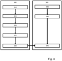
- FIG 3 is a flowchart of a proposed method including a calibration phase 300 and a production phase 305.
- a product parameter such as the contact hole displacement
- the calibration metrology data may comprise calibration x-displacement data relating to displacement in a first direction (or x direction) of the wafer plane and calibration y-displacement data relating to displacement in a second direction (or y direction) of the wafer plane, perpendicular to the first direction.
- the calibration metrology data (relating to all of the measured contact holes or a subset thereof) may be grouped 320 into neighbor groups describing the neighborhood of each contact hole.
- Representative calibration metrology data may be determined from the calibration metrology data (e.g., separately for each of the x-displacement data and y-displacement data).
- This representative calibration metrology data may comprise a representative calibration displacement value in each of the first direction and second direction for each dose-focus setting, per neighbor group.
- the representative calibration value may be an average value for the group; e.g., such as a mean or variance (or a combination of both) of the displacement values within each group.
- this step may yield a mean displacement along the x-direction and y-direction, stratified per neighbor group, for each dose-focus setting used to expose the calibration wafer.
- the variation in displacement with exposure setting is modeled.
- This may comprise, for example, modeling the relationships between the representative calibration metrology data and the set focus/dose values for each neighbor group. For example, this may comprise constructing a matrix of said representative calibration values comprising ( N dose-focus ) ⁇ (2 ⁇ N group ) elements, where N dose-focus is the number of exposure settings or dose-focus settings used to expose the FEM wafer and N group is the number of neighborhood groups (the factor of 2 represents the two displacement directions, x-displacement and y-displacement, assuming two displacement directions are considered separately).
- a suitable model such as a linear regression model or machine learning model may be used to determine 330 sensitivity data comprising the 2 ⁇ N group sensitivities for each neighbor group.
- the number of dose-focus settings used on the calibration or FEM wafer may number more than 50, more than 70, more than 100 or more than 110, for example.
- the modeling may comprise, for each neighbor group, learning the relationships which are able to predict the (known) dose and focus settings using the representative calibration metrology data per group.
- the training may additionally comprise validating the learning e.g., using train-test methods. For example, this may comprise cross-validation on a (e.g., 80%-20%) train-test method.
- a product wafer is exposed 335 and product metrology data (e.g., product displacement data describing displacement of contact holes) measured 340 from a production wafer.
- product metrology data may be grouped into neighbor groups (e.g., per direction).
- the sensitivity data determined at step 330 which describes the relationship between displacement and focus/dose, can be used to infer 345 on-product focus and/or dose based on the product metrology data.
- representative product metrology data may be determined comprising a representative product displacement value (e.g., for each direction) per neighbor group.
- the representative product displacement value may comprise an average (e.g., mean) displacement in each respective direction per neighbor group.
- the representative product displacement value and the respective calibrated relationship for each of the neighbor groups can then be used to infer the focus and/or dose (e.g., per exposure field of the production wafer to determine a focus map and/or dose map describing focus and/or dose over the wafer).
- the inferring step 345 may comprise inferring focus and/or dose from said representative product metrology data and said pre-calibrated sensitivity relationship data relating to each said neighbor group simultaneously, e.g., constructing a matrix of the representative product displacement values comprising 2 ⁇ N group elements and a corresponding number of pre-calibrated sensitivity relationships.
- each field of view (FOV) of the SEM may comprise on the order of thousands of contact holes.
- each FOV may comprise over 2000, over 3000 or over 4000 contact holes. While not all of these contact holes are necessarily grouped and used to determine focus (e.g., not all contact holes necessarily fit into the neighbor groups for which the relationships/sensitivities have been calibrated), it may be that about half or more may be grouped and used in the method disclosed herein.
- the number of FOVs in an exposure field may number more than 10, more than 20 or more than 30 for example. This may result in grouped contact holes per exposure field to number tens of thousands (e.g., more than 50 thousand).
- dedicated targets may be used for the calibration and/or production stages, these dedicated targets being optimized for dose/focus sensitivity and comprising the desired contact hole groups.
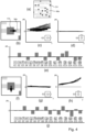
- Figure 4 illustrates schematically some of the steps of the proposed method.
- a product layout ( Figure 4(a) ) comprises for example contact holes CH and metal connections Me. Placement error or displacement in the x direction ( Figure 4(b) ) may be measured for each contact hole.
- the contact holes may be grouped into neighbor groups G1-G16 ( Figure 4(e) ) i.e., according to the neighboring structures. Though these 16 groups are shown, the number of groups and their arrangements may differ from these examples (e.g., not all of these groups need be used).
- Figure 4(e) also shows the representative or mean x-displacement pe x for each of these groups.
- Figures 4(c) and 4(d) comprise sensitivity plots, respectively for neighbor group G2 and G3, of the representative or mean x-displacement pe x with focus f for a plurality of different dose settings (each line comprising a plot for a respective different dose setting). Such plots may be determined for all the other groups.
- Figure 4(d) shows the same number of plots as Figure 4(c) , but the x-displacement for Group G3 is largely invariant to focus and dose variation; this is also apparent from Figure 4(e).
- Figures 4(f) to 4(j) are equivalent respectively to Figures 4(b) to 4(e) , but for y-displacement.
- Each of these sensitivity plots or sensitivity relationships once determined/calibrated, may be used to infer an exposure parameter from similarly grouped metrology data, using the respective corresponding relationship for the metrology data of each group.
- each structure is grouped according to the presence or not of neighbors in each orthogonal direction.
- each neighbor of a structure of interest can be assigned to one of four positions in relation to the structure of interest.
- the groups may be diagonal groups rather than orthogonal groups.
- each neighbor of a structure of interest can be assigned to one of eight positions in relation to the structure of interest and, as such, each structure of interest may be assigned to a respective orthogonal group and a diagonal group.
- sensitivity relationships may be calibrated for each combination of an orthogonal group and a diagonal group.
- the methods above describe a grouping step for grouping the product metrology data into neighbor groups.
- an example classification method is described. This proposed classification method is based on taxonomy which enables identifying similar patterns in logic and is key for dedicated per-class optimization.
- the proposed classification method may comprise for example the following two main stages:
- stage 1 of the proposed method may comprise the following five steps:
- stage 2 of the proposed method may comprise classifying the neighbors according to the outcome of mapping.
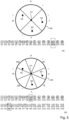
- Figure 5(a) which is similar to the grouping method illustrated in Figure 4 , the neighborhood area NA of a contact hole CH is divided into four quadrants, a "north" quadrant N, a “south” quadrant S, an "east” quadrant E, and a "west” quadrant W.
- the neighborhood defined by neighboring structures N1, N2, N3 can be mapped to a particular group G1-G16 depending on the presence or not of one (or more) neighboring structures N1, N2, N3 in each quadrant.
- the neighborhood area NA of a contact hole CH is divided into eight octants, a "north” octant N, a “south” octant S, an "east” octant E, a “west” octant W, a “northeast” octant NE, a "northwest” octant NW, a “southeast” octant SE and a “southwest” octant SW.
- the eight octants may be divided into two sets: an orthogonal set (N, E, S, W) and a diagonal set (NE, NW, SE, SW).
- the orthogonal set may be assessed for the presence of neighboring structures in the orthogonal octants and mapped accordingly to a corresponding orthogonal group G1-G16.
- the diagonal set may be assessed for the presence of neighboring structures in the diagonal octants and mapped accordingly to a corresponding diagonal group H1-H16.
- the neighborhood of contact hole CH may be described by a combination of orthogonal group and diagonal group, specifically in this example groups G9 and H3.
- the calibrating and using of sensitivity relationship data in the methods disclosed herein may therefore comprise calibrating and using sensitivity relationships for each such combination.
- This taxonomy based classification method may be implemented before the GDS alignment at polygon level. As such, the classification content can be accessible for both metrology and inspection, e.g., by using a SEM or optical-based system.
- the taxonomy based classification method enables contour stacking and discriminated process windows for logic.
- the taxonomy based classification method allows easy interpretation of random logic via data.
- the determined on-product exposure parameter(s) may be fed back in a control loop to control the exposure process; e.g., fed back to the scanner for focus and dose control or corrections.
- inferred focus using the disclosed methods may be used in focus control within the scanner and/or inferred dose using the disclosed methods may be used in dose control (illumination control) within the scanner.
- the inferred focus and/or dose may be used in an optical proximity correction (OPC) control loop.
- OPC optical proximity correction
- imprint lithography a topography in a patterning device defines the pattern created on a substrate.
- the topography of the patterning device may be pressed into a layer of resist supplied to the substrate whereupon the resist is cured by applying electromagnetic radiation, heat, pressure or a combination thereof.
- the patterning device is moved out of the resist leaving a pattern in it after the resist is cured.
- UV radiation e.g., having a wavelength of or about 365, 355, 248, 193, 157 or 126 nm
- EUV radiation e.g., having a wavelength in the range of 5-20 nm
- a well A particle beams such A ion beams or electron beams.
- lens may refer to any one or combination of various types of components, including refractive, reflective, magnetic, electromagnetic and electrostatic components.
Landscapes
- Physics & Mathematics (AREA)
- General Physics & Mathematics (AREA)
- Engineering & Computer Science (AREA)
- Data Mining & Analysis (AREA)
- Exposure And Positioning Against Photoresist Photosensitive Materials (AREA)
Priority Applications (5)
| Application Number | Priority Date | Filing Date | Title |
|---|---|---|---|
| EP23151845.7A EP4400913A1 (fr) | 2023-01-16 | 2023-01-16 | Procédé de métrologie de mise au point et dispositif de métrologie associé |
| KR1020257026455A KR20250137613A (ko) | 2023-01-16 | 2023-12-13 | 포커스 메트롤로지 방법 및 연계된 메트롤로지 디바이스 |
| PCT/EP2023/085669 WO2024153407A1 (fr) | 2023-01-16 | 2023-12-13 | Procédé de métrologie de mise au point et dispositif de métrologie associé |
| CN202380091498.4A CN120476351A (zh) | 2023-01-16 | 2023-12-13 | 焦距量测方法和相关联的量测装置 |
| TW113100548A TW202445260A (zh) | 2023-01-16 | 2024-01-05 | 聚焦度量衡方法及相關度量衡裝置 |
Applications Claiming Priority (1)
| Application Number | Priority Date | Filing Date | Title |
|---|---|---|---|
| EP23151845.7A EP4400913A1 (fr) | 2023-01-16 | 2023-01-16 | Procédé de métrologie de mise au point et dispositif de métrologie associé |
Publications (1)
| Publication Number | Publication Date |
|---|---|
| EP4400913A1 true EP4400913A1 (fr) | 2024-07-17 |
Family
ID=84981465
Family Applications (1)
| Application Number | Title | Priority Date | Filing Date |
|---|---|---|---|
| EP23151845.7A Withdrawn EP4400913A1 (fr) | 2023-01-16 | 2023-01-16 | Procédé de métrologie de mise au point et dispositif de métrologie associé |
Country Status (1)
| Country | Link |
|---|---|
| EP (1) | EP4400913A1 (fr) |
Citations (12)
| Publication number | Priority date | Publication date | Assignee | Title |
|---|---|---|---|---|
| US20060012779A1 (en) * | 2004-07-13 | 2006-01-19 | Asml Netherlands B.V. | Lithographic apparatus and device manufacturing method |
| WO2009078708A1 (fr) | 2007-12-17 | 2009-06-25 | Asml Netherlands B.V. | Outil et procédé de métrologie de superposition à base de diffraction |
| WO2009106279A1 (fr) | 2008-02-29 | 2009-09-03 | Asml Netherlands B.V. | Procédé et appareil de métrologie, appareil lithographique et procédé de fabrication de dispositif |
| US20100201963A1 (en) | 2009-02-11 | 2010-08-12 | Asml Netherlands B.V. | Inspection Apparatus, Lithographic Apparatus, Lithographic Processing Cell and Inspection Method |
| US20110027704A1 (en) | 2009-07-31 | 2011-02-03 | Asml Netherlands B.V. | Methods and Scatterometers, Lithographic Systems, and Lithographic Processing Cells |
| US20110043791A1 (en) | 2009-08-24 | 2011-02-24 | Asml Netherlands B.V. | Metrology Method and Apparatus, Lithographic Apparatus, Device Manufacturing Method and Substrate |
| US20110102753A1 (en) | 2008-04-21 | 2011-05-05 | Asml Netherlands B.V. | Apparatus and Method of Measuring a Property of a Substrate |
| US20120242970A1 (en) | 2010-11-12 | 2012-09-27 | Asml Netherlands B.V. | Metrology Method and Apparatus, and Device Manufacturing Method |
| US20130252176A1 (en) * | 2012-03-22 | 2013-09-26 | Kabushiki Kaisha Toshiba | Method for making correction map of dose amount, exposure method, and method for manufacturing semiconductor device |
| EP3789826A1 (fr) * | 2019-09-05 | 2021-03-10 | ASML Netherlands B.V. | Procédé de détermination de défectuosité de motif basée sur une image post-développement |
| US20220091517A1 (en) * | 2019-01-03 | 2022-03-24 | Asml Netherlands B.V. | Methods and patterning devices and apparatuses for measuring focus performance of a lithographic apparatus, device manufacturing method |
| US20220357672A1 (en) * | 2019-09-26 | 2022-11-10 | Asml Netherlands B.V. | Method for inferring a processing parameter such as focus and associated apparatuses and manufacturing method |
-
2023
- 2023-01-16 EP EP23151845.7A patent/EP4400913A1/fr not_active Withdrawn
Patent Citations (12)
| Publication number | Priority date | Publication date | Assignee | Title |
|---|---|---|---|---|
| US20060012779A1 (en) * | 2004-07-13 | 2006-01-19 | Asml Netherlands B.V. | Lithographic apparatus and device manufacturing method |
| WO2009078708A1 (fr) | 2007-12-17 | 2009-06-25 | Asml Netherlands B.V. | Outil et procédé de métrologie de superposition à base de diffraction |
| WO2009106279A1 (fr) | 2008-02-29 | 2009-09-03 | Asml Netherlands B.V. | Procédé et appareil de métrologie, appareil lithographique et procédé de fabrication de dispositif |
| US20110102753A1 (en) | 2008-04-21 | 2011-05-05 | Asml Netherlands B.V. | Apparatus and Method of Measuring a Property of a Substrate |
| US20100201963A1 (en) | 2009-02-11 | 2010-08-12 | Asml Netherlands B.V. | Inspection Apparatus, Lithographic Apparatus, Lithographic Processing Cell and Inspection Method |
| US20110027704A1 (en) | 2009-07-31 | 2011-02-03 | Asml Netherlands B.V. | Methods and Scatterometers, Lithographic Systems, and Lithographic Processing Cells |
| US20110043791A1 (en) | 2009-08-24 | 2011-02-24 | Asml Netherlands B.V. | Metrology Method and Apparatus, Lithographic Apparatus, Device Manufacturing Method and Substrate |
| US20120242970A1 (en) | 2010-11-12 | 2012-09-27 | Asml Netherlands B.V. | Metrology Method and Apparatus, and Device Manufacturing Method |
| US20130252176A1 (en) * | 2012-03-22 | 2013-09-26 | Kabushiki Kaisha Toshiba | Method for making correction map of dose amount, exposure method, and method for manufacturing semiconductor device |
| US20220091517A1 (en) * | 2019-01-03 | 2022-03-24 | Asml Netherlands B.V. | Methods and patterning devices and apparatuses for measuring focus performance of a lithographic apparatus, device manufacturing method |
| EP3789826A1 (fr) * | 2019-09-05 | 2021-03-10 | ASML Netherlands B.V. | Procédé de détermination de défectuosité de motif basée sur une image post-développement |
| US20220357672A1 (en) * | 2019-09-26 | 2022-11-10 | Asml Netherlands B.V. | Method for inferring a processing parameter such as focus and associated apparatuses and manufacturing method |
Similar Documents
| Publication | Publication Date | Title |
|---|---|---|
| US10417359B2 (en) | Optical metrology of lithographic processes using asymmetric sub-resolution features to enhance measurement | |
| US10725372B2 (en) | Method and apparatus for reticle optimization | |
| IL259564A (en) | Metrological purpose, method and device, computer software and lithographic system | |
| US12007697B2 (en) | Method for process metrology | |
| US12619161B2 (en) | Method for inferring a processing parameter such as focus and associated apparatuses and manufacturing method | |
| TWI796127B (zh) | 一種判定一量測配方之方法及相關度量衡方法與設備 | |
| US12210293B2 (en) | Method for determining a measurement recipe and associated apparatuses | |
| WO2020141040A1 (fr) | Procédés et dispositifs de formation de motifs et appareils pour mesurer les performances de mise au point d'un appareil lithographique, procédé de fabrication de dispositif | |
| CN115210650B (zh) | 用于推断局部均匀性度量的方法 | |
| TW202209018A (zh) | 使用產品特徵上之在解析度度量衡之晶圓對準方法 | |
| US20250021021A1 (en) | Metrology calibration method | |
| EP4474908A1 (fr) | Procédé de métrologie de mise au point et dispositif de métrologie associé | |
| WO2024153407A1 (fr) | Procédé de métrologie de mise au point et dispositif de métrologie associé | |
| US11385554B2 (en) | Metrology apparatus and method for determining a characteristic relating to one or more structures on a substrate | |
| WO2024153591A1 (fr) | Procédé et appareil de détermination de performances de processus de formation de motifs |
Legal Events
| Date | Code | Title | Description |
|---|---|---|---|
| PUAI | Public reference made under article 153(3) epc to a published international application that has entered the european phase |
Free format text: ORIGINAL CODE: 0009012 |
|
| STAA | Information on the status of an ep patent application or granted ep patent |
Free format text: STATUS: THE APPLICATION HAS BEEN PUBLISHED |
|
| AK | Designated contracting states |
Kind code of ref document: A1 Designated state(s): AL AT BE BG CH CY CZ DE DK EE ES FI FR GB GR HR HU IE IS IT LI LT LU LV MC ME MK MT NL NO PL PT RO RS SE SI SK SM TR |
|
| STAA | Information on the status of an ep patent application or granted ep patent |
Free format text: STATUS: THE APPLICATION IS DEEMED TO BE WITHDRAWN |
|
| 18D | Application deemed to be withdrawn |
Effective date: 20250118 |