EP4401144A2 - Integrierte schaltungsanordnung mit einem feldeffekttransistor und verfahren zu deren herstellung - Google Patents
Integrierte schaltungsanordnung mit einem feldeffekttransistor und verfahren zu deren herstellung Download PDFInfo
- Publication number
- EP4401144A2 EP4401144A2 EP23214900.5A EP23214900A EP4401144A2 EP 4401144 A2 EP4401144 A2 EP 4401144A2 EP 23214900 A EP23214900 A EP 23214900A EP 4401144 A2 EP4401144 A2 EP 4401144A2
- Authority
- EP
- European Patent Office
- Prior art keywords
- source
- inventive concept
- horizontal direction
- drain region
- present inventive
- Prior art date
- Legal status (The legal status is an assumption and is not a legal conclusion. Google has not performed a legal analysis and makes no representation as to the accuracy of the status listed.)
- Granted
Links
Images


Classifications
-
- H—ELECTRICITY
- H10—SEMICONDUCTOR DEVICES; ELECTRIC SOLID-STATE DEVICES NOT OTHERWISE PROVIDED FOR
- H10D—INORGANIC ELECTRIC SEMICONDUCTOR DEVICES
- H10D84/00—Integrated devices formed in or on semiconductor substrates that comprise only semiconducting layers, e.g. on Si wafers or on GaAs-on-Si wafers
- H10D84/80—Integrated devices formed in or on semiconductor substrates that comprise only semiconducting layers, e.g. on Si wafers or on GaAs-on-Si wafers characterised by the integration of at least one component covered by groups H10D12/00 or H10D30/00, e.g. integration of IGFETs
- H10D84/82—Integrated devices formed in or on semiconductor substrates that comprise only semiconducting layers, e.g. on Si wafers or on GaAs-on-Si wafers characterised by the integration of at least one component covered by groups H10D12/00 or H10D30/00, e.g. integration of IGFETs of only field-effect components
- H10D84/83—Integrated devices formed in or on semiconductor substrates that comprise only semiconducting layers, e.g. on Si wafers or on GaAs-on-Si wafers characterised by the integration of at least one component covered by groups H10D12/00 or H10D30/00, e.g. integration of IGFETs of only field-effect components of only insulated-gate FETs [IGFET]
- H10D84/834—Integrated devices formed in or on semiconductor substrates that comprise only semiconducting layers, e.g. on Si wafers or on GaAs-on-Si wafers characterised by the integration of at least one component covered by groups H10D12/00 or H10D30/00, e.g. integration of IGFETs of only field-effect components of only insulated-gate FETs [IGFET] comprising FinFETs
-
- H—ELECTRICITY
- H10—SEMICONDUCTOR DEVICES; ELECTRIC SOLID-STATE DEVICES NOT OTHERWISE PROVIDED FOR
- H10D—INORGANIC ELECTRIC SEMICONDUCTOR DEVICES
- H10D64/00—Electrodes of devices having potential barriers
- H10D64/01—Manufacture or treatment
- H10D64/017—Manufacture or treatment using dummy gates in processes wherein at least parts of the final gates are self-aligned to the dummy gates, i.e. replacement gate processes
-
- H—ELECTRICITY
- H10—SEMICONDUCTOR DEVICES; ELECTRIC SOLID-STATE DEVICES NOT OTHERWISE PROVIDED FOR
- H10D—INORGANIC ELECTRIC SEMICONDUCTOR DEVICES
- H10D30/00—Field-effect transistors [FET]
- H10D30/01—Manufacture or treatment
- H10D30/014—Manufacture or treatment of FETs having zero-dimensional [0D] or one-dimensional [1D] channels, e.g. quantum wire FETs, single-electron transistors [SET] or Coulomb blockade transistors
-
- H—ELECTRICITY
- H10—SEMICONDUCTOR DEVICES; ELECTRIC SOLID-STATE DEVICES NOT OTHERWISE PROVIDED FOR
- H10D—INORGANIC ELECTRIC SEMICONDUCTOR DEVICES
- H10D30/00—Field-effect transistors [FET]
- H10D30/01—Manufacture or treatment
- H10D30/019—Manufacture or treatment of FETs having stacked nanowire, nanosheet or nanoribbon channels
- H10D30/0198—Manufacture or treatment of FETs having stacked nanowire, nanosheet or nanoribbon channels forming source or drain electrodes wherein semiconductor bodies are replaced by dielectric layers and the source or drain electrodes extend through the dielectric layers
-
- H—ELECTRICITY
- H10—SEMICONDUCTOR DEVICES; ELECTRIC SOLID-STATE DEVICES NOT OTHERWISE PROVIDED FOR
- H10D—INORGANIC ELECTRIC SEMICONDUCTOR DEVICES
- H10D30/00—Field-effect transistors [FET]
- H10D30/40—FETs having zero-dimensional [0D], one-dimensional [1D] or two-dimensional [2D] charge carrier gas channels
- H10D30/43—FETs having zero-dimensional [0D], one-dimensional [1D] or two-dimensional [2D] charge carrier gas channels having one-dimensional [1D] charge carrier gas channels, e.g. quantum wire FETs or transistors having 1D quantum-confined channels
-
- H—ELECTRICITY
- H10—SEMICONDUCTOR DEVICES; ELECTRIC SOLID-STATE DEVICES NOT OTHERWISE PROVIDED FOR
- H10D—INORGANIC ELECTRIC SEMICONDUCTOR DEVICES
- H10D30/00—Field-effect transistors [FET]
- H10D30/60—Insulated-gate field-effect transistors [IGFET]
- H10D30/67—Thin-film transistors [TFT]
- H10D30/6729—Thin-film transistors [TFT] characterised by the electrodes
- H10D30/673—Thin-film transistors [TFT] characterised by the electrodes characterised by the shapes, relative sizes or dispositions of the gate electrodes
- H10D30/6735—Thin-film transistors [TFT] characterised by the electrodes characterised by the shapes, relative sizes or dispositions of the gate electrodes having gates fully surrounding the channels, e.g. gate-all-around
-
- H—ELECTRICITY
- H10—SEMICONDUCTOR DEVICES; ELECTRIC SOLID-STATE DEVICES NOT OTHERWISE PROVIDED FOR
- H10D—INORGANIC ELECTRIC SEMICONDUCTOR DEVICES
- H10D30/00—Field-effect transistors [FET]
- H10D30/60—Insulated-gate field-effect transistors [IGFET]
- H10D30/67—Thin-film transistors [TFT]
- H10D30/6757—Thin-film transistors [TFT] characterised by the structure of the channel, e.g. transverse or longitudinal shape or doping profile
-
- H—ELECTRICITY
- H10—SEMICONDUCTOR DEVICES; ELECTRIC SOLID-STATE DEVICES NOT OTHERWISE PROVIDED FOR
- H10D—INORGANIC ELECTRIC SEMICONDUCTOR DEVICES
- H10D62/00—Semiconductor bodies, or regions thereof, of devices having potential barriers
- H10D62/10—Shapes, relative sizes or dispositions of the regions of the semiconductor bodies; Shapes of the semiconductor bodies
- H10D62/117—Shapes of semiconductor bodies
- H10D62/118—Nanostructure semiconductor bodies
- H10D62/119—Nanowire, nanosheet or nanotube semiconductor bodies
- H10D62/121—Nanowire, nanosheet or nanotube semiconductor bodies oriented parallel to substrates
-
- H—ELECTRICITY
- H10—SEMICONDUCTOR DEVICES; ELECTRIC SOLID-STATE DEVICES NOT OTHERWISE PROVIDED FOR
- H10D—INORGANIC ELECTRIC SEMICONDUCTOR DEVICES
- H10D62/00—Semiconductor bodies, or regions thereof, of devices having potential barriers
- H10D62/10—Shapes, relative sizes or dispositions of the regions of the semiconductor bodies; Shapes of the semiconductor bodies
- H10D62/13—Semiconductor regions connected to electrodes carrying current to be rectified, amplified or switched, e.g. source or drain regions
- H10D62/149—Source or drain regions of field-effect devices
- H10D62/151—Source or drain regions of field-effect devices of IGFETs
-
- H—ELECTRICITY
- H10—SEMICONDUCTOR DEVICES; ELECTRIC SOLID-STATE DEVICES NOT OTHERWISE PROVIDED FOR
- H10D—INORGANIC ELECTRIC SEMICONDUCTOR DEVICES
- H10D64/00—Electrodes of devices having potential barriers
- H10D64/20—Electrodes characterised by their shapes, relative sizes or dispositions
- H10D64/23—Electrodes carrying the current to be rectified, amplified, oscillated or switched, e.g. sources, drains, anodes or cathodes
- H10D64/251—Source or drain electrodes for field-effect devices
- H10D64/254—Source or drain electrodes for field-effect devices for lateral devices wherein the source or drain electrodes extend entirely through the semiconductor bodies, e.g. via-holes for back side contacts
-
- H—ELECTRICITY
- H10—SEMICONDUCTOR DEVICES; ELECTRIC SOLID-STATE DEVICES NOT OTHERWISE PROVIDED FOR
- H10D—INORGANIC ELECTRIC SEMICONDUCTOR DEVICES
- H10D64/00—Electrodes of devices having potential barriers
- H10D64/20—Electrodes characterised by their shapes, relative sizes or dispositions
- H10D64/23—Electrodes carrying the current to be rectified, amplified, oscillated or switched, e.g. sources, drains, anodes or cathodes
- H10D64/251—Source or drain electrodes for field-effect devices
- H10D64/256—Source or drain electrodes for field-effect devices for lateral devices wherein the source or drain electrodes are recessed in semiconductor bodies
-
- H—ELECTRICITY
- H10—SEMICONDUCTOR DEVICES; ELECTRIC SOLID-STATE DEVICES NOT OTHERWISE PROVIDED FOR
- H10D—INORGANIC ELECTRIC SEMICONDUCTOR DEVICES
- H10D84/00—Integrated devices formed in or on semiconductor substrates that comprise only semiconducting layers, e.g. on Si wafers or on GaAs-on-Si wafers
- H10D84/01—Manufacture or treatment
- H10D84/0123—Integrating together multiple components covered by H10D12/00 or H10D30/00, e.g. integrating multiple IGBTs
- H10D84/0126—Integrating together multiple components covered by H10D12/00 or H10D30/00, e.g. integrating multiple IGBTs the components including insulated gates, e.g. IGFETs
- H10D84/013—Manufacturing their source or drain regions, e.g. silicided source or drain regions
- H10D84/0133—Manufacturing common source or drain regions between multiple IGFETs
-
- H—ELECTRICITY
- H10—SEMICONDUCTOR DEVICES; ELECTRIC SOLID-STATE DEVICES NOT OTHERWISE PROVIDED FOR
- H10D—INORGANIC ELECTRIC SEMICONDUCTOR DEVICES
- H10D84/00—Integrated devices formed in or on semiconductor substrates that comprise only semiconducting layers, e.g. on Si wafers or on GaAs-on-Si wafers
- H10D84/01—Manufacture or treatment
- H10D84/0123—Integrating together multiple components covered by H10D12/00 or H10D30/00, e.g. integrating multiple IGBTs
- H10D84/0126—Integrating together multiple components covered by H10D12/00 or H10D30/00, e.g. integrating multiple IGBTs the components including insulated gates, e.g. IGFETs
- H10D84/0149—Manufacturing their interconnections or electrodes, e.g. source or drain electrodes
-
- H—ELECTRICITY
- H10—SEMICONDUCTOR DEVICES; ELECTRIC SOLID-STATE DEVICES NOT OTHERWISE PROVIDED FOR
- H10D—INORGANIC ELECTRIC SEMICONDUCTOR DEVICES
- H10D84/00—Integrated devices formed in or on semiconductor substrates that comprise only semiconducting layers, e.g. on Si wafers or on GaAs-on-Si wafers
- H10D84/01—Manufacture or treatment
- H10D84/02—Manufacture or treatment characterised by using material-based technologies
- H10D84/03—Manufacture or treatment characterised by using material-based technologies using Group IV technology, e.g. silicon technology or silicon-carbide [SiC] technology
- H10D84/038—Manufacture or treatment characterised by using material-based technologies using Group IV technology, e.g. silicon technology or silicon-carbide [SiC] technology using silicon technology, e.g. SiGe
-
- H—ELECTRICITY
- H10—SEMICONDUCTOR DEVICES; ELECTRIC SOLID-STATE DEVICES NOT OTHERWISE PROVIDED FOR
- H10D—INORGANIC ELECTRIC SEMICONDUCTOR DEVICES
- H10D84/00—Integrated devices formed in or on semiconductor substrates that comprise only semiconducting layers, e.g. on Si wafers or on GaAs-on-Si wafers
- H10D84/80—Integrated devices formed in or on semiconductor substrates that comprise only semiconducting layers, e.g. on Si wafers or on GaAs-on-Si wafers characterised by the integration of at least one component covered by groups H10D12/00 or H10D30/00, e.g. integration of IGFETs
- H10D84/82—Integrated devices formed in or on semiconductor substrates that comprise only semiconducting layers, e.g. on Si wafers or on GaAs-on-Si wafers characterised by the integration of at least one component covered by groups H10D12/00 or H10D30/00, e.g. integration of IGFETs of only field-effect components
- H10D84/83—Integrated devices formed in or on semiconductor substrates that comprise only semiconducting layers, e.g. on Si wafers or on GaAs-on-Si wafers characterised by the integration of at least one component covered by groups H10D12/00 or H10D30/00, e.g. integration of IGFETs of only field-effect components of only insulated-gate FETs [IGFET]
-
- H—ELECTRICITY
- H10—SEMICONDUCTOR DEVICES; ELECTRIC SOLID-STATE DEVICES NOT OTHERWISE PROVIDED FOR
- H10W—GENERIC PACKAGES, INTERCONNECTIONS, CONNECTORS OR OTHER CONSTRUCTIONAL DETAILS OF DEVICES COVERED BY CLASS H10
- H10W20/00—Interconnections in chips, wafers or substrates
- H10W20/40—Interconnections external to wafers or substrates, e.g. back-end-of-line [BEOL] metallisations or vias connecting to gate electrodes
- H10W20/41—Interconnections external to wafers or substrates, e.g. back-end-of-line [BEOL] metallisations or vias connecting to gate electrodes characterised by their conductive parts
- H10W20/42—Vias, e.g. via plugs
-
- H—ELECTRICITY
- H10—SEMICONDUCTOR DEVICES; ELECTRIC SOLID-STATE DEVICES NOT OTHERWISE PROVIDED FOR
- H10W—GENERIC PACKAGES, INTERCONNECTIONS, CONNECTORS OR OTHER CONSTRUCTIONAL DETAILS OF DEVICES COVERED BY CLASS H10
- H10W20/00—Interconnections in chips, wafers or substrates
- H10W20/40—Interconnections external to wafers or substrates, e.g. back-end-of-line [BEOL] metallisations or vias connecting to gate electrodes
- H10W20/41—Interconnections external to wafers or substrates, e.g. back-end-of-line [BEOL] metallisations or vias connecting to gate electrodes characterised by their conductive parts
- H10W20/427—Power or ground buses
-
- H—ELECTRICITY
- H10—SEMICONDUCTOR DEVICES; ELECTRIC SOLID-STATE DEVICES NOT OTHERWISE PROVIDED FOR
- H10W—GENERIC PACKAGES, INTERCONNECTIONS, CONNECTORS OR OTHER CONSTRUCTIONAL DETAILS OF DEVICES COVERED BY CLASS H10
- H10W20/00—Interconnections in chips, wafers or substrates
- H10W20/40—Interconnections external to wafers or substrates, e.g. back-end-of-line [BEOL] metallisations or vias connecting to gate electrodes
- H10W20/41—Interconnections external to wafers or substrates, e.g. back-end-of-line [BEOL] metallisations or vias connecting to gate electrodes characterised by their conductive parts
- H10W20/435—Cross-sectional shapes or dispositions of interconnections
-
- H—ELECTRICITY
- H10—SEMICONDUCTOR DEVICES; ELECTRIC SOLID-STATE DEVICES NOT OTHERWISE PROVIDED FOR
- H10D—INORGANIC ELECTRIC SEMICONDUCTOR DEVICES
- H10D84/00—Integrated devices formed in or on semiconductor substrates that comprise only semiconducting layers, e.g. on Si wafers or on GaAs-on-Si wafers
- H10D84/01—Manufacture or treatment
- H10D84/0123—Integrating together multiple components covered by H10D12/00 or H10D30/00, e.g. integrating multiple IGBTs
- H10D84/0126—Integrating together multiple components covered by H10D12/00 or H10D30/00, e.g. integrating multiple IGBTs the components including insulated gates, e.g. IGFETs
- H10D84/0151—Manufacturing their isolation regions
Definitions
- the present inventive concept relates to an integrated circuit device, and more particularly, to an integrated circuit device including a field-effect transistor.
- an integrated circuit device includes: a rear wiring structure; an insulating substrate disposed on the rear wiring structure and including a plurality of fin structures extending in a first horizontal direction; a device isolation layer disposed between the plurality of fin structures; a lower insulating layer covering top surfaces of the plurality of fin structures; a plurality of gate structures extending in a second horizontal direction crossing the first horizontal direction on the insulating substrate; a plurality of nanosheet stacks disposed on the lower insulating layer and at least partially surrounded by the plurality of gate structures; a first source/drain region disposed on the insulating substrate and including a body portion and a vertical extension portion, wherein the body portion is disposed between the plurality of nanosheet stacks, and the vertical extension portion passes through the lower insulating layer and at least partially passes through a corresponding one of the plurality of fin structures; a semiconductor epitaxial structure at least partially surrounding the vertical extension portion of the first source/drain region; and a lower contact connecting the semiconductor
- an integrated circuit device includes: an insulating substrate including a plurality of fin structures extending in a first horizontal direction; a lower insulating layer covering top surfaces of the plurality of fin structures; a plurality of gate structures extending in a second horizontal direction crossing the first horizontal direction on the insulating substrate; and a first source/drain region and a second source/drain region spaced apart from each other in the first horizontal direction on the insulating substrate with a first gate structure of the plurality of gate structures disposed therebetween; and a semiconductor epitaxial structure disposed below a bottom surface of the lower insulating layer, wherein the first source/drain region penetrates the lower insulating layer and a portion of the semiconductor epitaxial structure, and contacts the semiconductor epitaxial structure.
- an integrated circuit device includes: a rear wiring structure extending in a first horizontal direction; an insulating substrate disposed on the rear wiring structure and including a plurality of fin structures extending in the first horizontal direction; a lower insulating layer covering the plurality of fin structures; a plurality of gate structures extending in a second horizontal direction crossing the first horizontal direction on the insulating substrate; a plurality of nanosheet stacks disposed on the lower insulating layer and at least partially surrounded by the plurality of gate structures; a first source/drain region disposed on the insulating substrate and including a body portion and a vertical extension portion, wherein the body portion is disposed between the plurality of nanosheet stacks, and the vertical extension portion passes through the lower insulating layer and at least partially passes through a corresponding one of the plurality of fin structures; a second source/drain region spaced apart from the first source/drain region in the first horizontal direction with a first gate structure of the plurality of gate structures disposed therebetween;
- FIG. 1 is a plan layout diagram of some elements of an integrated circuit device 100 according to an embodiment of the present inventive concept.
- FIG. 2A is a cross-sectional view taken along line X-X' of FIG. 1
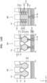
- FIG. 2B illustrates cross-sectional views taken along lines Y1-Y1', Y2-Y2', and Y3-Y3' of FIG. 1 .
- FIG. 3A is an enlarged view of a portion indicated by "EX1" of FIG. 2A
- FIG. 3B is an enlarged view of a portion indicated by "EX2" of FIG. 2B
- FIG. 3C is an enlarged view of a portion indicated by "EX3" of FIG. 2B .
- the integrated circuit device 100 may constitute a logic cell including a multi-bridge channel field-effect transistor (FET) (MBCFET) device.
- FET field-effect transistor
- the present inventive concept is not limited thereto, and the integrated circuit device 100 may include a two-dimensional material-based FET device, such as a planar FET device, a gate-all-around type FET device, a finFET device, and a MoS 2 semiconductor gate electrode.
- the integrated circuit device 100 may include an insulating substrate 182 including a plurality of fin structures FS defined by device isolation trenches 112T.
- the plurality of fin structures FS may extend in parallel to each other in the first horizontal direction (e.g., an X direction).
- the insulating substrate 182 may be made of silicon oxide, silicon nitride, or a combination thereof.
- a device isolation layer 112 filling the device isolation trench 112T may be disposed between the plurality of fin structures FS.
- the device isolation layer 112 may cover the bottom surface of the device isolation trench 112T and sidewalls of the plurality of fin structures FS.
- the top surfaces FT of the plurality of fin structures FS may be covered by lower insulating layers 114.
- the device isolation layer 112 may be formed of silicon oxide.
- a lower insulating layer 114 may be made of silicon oxide, silicon nitride, or a combination thereof.
- the lower insulating layer 114 may be made of a material having a dielectric constant of about 3.5 or more.
- a plurality of gate structures 140 may be disposed on the plurality of fin structures FS. According to some embodiments of the present inventive concept, the plurality of gate structures 140 may extend in parallel to each other in the second horizontal direction (e.g., a Y direction).
- each of a plurality of nanosheet stacks NSS may be placed on a top surface 114U of the lower insulating layer 114 in regions where the plurality of fin structures FS intersect with the plurality of gate structures 140.
- each of the plurality of nanosheet stacks NSS may face the top surface 114U of the lower insulating layer 114 at a position spaced apart from the lower insulating layer 114 in the vertical direction (e.g., a Z direction).
- the term "nanosheet” may refer to a conductive structure having a cross-section substantially perpendicular to a direction in which a current flows.
- the nanosheet may be understood as a concept including nanowires.
- on the insulating substrate 182 a plurality of nanosheet transistors may be formed in regions where the plurality of fin structures FS intersect with the plurality of gate structures 140.
- each of the plurality of nanosheet stacks NSS may include a first nanosheet N1, a second nanosheet N2, and a third nanosheet N3 overlapping on the lower insulating layer 114 in a vertical direction (e.g., the Z direction).
- the first nanosheet N1, the second nanosheet N2, and the third nanosheet N3 may have different distances in the vertical direction (e.g., the Z direction) from the upper surface 114U of the lower insulating layer 114.
- the plurality of gate structures 140 may wrap around the first nanosheet N1, the second nanosheet N2, and the third nanosheet N3 included in each of the nanosheet stacks NSS overlapping in the vertical direction (e.g., the Z direction), respectively. According to some embodiments of the present inventive concept, the plurality of gate structures 140 may at least partially surround the top surface 114U of the lower insulating layer 114 and sidewalls of the lower insulating layer 114.
- FIGS. 2A and 2B illustrate a case in which the planar shape of each of the nanosheet stacks NSS is approximately rectangular, the embodiments of the present inventive concept are not limited thereto.
- the nanosheet stacks NSS may have various planar shapes according to the planar shape of each of the fin structures FS and the gate structures 140.
- each of a plurality of nanosheet stacks NSS and each of a plurality of gate structures 140 are disposed on a fin structure FS, and each of a plurality of nanosheet stacks NSS is arranged in a line in a first horizontal direction (e.g., the X direction) on a fin structure FS.
- the number of nanosheet stacks NSS and the number of gate structures 140 placed on one fin structure FS are not particularly limited.
- each of the first nanosheet N1, the second nanosheet N2, and the third nanosheet N3 included in each of the nanosheet stacks NSS may function as a channel region.
- each of the first nanosheet N1, the second nanosheet N2, and the third nanosheet N3 may have a thickness selected from a range of about 4 nm to about 6 nm, but the present inventive concept is not limited thereto.
- the thickness of each of the first nanosheet N1, the second nanosheet N2, and the third nanosheet N3 is a magnitude in the vertical direction (e.g., the Z direction).
- each of the first nanosheet N1, the second nanosheet N2, and the third nanosheet N3 may have substantially the same thickness as each other in the vertical direction (e.g., the Z direction). According to some embodiments of the present inventive concept, at least one of the first nanosheet N1, the second nanosheet N2, and the third nanosheet N3 may have different thicknesses in the vertical direction (e.g., the Z direction) from each other. According to some embodiments of the present inventive concept, each of the first nanosheet N1, the second nanosheet N2, and the third nanosheet N3 included in the nanosheet stacks NSS may be formed of a Si layer, a SiGe layer, or a combination thereof.
- the first nanosheet N1, the second nanosheet N2, and the third nanosheet N3 included in one nanosheet stack NSS may have the same or similar sizes in the first horizontal direction (e.g., the X direction).
- at least some of the first nanosheet N1, the second nanosheet N2, and the third nanosheet N3 included in one nanosheet stack NSS may have different sizes in the first horizontal direction (e.g., the X direction) from each other.
- the nanosheet stack NSS may include at least one nanosheet, and the number of nanosheets constituting the nanosheet stack NSS is not particularly limited.
- the plurality of gate structures 140 may include a main gate portion 140M and a plurality of sub-gate portions 140S, respectively.
- the main gate portion 140M may extend in the second horizontal direction (e.g., the Y direction) while covering the top surfaces of the nanosheet stacks NSS.
- the plurality of sub-gate portions 140S may be integrally connected to the main gate portion 140M, and may be disposed between the first nanosheet N1 and the second nanosheet N2, between the second nanosheet N2 and the third nanosheet N3, and between the first nanosheet N1 and the lower insulating layer 114.
- the thickness of each of the plurality of sub-gate portions 140S may be less than the thickness of the main gate portion 140M.
- each of the plurality of gate structures 140 may be made of a metal, a metal nitride, a metal carbide, or a combination thereof.
- the metal may include, for example, Ti, W, Ru, Nb, Mo, Hf, Ni, Co, Pt, Yb, Tb, Dy, Er, Pd, and combinations thereof.
- the metal nitride may be selected from TiN and TaN.
- the metal carbide may be TiAlC.
- a gate dielectric layer 142 may be placed between a plurality of nanosheets N1, N2, and N3 constituting the nanosheet stack NSS and the gate structure 140.
- the gate dielectric layer 142 may include portions covering the surface of each of the plurality of nanosheets N1, N2, and N3, and portions covering the sidewalls of the main gate portion 140M.
- the main gate portion 140M may be disposed on the gate dielectric layer 142.
- the gate dielectric layer 142 may have a stacked structure of an interface layer and a high dielectric layer.
- the interface layer may include a low dielectric material layer with a dielectric constant of about 9 or less, for example, a silicon oxide layer, a silicon oxynitride layer, or a combination of it.
- the interface layer may be omitted.
- the high dielectric layer may be made of a material having a dielectric constant higher than the silicon oxide layer.
- the high dielectric layer may have a dielectric constant of about 10 to about 25.
- the high dielectric layer may be made of, for example, hafnium oxide, but the present inventive concept is not limited thereto.
- a first recess RS and a second recess RD may be formed on each of the plurality of fin structures FS.
- the second recess RD may be spaced apart from the first recess RS with the gate structure 140 adjacent to the first recess RS therebetween.
- a plurality of first source/drain regions 122 may be disposed in a plurality of first recesses RS, respectively, and a plurality of second source/drain regions 124 may be disposed in a plurality of second recesses RD, respectively.
- the first source/drain region 122 may be a source region
- the second source/drain region 124 may be a drain region.
- the first source/drain region 122 and the second source/drain region 124 may be formed of a semiconductor material.
- the semiconductor material may include semiconductors such as Si or Ge, or compound semiconductors such as SiGe, SiC, GaAs, InAs, InGaAs, or InP.
- the first source/drain regions 122 and the second source/drain regions 124 may each consist of a semiconductor layer doped with a p-type dopant.
- the p-type dopant may be selected from boron (B) and gallium (Ga).
- the first source/drain regions 122 and the second source/drain regions 124 may each consist of a semiconductor layer doped with an n-type dopant.
- the n-type dopant may be selected from phosphorus (P), arsenic (As), and antimony (Sb).
- the plurality of first source/drain regions 122 and the plurality of second source/drain regions 124 may be spaced apart from each other in the first horizontal direction (e.g., the X direction) with one gate structure 140 selected from the plurality of gate structures 140 therebetween, and may be arranged in the second horizontal direction (e.g., the Y direction).
- the plurality of first source/drain regions 122 and the plurality of second source/drain regions 124 may be arranged to cross each other in the second horizontal direction (e.g., the Y direction).
- the plurality of first source/drain regions 122 may each include a body portion 122a disposed between the plurality of nanosheet stacks NSS and a vertical extension portion 122b passing through the lower insulating layer 114 and at least partially penetrating the fin structure FS.
- the length of the lower insulating layer 114 may be limited in the first horizontal direction (e.g., the X direction) by the first source/drain region 122.
- the body portion 122a may have surfaces facing the first nanosheet N1, the second nanosheet N2, and the third nanosheet N3 included in the adjacent nanosheet stack NSS. According to some embodiments of the present inventive concept, the body portion 122a may be in contact with the first nanosheet N1, the second nanosheet N2, and the third nanosheet N3 that are included in the adjacent nanosheet stack NSS.
- the vertical extension portion 122b extends from the body portion 122a in the vertical direction (e.g., the Z direction) and may protrude from the bottom surface 114L of the lower insulating layer 114.
- the sidewall of the vertical extension portion 122b may include a portion facing the lower insulating layer 114 in the first horizontal direction (e.g., the X direction).
- the sidewall of the vertical extension portion 122b may include a portion facing the device isolation layer 112 in the second horizontal direction (e.g., the Y direction).
- the vertical extension portion 122b may penetrate the device isolation layer 112.
- the bottom surface 123 of the vertical extension portion 122b may have a vertical level lower than the bottom surface 114L of the lower insulating layer 114.
- the term "vertical level" used in this specification may be a distance in the vertical direction (Z direction or -Z direction) from the bottom surface 114L of the lower insulating layer 114.
- the vertical extension portion 122b may protrude from the bottom surface 114L of the lower insulating layer 114 by a first length h1.
- the body portion 122a may have a first width w1 in the first horizontal direction (e.g., the X direction), and the vertical extension portion 122b may have a second width w2 in the first horizontal direction (e.g., the X direction).
- the first width w1 of the body portion 122a may be substantially the same as the second width w2 of the vertical extension portion 122b.
- the first width w1 of the body portion 122a may be less than the second width w2 of the vertical extension portion 122b.
- the first width w1 of the body portion 122a may be greater than the second width w2 of the vertical extension portion 122b.
- the body portion 122a may have a third width w3 that is a width in the second horizontal direction (e.g., the Y direction), and the vertical extension portion 122b may have a fourth width w4 in the second horizontal direction (e.g., the Y direction).
- the third width w3 of the body portion 122a may be greater than the fourth width w4 of the vertical extension portion 122b.
- the plurality of second source/drain regions 124 may be disposed between the plurality of nanosheet stacks NSS on the lower insulating layer 114, respectively.
- the second source/drain regions 124 may penetrate the plurality of nanosheet stacks NSS.
- the plurality of second source/drain regions 124 may be in contact with the top surfaces 114U of the lower insulating layers 114, respectively.
- the plurality of second source/drain regions 124 may each have surfaces facing the first nanosheet N1, the second nanosheet N2, and the third nanosheet N3 that are included in the adjacent nanosheet stack NSS.
- the plurality of second source/drain regions 124 may be in contact with the first nanosheet N1, the second nanosheet N2, and the third nanosheet N3 included in the adjacent nanosheet stack NSS, respectively.
- the plurality of second source/drain regions 124 may be spaced apart from the fin structures FS with the lower insulating layers 114 therebetween, respectively.
- the lower insulating layer 114 according to some embodiments of the present inventive concept is placed between each of the plurality of fin structures FS and each of the plurality of second source/drain regions 124, preventing a short circuit between a lower contact structure 185, which connects a rear wiring structure 204 with the first source/drain region 122, and the second source/drain region 124 due to a process variation.
- a semiconductor epitaxial structure 126 surrounding the vertical extension portion 122b of the first source/drain region 122 may be disposed on the bottom surface 114L of the lower insulating layer 114. According to some embodiments of the present inventive concept, the semiconductor epitaxial structure 126 may contact the vertical extension portion 122b of the first source/drain region 122 and may be electrically connected to the first source/drain region 122. According to some embodiments of the present inventive concept, the semiconductor epitaxial structure 126 may have a structure partially penetrated in the vertical direction (e.g., the Z direction) by the vertical extension portion 122b of the first source/drain region 122.
- the semiconductor epitaxial structure 126 may be formed by epitaxially growing semiconductor materials in a part of the vertical extension portion 122b protruding on the bottom surface 114L of the lower insulating layer 114.
- the semiconductor materials may include group IV semiconductors such as Si or Ge, group IV-IV compound semiconductors such as SiGe or SiC, or group III-V compound semiconductors such as GaAs, InAs, or InP.
- the semiconductor epitaxial structure 126 may be formed of a p-type semiconductor layer doped with B or Ga.
- the semiconductor epitaxial structure 126 may be formed of an n-type semiconductor layer doped with P, As, or Sb.
- the semiconductor epitaxial structure 126 may include a first portion 126a with a positive profile having a width of the semiconductor epitaxial structure 126 in the horizontal direction that increases away from the bottom surface 114L of the lower insulating layer in the Z direction.
- the semiconductor epitaxial structure 126 may also include a second portion 126b extending from the first portion, and the second portion 126b has a negative profile such that the width of the semiconductor epitaxial structure 126 in the horizontal direction decreases away from the bottom surface 114L of the lower insulating layer in the Z direction.
- the sidewall of the semiconductor epitaxial structure 126 may have the positive profile in the first portion 126a and the negative profile in the second portion 126b.
- the profile of the semiconductor epitaxial structure 126 is due to the difference in the growth rate of the epitaxial layer according to the crystal plane of the vertical extension portion 122b of the first source/drain region 122.
- the epitaxial layer may grow at a faster rate in the ⁇ 110> crystal plane than in the ⁇ 100> crystal plane of the vertical extension portion 122b, and at a slower rate in each of the ⁇ 311> crystal plane and ⁇ 111> crystal plane than in the ⁇ 100> crystal plane thereof.
- the semiconductor epitaxial structure 126 grows a semiconductor material from the vertical extension portion 122b, which is protruding from the bottom surface 114L of the lower insulating layer 114, by using a growth rate difference of the epitaxial layers according to the crystal planes and may thus have a profile having an expanded width in the horizontal direction (e.g., the X direction and/or Y direction).
- the semiconductor epitaxial structure 126 may have a third portion 126c having a maximum horizontal width between the first portion 126a and the second portion 126b. According to some embodiments of the present inventive concept, the horizontal width of the third portion 126c of the semiconductor epitaxial structure 126 may be greater than the horizontal width of the vertical extension portion 122b of the first source/drain region 122.
- the fifth width w5, which is the width of the third portion 126c of the semiconductor epitaxial structure 126, in the first horizontal direction (e.g., the X direction) may be greater than the second width w2, which is the width of the vertical extension portion 122b of the first source/drain region 122, in the first horizontal direction (e.g., the X direction).
- the sixth width w6, which is the width of the third portion 126c of the semiconductor epitaxial structure 126, in the second horizontal direction (e.g., the Y direction) may be greater than the fourth width w4, which is the width of the vertical extension portion 122b of the first source/drain region 122, in the second horizontal direction (e.g., the Y direction).
- the first portion 126a, the second portion 126b, and the third portion 126c shown in FIGS. 2A and 3A refer to different portions from the first portion 126a, the second portion 126b, and the third portion 126c shown in FIGS. 2B and 3B .
- the semiconductor epitaxial structure 126 may include the first portion 126a with the positive profile, the second portion 126b with the negative profile, and the third portion 126c between the first portion 126a and the second portion 126b, in cross-sections ( FIGS. 2A and 3A ) in the first horizontal direction (e.g., the X direction).
- the semiconductor epitaxial structure 126 may additionally include the first portion 126a with the positive profile, the second portion 126b with the negative profile, and the third portion 126c between the first portion 126a and the second portion 126b, in cross-sections ( FIGS. 2B and 3B ) in the second horizontal direction (e.g., the X direction).
- the semiconductor epitaxial structure 126 may have a bottom surface 126L opposite to a portion of the semiconductor epitaxial structure 126 that is in contact with the lower insulating layer 114. According to some embodiments of the present inventive concept, the bottom surface 126L of the semiconductor epitaxial structure 126 may be disposed at a vertical level lower than the bottom surface 123 of the first source/drain region 122. According to some embodiments of the present inventive concept, the bottom surface 126L of the semiconductor epitaxial structure 126 may be disposed at a vertical level lower than the bottom surface 114L of the lower insulating layer 114 by a second height h2.
- the bottom surface 126L of the semiconductor epitaxial structure 126 may be disposed at a vertical level lower than the bottom surface 112L of the device isolation layer 112 by a third height h3.
- the second height h2 may be greater than the third height h3.
- the insulating substrate 182 may have a rear surface 182B opposite to a fin top surface FT.
- a lower contact structure 185 penetrates a portion of the insulation substrate 182 in the vertical direction (e.g., the Z direction) and contacts the semiconductor epitaxial structure 126.
- a lower silicide layer 183 may be formed between the lower contact structure 185 and the semiconductor epitaxial structure 126.
- the lower contact structure 185 may include a conductive barrier 184a and a contact plug 184b.
- the conductive barrier 184a that at least partially surrounds the top surface and side surfaces of the contact plug 184b, and may be disposed on the top surface and side surfaces of the contact plug 184b.
- the conductive barrier 184a may be in contact with the top surface and side surfaces of the contact plug 184b.
- the conductive barrier 184a may be placed between the lower silicide layer 183 and the contact plug 184b.
- the contact plug 184b may be made of molybdenum (Mo), copper (Cu), tungsten (W), cobalt (Co), ruthenium (Ru), manganese (Mn), titanium (Ti), tantalum (Ta), aluminum (Al), a combination thereof, or an alloy thereof, but the present inventive concept is not limited thereto.
- the conductive barrier 184a may be made of metal or metal nitride.
- the conductive barrier 184a may be formed of Ti, Ta, W, TiN, TaN, WN, WCN, TiSiN, TaSiN, WSiN, or a combination thereof, but the present inventive concept is not limited thereto.
- the lower silicide layer 183 may include a metal formed of Ti, W, Ru, Nb, Mo, Hf, Ni, Co, Pt, Yb, Tb, Dy, Er, or Pd.
- the lower silicide layer 183 may be made of titanium silicide, but the present inventive concept is not limited thereto.
- the lower contact structure 185 may be formed of a single structure including a semiconductor material.
- the semiconductor material may include Si, Ge, or SiGe, and may include doped polysilicon.
- the present inventive concept is not limited to, and for example, the lower contact structure 185 may be a multilayer structure.
- a first lower insulating layer 192 and a second lower insulating layer 202 may be sequentially stacked on the rear surface 182B of the insulating substrate 182.
- the first lower insulating layer 192 and the second lower insulating layer 202 may be formed of a silicon oxide layer, a silicon nitride layer, a silicon carbide layer, a low dielectric layer, or a combination thereof, respectively.
- the low dielectric layer is fluorine-doped silicon oxide, organosilicate glass, carbondoped oxide, porous silicon oxide, porous organosilicate glass, spin-on organic polymeric dielectric, spin-on silicon based polymeric dielectric, or a combination thereof, but the present inventive concept is not limited to the examples.
- the rear wiring structure 204 may extend in the first horizontal direction (e.g., the X direction) and may be disposed to penetrate the second lower insulation layer 202.
- the rear wiring structure 204 may include a power delivery network configured to apply power voltage and ground voltage to the nanosheet transistor.
- the rear wiring structure 204 may be formed of Co, W, Cu, Ru, Mn, Ti, Ta, TiN, TaN, or a combination thereof, but the present inventive concept is not limited thereto.
- the rear wiring structure 204 may be connected to the lower contact structure 185 through a lower via contact 194 that is in contact with the lower contact structure 185.
- the lower via contact 194 may include of molybdenum (Mo) or tungsten (W), but the present inventive concept is not limited thereto.
- the rear wiring structure 204 may be configured to be electrically connected to the first source/drain region 122 through the lower via contact 194, the lower contact structure 185, the lower silicide layer 183, and the semiconductor epitaxial structure 126.
- the lower contact structure 185 and the lower via contact 194 may constitute a lower contact for electrically connecting the rear wiring structure 204 with the first source/drain region 122.
- the semiconductor epitaxial structure 126 may secure a contact margin of the lower contact structure 185 connected to the semiconductor epitaxial structure 126, while including a third portion 126c with an extended horizontal width.
- the semiconductor epitaxial structure 126 is placed in the insulation substrate 182.
- the lower contact structure 185 penetrates the insulation substrate 182 and is connected to the semiconductor epitaxial structure 126.
- a separate insulation liner for electrical insulation between the lower contact structure 185 and the semiconductor substrate may be desirable, but the insulation liner for electrical insulation may be omitted from the integrated circuit device 100 according to some embodiments of the present inventive concept.
- a gate dielectric layer 142 may be placed between the nanosheet stack NSS and the gate structure 140. According to some embodiments of the present inventive concept, both sidewalls of each of the plurality of sub-gate portions 140S included in the plurality of gate structures 140 may be spaced apart from the first and second source/drain regions 122 and 124 with the gate dielectric layer 142 therebetween. According to some embodiments of the present inventive concept, the gate dielectric layer 142 may be placed between the sub-gate portion 140S of the gate structure 140 and each of the first nanosheet N1, the second nanosheet N2, and the third nanosheet N3, and between the sub-gate portion 140S of the gate structure 140 and each of the first and second source/drain regions 122 and 124.
- the gate dielectric layer 142 may have a stacked structure of an interface dielectric layer and a high dielectric layer.
- the interface dielectric layer may be formed of a low dielectric material layer having a dielectric constant of about 9 or less, for example, a silicon oxide layer, a silicon oxynitride layer, or a combination thereof.
- the interface dielectric layer may be omitted.
- the high dielectric layer may be made of a material having a higher dielectric constant than that of a silicon oxide layer.
- the high dielectric layer may have a dielectric constant of about 10 to about 25.
- the high dielectric layer may be made of hafnium oxide, but the present inventive concept is not limited thereto.
- a top surface of each of the gate dielectric layer 142 and the gate structure 140 may be covered with a capping insulating layer 144.
- the capping insulating layer 144 may be formed of a silicon nitride layer.
- both sidewalls of each of the gate structure 140 and the capping insulating layer 144 may be covered with an outer insulating spacer 108.
- the outer insulating spacer 108 may cover sidewalls of a main gate portion 140M while on the top surface of each of the plurality of nanosheet stacks NSS.
- the outer insulating spacer 108 may be spaced apart from the gate structure 140 with the gate dielectric layer 142 therebetween.
- a recess-side insulating spacer 116 which covers a part of the sidewall of the vertical extension portion 122b of the plurality of first source/drain regions 122 and the sidewall of the lower insulating layer 114, may be disposed on the top surface of the device isolation layer 112.
- the recess-side insulating spacer 116 may be integrally connected to the outer insulating spacer 108.
- the sidewall of the vertical extension portion 122b of the first source/drain region 122 may be covered by the recess-side insulating spacer 116 and the device isolation layer 112 in the second horizontal direction (e.g., the Y direction).
- the vertical extension portion 122b of the first source/drain region 122 may extend in the vertical direction (e.g., the Z direction) in a space limited by the recess-side insulating spacer 116 and the device isolation layer 112.
- each of the outer insulating spacer 108 and the recess-side insulating spacer 116 may be formed of silicon nitride, silicon oxide, SiCN, SiBN, SiON, SiOCN, SiBCN, SiOC, or a combination thereof.
- SiCN silicon nitride
- SiBN silicon oxide
- SiON silicon oxide
- SiOCN SiBCN
- SiOC silicon oxide
- SiBCN silicon oxide
- SiOC silicon oxide
- SiCN silicon oxide
- SiBN SiBN
- SiON SiOCN
- SiBCN SiOC
- an upper silicide layer 152 may be formed on a top surface of each of the plurality of second source/drain regions 124.
- the upper silicide layer 152 may include a metal formed of W, Ru, Nb, Mo, Hf, Ni, Co, Pt, Yb, Tb, Dy, Er, or Pd.
- the upper silicide layer 152 may be made of titanium silicide, but the present inventive concept is not limited thereto.
- the plurality of first source/drain regions 122, the plurality of second source/drain regions 124, and the plurality of outer insulating spacers 108 may be covered with insulating liners 132 on the insulating substrate 182.
- an inter-gate insulating layer 134 may be disposed on the insulating liner 132.
- the insulating liner 132 may be omitted.
- the inter-gate insulating layer 134 may be in contact with the plurality of first source/drain regions 122 and the plurality of second source/drain regions 124.
- the insulating liners 132 may be formed of silicon nitride, SiCN, SiBN, SiON, SiOCN, SiBCN, or a combination thereof, but the present inventive concept is not limited thereto.
- the inter-gate insulating layer 134 may be formed of a silicon oxide layer, but present inventive concept is not limited thereto.
- a source/drain contact structure 154 may be disposed on each of the plurality of second source/drain regions 124. According to some embodiments of the present inventive concept, the source/drain contact structure 154 may penetrate the inter-gate insulation layer 134 and the insulation liner 132 in the vertical direction (e.g., the Z direction) to contact the upper silicide layer 152. According to some embodiments of the present inventive concept, the plurality of second source/drain regions 124 may be configured to be electrically connected to the source/drain contact structures 154 through the upper silicide layers 152, respectively.
- the source/drain contact structure 154 may include a conductive barrier 153a and a contact plug 153b sequentially stacked on the second source/drain region 124.
- the conductive barrier 153a at least partially surrounds the bottom and side surfaces of the contact plug 153b and is disposed on the bottom and side surfaces of the contact plug 153b.
- the conductive barrier 153a may be in contact with the bottom and side surfaces of the contact plug 153b.
- the conductive barrier 153a may be placed between the upper silicide layer 152 and the contact plug 153b.
- the conductive barrier 153a may be made of metal or metal nitride. According to some embodiments of the present inventive concept, the conductive barrier 153a may be formed of Ti, Ta, W, TiN, TaN, WN, WCN, TiSiN, TaSiN, WSiN, or a combination thereof, but the present inventive concept is not limited thereto.
- the contact plug 153b may be made of, for example, molybdenum (Mo), copper (Cu), tungsten (W), cobalt (Co), ruthenium (Ru), manganese (Mn), titanium (Ti), tantalum (Ta), aluminum (Al), a combination thereof, or an alloy thereof, but the present inventive concept is not limited thereto.
- the top surface of each of the source/drain contact structure 154, the capping insulating layer 144, and the inter-gate insulating layer 134 may be covered with a first upper insulating layer 163.
- the first upper insulating layer 163 may include an etching stop layer 162a and an interlayer insulating layer 162b, which are stacked sequentially on the source/drain contact structure 154, the capping insulating layer 144, and the inter-gate insulating layer 134.
- the etching stop layer 162a may be formed of silicon carbide (SiC), SiN, nitrogen-doped silicon carbide (SiCN), SiOC, AlN, AlON, AlO, AlOC, or a combination thereof.
- the interlayer insulating layer 162b may be formed of an oxide layer, a nitride layer, an ultra low-k (ULK) layer having an ultra low dielectric constant K of about 2.2 to about 2.4, or a combination thereof.
- the interlayer insulating layer 162b may include a tetraethylorthosilicate (TEOS) layer, a high density plasma (HDP) oxide layer, a boro-phospho-silicate glass (BPSG) layer, a flowable chemical vapor deposition (FCVD) oxide layer, a SiON layer, a SiN layer, a SiOC layer, a SiCOH layer, or a combination thereof, but the present inventive concept is not limited thereto.
- TEOS tetraethylorthosilicate
- HDP high density plasma
- BPSG boro-phospho-silicate glass
- FCVD flowable chemical vapor deposition
- a source/drain via contact 164 may be disposed on the source/drain contact structure 154.
- the source/drain via contact 164 may penetrate the first upper insulating layer 163 to be in contact with the source/drain contact structure 154.
- the plurality of second source/drain regions 124 may be configured to be electrically connected to the source/drain via contact 164 through the upper silicide layer 152 and the source/drain contact structure 154, respectively.
- the bottom surface of the source/drain via contact 164 may be in contact with the top surface of the source/drain contact structure 154.
- the source/drain via contact 164 may be made of molybdenum (Mo) or tungsten (W) but is not limited thereto.
- a gate contact 166 may be disposed on the gate structure 140.
- the gate contact 166 may be configured to penetrate the first upper insulating layer 163 and the capping insulating layer 144 in the vertical direction (e.g., the Z direction) to be connected to the gate structure 140.
- the bottom surface of the gate contact 166 may be disposed on the top surface of the gate structure 140.
- the bottom surface of the gate contact 166 may be in contact with the top surface of the gate structure 140.
- the gate contact 166 may include a contact plug made of, for example, molybdenum (Mo), copper (Cu), tungsten (W), cobalt (Co), ruthenium (Ru), manganese (Mn), titanium (Ti), tantalum (Ta), aluminum (Al), a combination thereof, or an alloy thereof, but the constituent material of the gate contact 166 is not limited to those described above.
- the gate contact 166 may further include a conductive barrier pattern surrounding a portion of the contact plug.
- the conductive barrier pattern included in the gate contact 166 may be made of a metal or a metal nitride.
- the conductive barrier pattern may be formed of Ti, Ta, W, TiN, TaN, WN, WCN, TiSiN, TaSiN, WSiN, or a combination thereof, but the present inventive concept is not limited thereto.
- the top surfaces of the first upper insulating layer 163 and the source/drain via contact 164 may be covered by a second upper insulating layer 172.
- the second upper insulating layer 172 may include a tetraethylorthosilicate (TEOS) layer, a high density plasma (HDP) oxide layer, a boro-phospho-silicate glass (BPSG) layer, a flowable chemical vapor deposition (FCVD) oxide layer, a SiON layer, a SiN layer, a SiOC layer, a SiCOH layer, or a combination thereof, but the present inventive concept is not limited thereto.
- TEOS tetraethylorthosilicate
- HDP high density plasma
- BPSG boro-phospho-silicate glass
- FCVD flowable chemical vapor deposition
- the front wiring structure 174 may be disposed to penetrate the second upper insulating layer 172. According to some embodiments of the present inventive concept, the front wiring structure 174 may be connected to the source/drain via contact 164 and the gate contact 166. According to some embodiments of the present inventive concept, the front wiring structure 174 may be made of molybdenum (Mo), copper (Cu), tungsten (W), cobalt (Co), ruthenium (Ru), manganese (Mn), titanium (Ti), tantalum (Ta), aluminum (Al), a combination thereof, or an alloy thereof, but the present inventive concept is not limited thereto. According to some embodiments of the present inventive concept, the source/drain contact structure 154 and the source/drain via contact 164 may constitute an upper contact to electrically connect the front wiring structure 174 with the second source/drain region 124.
- FIGS. 4A to 16B are cross-sectional views illustrating a method of manufacturing an integrated circuit device according to an embodiment of the present inventive concept in a process sequence, and are cross-sectional views taken along an X-X' line, a Y1-Y1' line, a Y2-Y2' line, and a Y3-Y3' line of FIG. 1 . More specifically, FIGS.
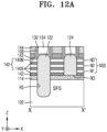
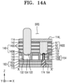
- FIGS. 4A , 5A , 6A , 7A , 8A , 9A , 10A , 11A , 12A , 13A , 14A , 15A , and 16A are cross-sectional views respectively illustrating cross-sectional structures according to a process sequence of a portion corresponding to a cross-section taken along line X-X' of FIG. 1 .
- FIGS. 4A , 5A , 6A , 7A , 8A , 9A , 10A , 11A , 12A , 13A , 14A , 15A , and 16A are cross-sectional views respectively illustrating cross-sectional structures according to a process sequence of a portion corresponding to a cross-section taken along line X-X' of FIG. 1 .
- 4B , 5B , 6B , 7B , 8B , 9B , 10B , 11B , 12B , 13B , 14B , 15B , and 16B are cross-sectional views respectively illustrating cross-sectional structures according to a process sequence corresponding to a portion corresponding to a cross-section of lines Y1-Y1', Y2-Y2', and Y3-Y3' of FIG. 1 .
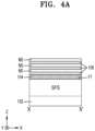
- a first sacrificial semiconductor layer 104 may be formed on a sacrificial substrate 102, and then a plurality of second sacrificial semiconductor layers 106 and a plurality of nanosheet semiconductor layers NS may be alternately stacked on the first sacrificial semiconductor layer 104.
- the sacrificial substrate 102 may include a semiconductor such as Si or Ge, or a compound semiconductor such as SiGe, SiC, GaAs, InAs, InGaAs, or InP.
- a semiconductor such as Si or Ge
- a compound semiconductor such as SiGe, SiC, GaAs, InAs, InGaAs, or InP.
- SiGe, SiC, GaAs, InAs, InGaAs, or InP refer to materials composed of elements included in each term, and are not chemical formulae representing a stoichiometric relationship.
- the first sacrificial semiconductor layer 104, the plurality of second sacrificial semiconductor layers 106, and the plurality of nanosheet semiconductor layers NS may be formed of semiconductor materials having different etching selectivities.
- the plurality of nanosheet semiconductor layers NS may be formed of a Si layer, and the first sacrificial semiconductor layer 104 and the plurality of second sacrificial semiconductor layers 106 may be formed of a SiGe layer.
- the first sacrificial semiconductor layer 104 and the plurality of second sacrificial semiconductor layers 106 may have different concentrations of Ge.
- the SiGe layer constituting the first sacrificial semiconductor layer 104 may have a first Ge concentration
- the SiGe layer constituting the plurality of second sacrificial semiconductor layers 106 may have a second Ge concentration.
- the first Ge concentration in the first sacrificial semiconductor layer 104 may be constant
- the second Ge concentration in the plurality of second sacrificial semiconductor layers 106 may be constant.
- the first Ge concentration of the first sacrificial semiconductor layer 104 may be greater than the second Ge concentration of the plurality of second sacrificial semiconductor layers 106.
- the first Ge concentration of the first sacrificial semiconductor layer 104 may be about 50 at% or more or about 60 at% or more.
- the second Ge concentration of each of the plurality of second sacrificial semiconductor layers 106 may range from about 5 at% to about 40 at%.
- each of the sacrificial substrate 102, the first sacrificial semiconductor layer 104, the plurality of second sacrificial semiconductor layers 106, and the plurality of nanosheet semiconductor layers NS may be etched to form a device isolation trench 112T.
- a plurality of sacrificial fin structures SFS may be defined by the device isolation trench 112T.
- the plurality of sacrificial fin structures SFS may extend in parallel to each other in the first horizontal direction (e.g., the X direction).
- a stack structure of the first sacrificial semiconductor layer 104, the plurality of second sacrificial semiconductor layer 106, and the plurality of nanosheet semiconductor layers NS may remain on the top surface FT of each of the plurality of sacrificial fin structures SFS.
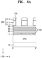
- a device isolation layer 112 may be formed to cover both sidewalls of each of the plurality of sacrificial fin structures SFS and fill the device isolation trench 112T of FIG. 4B .
- the top surface of the device isolation layer 112 may be at the same or similar level at which the top surface FT of each of the plurality of sacrificial fin structures SFS is located.
- a plurality of dummy gate structures DSG and outer insulating spacers 108 covering both sidewalls of the plurality of dummy gate structures DSG may be formed.
- the plurality of dummy gate structures DSG may extend in parallel to each other in the second horizontal direction (e.g., the Y direction) at positions corresponding to the plurality of gate structures 140 illustrated in FIG. 1 .
- the plurality of dummy gate structures DGS may each have a structure in which a dummy oxide layer D112, a dummy gate layer D114, and a capping layer D116 are stacked in order.
- the dummy gate layer D114 may be formed of a polysilicon layer
- the capping layer D116 may be formed of a silicon nitride layer.
- a lower insulating layer 114 may be formed in a space in which the first sacrificial semiconductor layer 104 was disposed.
- the first sacrificial semiconductor layer 104 may be selectively removed by utilizing the different etching selectivities between the first sacrificial semiconductor layer 104, the second sacrificial semiconductor layer 106, and the plurality of nanosheet semiconductor layers NS.
- a liquid or gaseous etchant may be used to selectively remove the first sacrificial semiconductor layer 104.
- the etchant may be formed of, for example, a CH 3 COOH-based etchant, for example, an etchant formed of a mixture of CH 3 COOH, HNO 3 , and HF, or an etchant formed of a mixture of CH 3 COOH, H 2 O 2 , and HF, but the present inventive concept is not limited thereto.
- the lower insulating layer 114 may be formed through an atomic layer deposition (ALD) process, a chemical vapor deposition (CVD), a plasma-enhanced CVD (PECVD) process, and a low-pressure CVD (LPCVD) process, but the present inventive concept is not limited to the above.
- ALD atomic layer deposition
- CVD chemical vapor deposition
- PECVD plasma-enhanced CVD
- LPCVD low-pressure CVD
- a spacer layer p116 covering the top surfaces of the dummy gate structures DGS, the outer insulating spacers 108, and the device isolation layer 112, both sidewalls of the lower insulating layer 114, both sidewalls of the plurality of nanosheet semiconductor layers NS, and both sidewalls of the plurality of second sacrificial semiconductor layers 106, which are not covered by the dummy gate structures DGS, may be formed.
- the spacer layer p116 may be formed of SiOCN.
- the spacer layer p116 may include a SiOCN layer covering the outer insulating spacer 108 and an oxide layer covering the SiOCN layer.
- the top surface of the device isolation layer 112 is at the same vertical level as the top surfaces FT of the plurality of sacrificial fin structures SFS and the device isolation layer 112 covers both sidewalls of each of the plurality of sacrificial fin structures SFS, it has been illustrated that the spacer layer p116 does not contact the plurality of sacrificial fin structures SFS, but the present inventive concept is not limited thereto.
- the top surface of the device isolation layer 112 may be lower than the top surfaces FT of the plurality of sacrificial fin structures SFS, and the spacer layer p116 may cover a portion of both exposed sidewalls of the plurality of sacrificial fin structures SFS.
- the plurality of dummy gate structures DGS and the outer insulating spacers 108 may be used as etching masks to etch a portion of each of the plurality of second sacrificial semiconductor layers 106, the plurality of nanosheet semiconductor layers NS, the lower insulating layers 114, and portions of the plurality of sacrificial fin structures SFS to thereby divide the plurality of nanosheet semiconductor layers NS into the plurality of nanosheet stacks NSS including the first nanosheet N1, the second nanosheet N2, and the third nanosheet N3, respectively, and form a first recess RS and/or a second recess RD on an upper portion of each of the plurality of sacrificial fin structures SFS.
- the spacer layer p116 may be partially etched together to form a recess-side insulating spacer 116 disposed adjacent to the first recess RS and the second rece
- the first recess RS may be formed by etching a portion of each of the plurality of second sacrificial semiconductor layers 106, the plurality of nanosheet semiconductor layers NS, the lower insulating layers 114, and portions of the plurality of sacrificial fin structures SFS.
- the bottom surface of the first recess RS may be formed to be lower than the bottom surface 114L of the lower insulating layer 114.
- the second recess RD may be formed by etching a portion of each of the plurality of second sacrificial semiconductor layers 106 and the plurality of nanosheet semiconductor layers NS, and the top surfaces 114U of the lower insulating layers 114 may be exposed through the second recess RD.
- the first recess RS may be formed by etching a portion of each of the plurality of second sacrificial semiconductor layers 106 and the plurality of nanosheet semiconductor layers NS so that the top surfaces 114U of the lower insulating layers 114 are exposed, disposing a mask pattern covering the second recess RD, and additionally etching a portion of each of the lower insulating layers 114 and a portion of each of the plurality of sacrificial fin structures SFS.
- dry etching, wet etching, or a combination thereof may be used to form, for example, the first recess RS and the second recess RD.
- the first source/drain regions 122 filling the first recesses RS and the second source/drain regions 124 filling the second recesses RD may be formed.
- raw materials including element semiconductor precursors may be used to perform a low-pressure chemical vapor deposition (LPCVD) process, a selective epitaxial growth (SEG) process, or a cyclic deposition and etching process (CDE).
- LPCVD low-pressure chemical vapor deposition
- SEG selective epitaxial growth
- CDE cyclic deposition and etching process
- the first and second source/drain regions 122 and 124 may be formed by epitaxially growing semiconductor materials from sidewalls of each of the first nanosheet N1, the second nanosheet N2, and the third nanosheet N3 included in each of the plurality of nanosheet stacks NSS.
- an insulating liner 132 is formed to cover the resultant structure of FIGS. 9A and 9B , an inter-gate insulating layer 134 is formed on the insulating liner 132, and a portion of each of the insulating liner 132 and the inter-gate insulating layer 134 is etched to expose the top surface of the capping layer D116. Thereafter, the capping layer D116 is removed, and the plurality of outer insulating spacers 108, the insulating liner 132, and the inter-gate insulating layer 134 are planarized to expose the top surface of the dummy gate layer D114.
- a gate space GS may be prepared by removing the dummy gate layer D114 and the oxide layer D112 thereunder from the results of FIGS. 10A and 10B , and the plurality of nanosheet stacks NSS may be exposed through the gate space GS. Thereafter, the plurality of second sacrificial semiconductor layers 106 remaining on the lower insulating layers 114 are removed through the gate space GS that is on each of the nanosheet stacks NSS and extend up to the space between the nanosheets N1 and N2, and N2 and N3 of the plurality of nanosheets N1, N2, and N3 and the space between the first nanosheet N1 and the top surface of the lower insulation layer 114.
- differences in etching selectivities between the first nanosheet N1, the second nanosheet N2, and the third nanosheet N3 and the plurality of second sacrificial semiconductor layers 106 may be used to selectively remove the plurality of second sacrificial semiconductor layers 106.
- a liquid or gaseous etchant may be used to selectively remove the plurality of second sacrificial semiconductor layers 106.
- a CH 3 COOH-based etchant for example, an etchant formed of a mixture of CH 3 COOH, HNO 3 , and HF, or an etchant formed of a mixture of CH 3 COOH, H 2 O 2 , and HF, may be used, but the etchant is not limited to those described above.
- the gate dielectric layer 142 covering the exposed surfaces of the plurality of nanosheets N1, N2, and N3 may be formed.
- the gate dielectric layer 142 may be formed to conformally cover the surfaces of the lower insulating layers 114, which are exposed through the gate space GS, the surfaces of the outer insulating spacers 108, and the surfaces of the inter-gate insulating layers 134.
- the gate dielectric layer 142 may be formed through an ALD process.
- a gate structure 140 covering the top surface of the inter-gate insulating layer 134 while filling the gate space GS on the gate dielectric layer 142, and a capping insulating layer 144 covering the top surface of each of the gate structure 140 and the gate dielectric layer 142 in the gate space GS may be formed.
- the capping insulating layer 144, the gate dielectric layer 142, the outer insulating spacer 108, the insulating liner 132, and the inter-gate insulating layer 134 may be planarized, and thus, the top surface of the inter-gate insulating layer 134 may be exposed.
- portions of the gate structure 140 that are covering the top surface of the inter-gate insulating layer 134 may be removed.
- a source/drain contact hole exposing the second source/drain region 124 may be formed through the insulating liner 132 and the inter-gate insulating layer 134, and then some areas of the second source/drain region 124 may be removed by an anisotropic etching process through the source/drain contact hole to thereby have the source/drain contact hole extend toward the sacrificial substrate 102. Thereafter, the upper silicide layer 152 may be formed on the second source/drain region 124 exposed from the bottom side of the source/drain contact hole. Thereafter, the source/drain contact structure 154 including the conductive barrier 153a and the contact plug 153b may be formed on the upper silicide layer 152.
- the first upper insulation layer 163 may be formed by sequentially forming an etch stop layer 162a and an interlayer insulation layer 162b covering the top surface of each of the inter-gate insulation layer 134, the source/drain contact structure 154, and the capping insulation layer 144.
- the gate contact 166 connected to the gate structure 140 may be formed by penetrating, in the vertical direction (e.g., the Z direction), the first upper insulating layer 163 and the capping insulating layer 144.
- the source/drain via contact 164 may be formed by penetrating the first upper insulating layer 163 to be connected to the source/drain contact structure 154.
- the sequence of forming the source/drain via contact 164 and the gate contact 166 is not particularly limited.
- a second upper insulating layer 172 covering the first upper insulating layer 163 and a front wiring structure 174, which is connected to the source/drain via contact 164 and the gate contact 166 by penetrating the second upper insulating layer 172, may be formed.
- the front wiring structure 174 may extend in the horizontal direction (e.g., the X direction and/or Y direction) on the first upper insulating layer 163.
- FIGS. 14A and 14B after a carrier substrate is attached on the second upper insulating layer 172, the resultant structure of FIGS. 13A and 13B is flipped, and then an etching process is performed on the rear surface 102b of the sacrificial substrate 102 to remove the sacrificial substrate 102, thereby forming a backside recess BRS.
- a buffer layer may be disposed between the carrier substrate and the second upper insulating layer 172.
- the bottom surface 112L and the side surface 112S of the device isolation layer 112, and the bottom surface 114L of the lower insulating layer 114 may be exposed through the backside recess BRS.
- the vertical extension portion 122b of the first source/drain region 122 protruding above the bottom surface 114L of the lower insulating layer 114 may be exposed through the backside recess BRS.
- the second source/drain region 124 may be covered by the lower insulating layer 114 and might not be exposed through the backside recess BRS.
- a semiconductor epitaxial structure 126 may be formed by epitaxially growing a semiconductor material from the vertical extension portion 122b of the exposed first source/drain region 122.
- the vertical extension portion 122b protrudes above the bottom surface 114L of the lower insulating layer 114, and the semiconductor epitaxial structure 126 may be formed to have an extended structure in the horizontal direction (e.g., the X direction and/or the Y direction).
- the insulating substrate 182 may be formed to cover the exposed portions of the device isolation layer 112, the lower insulating layer 114, and the semiconductor epitaxial structure 126.
- a lower contact hole which exposes the semiconductor epitaxial structure 126 by penetrating the insulating substrate 182 may be formed and then, a portion of the semiconductor epitaxial structure 126 may be removed through the lower contact hole by an anisotropic etching process so that the lower contact hole may extend longer toward the first source/drain region 122.
- a lower silicide layer 183 may be formed on the semiconductor epitaxial structure 126 that is exposed from the bottom side of the lower contact hole.
- a lower contact structure 185 including a conductive barrier 184a and a contact plug 184b may be formed on the lower silicide layer 183.
- a first lower insulating layer 192 which covers the rear surface 182B of the insulating substrate 182 and the lower contact structure 185, may be formed.
- a lower via contact 194 connected to the lower contact structure 185 may be formed by penetrating the first lower insulating layer 192 in the vertical direction (e.g., the Z direction).
- a second lower insulating layer 202 which covers the first lower insulating layer 192, and a rear wiring structure 204, which is connected to the lower via contact 194 by penetrating the second lower insulating layer 202, may be formed.
- the integrated circuit device 100 of FIG. 1 according to FIGS. 2A and 2B may be obtained.
Landscapes
- Insulated Gate Type Field-Effect Transistor (AREA)
- Thin Film Transistor (AREA)
- Metal-Oxide And Bipolar Metal-Oxide Semiconductor Integrated Circuits (AREA)
- Semiconductor Memories (AREA)
- Element Separation (AREA)
Applications Claiming Priority (1)
| Application Number | Priority Date | Filing Date | Title |
|---|---|---|---|
| KR1020230005636A KR20240113274A (ko) | 2023-01-13 | 2023-01-13 | 집적회로 소자 및 이의 제조 방법 |
Publications (3)
| Publication Number | Publication Date |
|---|---|
| EP4401144A2 true EP4401144A2 (de) | 2024-07-17 |
| EP4401144A3 EP4401144A3 (de) | 2024-10-09 |
| EP4401144B1 EP4401144B1 (de) | 2026-03-11 |
Family
ID=89121777
Family Applications (1)
| Application Number | Title | Priority Date | Filing Date |
|---|---|---|---|
| EP23214900.5A Active EP4401144B1 (de) | 2023-01-13 | 2023-12-07 | Integrierte schaltungsanordnung mit einem feldeffekttransistor und verfahren zu deren herstellung |
Country Status (6)
| Country | Link |
|---|---|
| US (1) | US20240243188A1 (de) |
| EP (1) | EP4401144B1 (de) |
| JP (1) | JP2024100724A (de) |
| KR (1) | KR20240113274A (de) |
| CN (1) | CN118352356A (de) |
| TW (1) | TW202429714A (de) |
Cited By (1)
| Publication number | Priority date | Publication date | Assignee | Title |
|---|---|---|---|---|
| EP4608090A1 (de) * | 2024-02-21 | 2025-08-27 | Intel Corporation | Integrierte schaltungsstruktur mit direktem rückseiten-source- oder drain-kontakt, der durch silicium-germanium-ätzstopp aktiviert wird |
Family Cites Families (5)
| Publication number | Priority date | Publication date | Assignee | Title |
|---|---|---|---|---|
| US11349004B2 (en) * | 2020-04-28 | 2022-05-31 | Taiwan Semiconductor Manufacturing Co., Ltd. | Backside vias in semiconductor device |
| DE102020122828B4 (de) * | 2020-05-27 | 2022-08-11 | Taiwan Semiconductor Manufacturing Co., Ltd. | Halbleitervorrichtungen, aufweisend rückseitige durchkontaktierungen und verfahren zu deren bildung |
| US11626494B2 (en) * | 2020-06-17 | 2023-04-11 | Taiwan Semiconductor Manufacturing Co., Ltd. | Epitaxial backside contact |
| US12557677B2 (en) * | 2021-01-18 | 2026-02-17 | Samsung Electronics Co., Ltd. | Backside power distribution network semiconductor architecture using direct epitaxial layer connection and method of manufacturing the same |
| US20230013764A1 (en) * | 2021-07-16 | 2023-01-19 | Taiwan Semiconductor Manufacturing Co., Ltd. | Semiconductor Devices Including Backside Capacitors and Methods of Manufacture |
-
2023
- 2023-01-13 KR KR1020230005636A patent/KR20240113274A/ko active Pending
- 2023-11-20 US US18/513,759 patent/US20240243188A1/en active Pending
- 2023-11-23 CN CN202311574033.2A patent/CN118352356A/zh active Pending
- 2023-12-07 EP EP23214900.5A patent/EP4401144B1/de active Active
- 2023-12-22 TW TW112150194A patent/TW202429714A/zh unknown
-
2024
- 2024-01-11 JP JP2024002474A patent/JP2024100724A/ja active Pending
Cited By (1)
| Publication number | Priority date | Publication date | Assignee | Title |
|---|---|---|---|---|
| EP4608090A1 (de) * | 2024-02-21 | 2025-08-27 | Intel Corporation | Integrierte schaltungsstruktur mit direktem rückseiten-source- oder drain-kontakt, der durch silicium-germanium-ätzstopp aktiviert wird |
Also Published As
| Publication number | Publication date |
|---|---|
| KR20240113274A (ko) | 2024-07-22 |
| CN118352356A (zh) | 2024-07-16 |
| EP4401144A3 (de) | 2024-10-09 |
| JP2024100724A (ja) | 2024-07-26 |
| TW202429714A (zh) | 2024-07-16 |
| US20240243188A1 (en) | 2024-07-18 |
| EP4401144B1 (de) | 2026-03-11 |
Similar Documents
| Publication | Publication Date | Title |
|---|---|---|
| US12433017B2 (en) | Integrated circuit device including N-channel metal-oxide semiconductor (NMOS) transistor region and a P-channel metal-oxide semiconductor (PMOS) transistor region | |
| US20230178476A1 (en) | Integrated circuit device | |
| US12191390B2 (en) | Semiconductor device including stacked semiconductor patterns | |
| US12230682B2 (en) | Integrated circuit device | |
| CN111092053B (zh) | 形成集成电路结构的方法以及集成电路 | |
| EP4478404A1 (de) | Integrierte schaltungsanordnung | |
| US20240030283A1 (en) | Integrated circuit device | |
| EP4401144B1 (de) | Integrierte schaltungsanordnung mit einem feldeffekttransistor und verfahren zu deren herstellung | |
| KR20240072745A (ko) | 집적회로 소자 | |
| EP4418327A1 (de) | Integrierte schaltungsanordnung | |
| US20240321726A1 (en) | Integrated circuit device | |
| US20240321980A1 (en) | Integrated circuit device and method of manufacturing the same | |
| US20260068298A1 (en) | Integrated circuit device | |
| EP4593072A1 (de) | Integrierte schaltungsanordnung mit einer gate-leitung | |
| US20240304623A1 (en) | Integrated circuit device | |
| US20240321874A1 (en) | Integrated circuit device | |
| US20250203930A1 (en) | Integrated circuit device | |
| US20250056897A1 (en) | Integrated circuit device including a diode | |
| US20250096134A1 (en) | Integrated circuit device | |
| US20250167113A1 (en) | Integrated circuit device | |
| US20240178274A1 (en) | Integrated circuit device | |
| US20250081526A1 (en) | Integrated circuit device and method of manufacturing the same | |
| KR20250085508A (ko) | 집적회로 소자 | |
| KR20260039892A (ko) | 집적회로 소자 | |
| KR20260006949A (ko) | 집적회로 소자 |
Legal Events
| Date | Code | Title | Description |
|---|---|---|---|
| PUAI | Public reference made under article 153(3) epc to a published international application that has entered the european phase |
Free format text: ORIGINAL CODE: 0009012 |
|
| STAA | Information on the status of an ep patent application or granted ep patent |
Free format text: STATUS: THE APPLICATION HAS BEEN PUBLISHED |
|
| AK | Designated contracting states |
Kind code of ref document: A2 Designated state(s): AL AT BE BG CH CY CZ DE DK EE ES FI FR GB GR HR HU IE IS IT LI LT LU LV MC ME MK MT NL NO PL PT RO RS SE SI SK SM TR |
|
| PUAL | Search report despatched |
Free format text: ORIGINAL CODE: 0009013 |
|
| AK | Designated contracting states |
Kind code of ref document: A3 Designated state(s): AL AT BE BG CH CY CZ DE DK EE ES FI FR GB GR HR HU IE IS IT LI LT LU LV MC ME MK MT NL NO PL PT RO RS SE SI SK SM TR |
|
| RIC1 | Information provided on ipc code assigned before grant |
Ipc: H01L 29/66 20060101ALN20240902BHEP Ipc: H01L 21/8234 20060101ALN20240902BHEP Ipc: H01L 27/088 20060101ALI20240902BHEP Ipc: H01L 29/775 20060101ALI20240902BHEP Ipc: H01L 29/417 20060101ALI20240902BHEP Ipc: H01L 29/08 20060101AFI20240902BHEP |
|
| P01 | Opt-out of the competence of the unified patent court (upc) registered |
Free format text: CASE NUMBER: APP_66230/2024 Effective date: 20241213 |
|
| STAA | Information on the status of an ep patent application or granted ep patent |
Free format text: STATUS: REQUEST FOR EXAMINATION WAS MADE |
|
| 17P | Request for examination filed |
Effective date: 20250306 |
|
| REG | Reference to a national code |
Ref country code: DE Free format text: PREVIOUS MAIN CLASS: H01L0029080000 Ref country code: DE Ref legal event code: R079 Ref document number: 602023013307 Country of ref document: DE Free format text: PREVIOUS MAIN CLASS: H01L0029080000 Ipc: H10D0030010000 |
|
| GRAP | Despatch of communication of intention to grant a patent |
Free format text: ORIGINAL CODE: EPIDOSNIGR1 |
|
| STAA | Information on the status of an ep patent application or granted ep patent |
Free format text: STATUS: GRANT OF PATENT IS INTENDED |
|
| RIC1 | Information provided on ipc code assigned before grant |
Ipc: H10D 30/01 20250101AFI20251124BHEP Ipc: H10D 30/43 20250101ALI20251124BHEP Ipc: H10D 62/13 20250101ALI20251124BHEP Ipc: H10D 64/23 20250101ALI20251124BHEP Ipc: H10D 84/01 20250101ALI20251124BHEP Ipc: H10D 84/83 20250101ALI20251124BHEP Ipc: H10D 84/03 20250101ALI20251124BHEP |
|
| INTG | Intention to grant announced |
Effective date: 20251208 |
|
| GRAS | Grant fee paid |
Free format text: ORIGINAL CODE: EPIDOSNIGR3 |
|
| GRAA | (expected) grant |
Free format text: ORIGINAL CODE: 0009210 |
|
| STAA | Information on the status of an ep patent application or granted ep patent |
Free format text: STATUS: THE PATENT HAS BEEN GRANTED |
|
| AK | Designated contracting states |
Kind code of ref document: B1 Designated state(s): AL AT BE BG CH CY CZ DE DK EE ES FI FR GB GR HR HU IE IS IT LI LT LU LV MC ME MK MT NL NO PL PT RO RS SE SI SK SM TR |
|
| REG | Reference to a national code |
Ref country code: CH Ref legal event code: F10 Free format text: ST27 STATUS EVENT CODE: U-0-0-F10-F00 (AS PROVIDED BY THE NATIONAL OFFICE) Effective date: 20260311 Ref country code: GB Ref legal event code: FG4D |
|
| REG | Reference to a national code |
Ref country code: DE Ref legal event code: R096 Ref document number: 602023013307 Country of ref document: DE |
|
| REG | Reference to a national code |
Ref country code: IE Ref legal event code: FG4D |
|
| REG | Reference to a national code |
Ref country code: NL Ref legal event code: FP |