EP4401536A1 - Organische lichtemittierende vorrichtung - Google Patents
Organische lichtemittierende vorrichtung Download PDFInfo
- Publication number
- EP4401536A1 EP4401536A1 EP23747360.8A EP23747360A EP4401536A1 EP 4401536 A1 EP4401536 A1 EP 4401536A1 EP 23747360 A EP23747360 A EP 23747360A EP 4401536 A1 EP4401536 A1 EP 4401536A1
- Authority
- EP
- European Patent Office
- Prior art keywords
- group
- substituted
- light emitting
- compound
- deuterium
- Prior art date
- Legal status (The legal status is an assumption and is not a legal conclusion. Google has not performed a legal analysis and makes no representation as to the accuracy of the status listed.)
- Pending
Links
Images
Classifications
-
- C—CHEMISTRY; METALLURGY
- C09—DYES; PAINTS; POLISHES; NATURAL RESINS; ADHESIVES; COMPOSITIONS NOT OTHERWISE PROVIDED FOR; APPLICATIONS OF MATERIALS NOT OTHERWISE PROVIDED FOR
- C09K—MATERIALS FOR MISCELLANEOUS APPLICATIONS, NOT PROVIDED FOR ELSEWHERE
- C09K11/00—Luminescent materials, e.g. electroluminescent or chemiluminescent
- C09K11/06—Luminescent materials, e.g. electroluminescent or chemiluminescent containing organic luminescent materials
-
- H—ELECTRICITY
- H10—SEMICONDUCTOR DEVICES; ELECTRIC SOLID-STATE DEVICES NOT OTHERWISE PROVIDED FOR
- H10K—ORGANIC ELECTRIC SOLID-STATE DEVICES
- H10K50/00—Organic light-emitting devices
- H10K50/10—OLEDs or polymer light-emitting diodes [PLED]
- H10K50/11—OLEDs or polymer light-emitting diodes [PLED] characterised by the electroluminescent [EL] layers
-
- H—ELECTRICITY
- H10—SEMICONDUCTOR DEVICES; ELECTRIC SOLID-STATE DEVICES NOT OTHERWISE PROVIDED FOR
- H10K—ORGANIC ELECTRIC SOLID-STATE DEVICES
- H10K50/00—Organic light-emitting devices
-
- H—ELECTRICITY
- H10—SEMICONDUCTOR DEVICES; ELECTRIC SOLID-STATE DEVICES NOT OTHERWISE PROVIDED FOR
- H10K—ORGANIC ELECTRIC SOLID-STATE DEVICES
- H10K85/00—Organic materials used in the body or electrodes of devices covered by this subclass
- H10K85/60—Organic compounds having low molecular weight
- H10K85/631—Amine compounds having at least two aryl rest on at least one amine-nitrogen atom, e.g. triphenylamine
-
- H—ELECTRICITY
- H10—SEMICONDUCTOR DEVICES; ELECTRIC SOLID-STATE DEVICES NOT OTHERWISE PROVIDED FOR
- H10K—ORGANIC ELECTRIC SOLID-STATE DEVICES
- H10K85/00—Organic materials used in the body or electrodes of devices covered by this subclass
- H10K85/60—Organic compounds having low molecular weight
- H10K85/649—Aromatic compounds comprising a hetero atom
- H10K85/654—Aromatic compounds comprising a hetero atom comprising only nitrogen as heteroatom
-
- H—ELECTRICITY
- H10—SEMICONDUCTOR DEVICES; ELECTRIC SOLID-STATE DEVICES NOT OTHERWISE PROVIDED FOR
- H10K—ORGANIC ELECTRIC SOLID-STATE DEVICES
- H10K85/00—Organic materials used in the body or electrodes of devices covered by this subclass
- H10K85/60—Organic compounds having low molecular weight
- H10K85/649—Aromatic compounds comprising a hetero atom
- H10K85/657—Polycyclic condensed heteroaromatic hydrocarbons
- H10K85/6572—Polycyclic condensed heteroaromatic hydrocarbons comprising only nitrogen in the heteroaromatic polycondensed ring system, e.g. phenanthroline or carbazole
-
- H—ELECTRICITY
- H10—SEMICONDUCTOR DEVICES; ELECTRIC SOLID-STATE DEVICES NOT OTHERWISE PROVIDED FOR
- H10K—ORGANIC ELECTRIC SOLID-STATE DEVICES
- H10K85/00—Organic materials used in the body or electrodes of devices covered by this subclass
- H10K85/60—Organic compounds having low molecular weight
- H10K85/649—Aromatic compounds comprising a hetero atom
- H10K85/657—Polycyclic condensed heteroaromatic hydrocarbons
- H10K85/6574—Polycyclic condensed heteroaromatic hydrocarbons comprising only oxygen in the heteroaromatic polycondensed ring system, e.g. cumarine dyes
-
- H—ELECTRICITY
- H10—SEMICONDUCTOR DEVICES; ELECTRIC SOLID-STATE DEVICES NOT OTHERWISE PROVIDED FOR
- H10K—ORGANIC ELECTRIC SOLID-STATE DEVICES
- H10K85/00—Organic materials used in the body or electrodes of devices covered by this subclass
- H10K85/60—Organic compounds having low molecular weight
- H10K85/649—Aromatic compounds comprising a hetero atom
- H10K85/657—Polycyclic condensed heteroaromatic hydrocarbons
- H10K85/6576—Polycyclic condensed heteroaromatic hydrocarbons comprising only sulfur in the heteroaromatic polycondensed ring system, e.g. benzothiophene
-
- C—CHEMISTRY; METALLURGY
- C07—ORGANIC CHEMISTRY
- C07B—GENERAL METHODS OF ORGANIC CHEMISTRY; APPARATUS THEREFOR
- C07B2200/00—Indexing scheme relating to specific properties of organic compounds
- C07B2200/05—Isotopically modified compounds, e.g. labelled
-
- H—ELECTRICITY
- H10—SEMICONDUCTOR DEVICES; ELECTRIC SOLID-STATE DEVICES NOT OTHERWISE PROVIDED FOR
- H10K—ORGANIC ELECTRIC SOLID-STATE DEVICES
- H10K2101/00—Properties of the organic materials covered by group H10K85/00
- H10K2101/10—Triplet emission
-
- H—ELECTRICITY
- H10—SEMICONDUCTOR DEVICES; ELECTRIC SOLID-STATE DEVICES NOT OTHERWISE PROVIDED FOR
- H10K—ORGANIC ELECTRIC SOLID-STATE DEVICES
- H10K2101/00—Properties of the organic materials covered by group H10K85/00
- H10K2101/90—Multiple hosts in the emissive layer
Definitions
- the present disclosure relates to an organic light emitting device having improved driving voltage, efficiency and lifetime.
- an organic light emitting phenomenon refers to a phenomenon where electric energy is converted into light energy by using an organic material.
- the organic light emitting device using the organic light emitting phenomenon has characteristics such as a wide viewing angle, an excellent contrast, a fast response time, an excellent luminance, driving voltage and response speed, and thus many studies have proceeded.
- the organic light emitting device generally has a structure which comprises an anode, a cathode, and an organic material layer interposed between the anode and the cathode.
- the organic material layer frequently has a multilayered structure that comprises different materials in order to enhance efficiency and stability of the organic light emitting device, and for example, the organic material layer may be formed of a hole injection layer, a hole transport layer, a light emitting layer, an electron transport layer, an electron injection layer and the like.
- the holes are injected from an anode into the organic material layer and the electrons are injected from the cathode into the organic material layer, and when the injected holes and electrons meet each other, an exciton is formed, and light is emitted when the exciton falls to a ground state again.
- Patent Literature 0001 Korean Unexamined Patent Publication No. 10-2000-0051826
- An organic light emitting device comprising:
- the organic light emitting device described above is excellent in driving voltage, efficiency and lifetime.
- the notation means a bond linked to another substituent group, and "D" means deuterium.
- substituted or unsubstituted means being unsubstituted or substituted with one or more substituent groups selected from the group consisting of deuterium; a halogen group; a cyano group; a nitro group; a hydroxy group; a carbonyl group; an ester group; an imide group; an amino group; a phosphine oxide group; an alkoxy group; an aryloxy group; an alkylthioxy group; an arylthioxy group; an alkylsulfoxy group; an arylsulfoxy group; a silyl group; a boron group; an alkyl group; a cycloalkyl group; an alkenyl group; an aryl group; an aralkyl group; an aralkenyl group; an alkylaryl group; an alkylamine group; an aralkylamine group; a heteroarylamine group; an arylamine group; an arylamine group; an
- a substituent group in which two or more substituents are linked may be a biphenylyl group.
- a biphenylyl group may be an aryl group, or it may be interpreted as a substituent group in which two phenyl groups are linked.
- a substituent in which two or more substituents are linked may be a biphenyl group.
- a biphenylyl group may be an aryl group, or it may also be interpreted as a substituent in which two phenyl groups are linked.
- the term “substituted or unsubstituted” may be understood as meaning “being unsubstituted or substituted with one or more substituents selected from the group consisting of deuterium, halogen, cyano, a C 1-10 alkyl, a C 1-10 alkoxy and a C 6-20 aryl", or “being unsubstituted or substituted with one or more substituents selected from the group consisting of deuterium, halogen, cyano, methyl, ethyl, phenyl and naphthyl".
- the term “substituted with one or more substituents” as used herein may be understood as meaning “being substituted with mono to the maximum number of substitutable hydrogens”.
- the term “substituted with one or more substituents” as used herein may be understood as meaning “being substituted with 1 to 5 substituents", or “being substituted with one or two substituents”.
- the carbon number of a carbonyl group is not particularly limited, but is preferably 1 to 40.
- the carbonyl group may be a substituent group having the following structural formulas, but is not limited thereto.
- an ester group may have a structure in which oxygen of the ester group may be substituted by a straight-chain, branched-chain, or cyclic alkyl group having 1 to 25 carbon atoms, or an aryl group having 6 to 25 carbon atoms.
- the ester group may be a substituent group having the following structural formulas, but is not limited thereto.
- the carbon number of an imide group is not particularly limited, but is preferably 1 to 25.
- the imide group may be a substituent group having the following structural formulas, but is not limited thereto.
- a silyl group specifically includes a trimethylsilyl group, a triethylsilyl group, a t-butyldimethylsilyl group, a vinyldimethylsilyl group, a propyldimethylsilyl group, a triphenylsilyl group, a diphenylsilyl group, a phenylsilyl group and the like, but is not limited thereto.
- a boron group specifically includes a trimethylboron group, a triethylboron group, a t-butyldimethylboron group, a triphenylboron group, and a phenylboron group, but is not limited thereto.
- examples of a halogen group include fluorine, chlorine, bromine, or iodine.
- the alkyl group may be straight-chain or branched-chain, and the carbon number thereof is not particularly limited, but is preferably 1 to 40. According to one embodiment, the carbon number of the alkyl group is 1 to 20. According to another embodiment, the carbon number of the alkyl group is 1 to 10. According to another embodiment, the carbon number of the alkyl group is 1 to 6.
- alkyl group examples include methyl, ethyl, propyl, n-propyl, isopropyl, butyl, n-butyl, isobutyl, tert-butyl, sec-butyl, 1-methyl-butyl, 1-ethylbutyl, pentyl, n-pentyl, isopentyl, neopentyl, tert-pentyl, hexyl, n-hexyl, 1-methylpentyl, 2-methylpentyl, 4-methyl-2-pentyl, 3,3-dimethylbutyl, 2-ethylbutyl, heptyl, n-heptyl, 1-methylhexyl, cyclopentylmethyl, cyclohexylmethyl, octyl, n-octyl, tert-octyl, 1-methylheptyl, 2-ethylhexyl, 2-e
- the alkenyl group may be straight-chain or branched-chain, and the carbon number thereof is not particularly limited, but is preferably 2 to 40. According to one embodiment, the carbon number of the alkenyl group is 2 to 20. According to another embodiment, the carbon number of the alkenyl group is 2 to 10. According to still another embodiment, the carbon number of the alkenyl group is 2 to 6.
- Specific examples thereof include vinyl, 1-propenyl, isopropenyl, 1-butenyl, 2-butenyl, 3-butenyl, 1-pentenyl, 2-pentenyl, 3-pentenyl, 3-methyl-1-butenyl, 1,3-butadienyl, allyl, 1-phenylvinyl-1-yl, 2-phenylvinyl-1-yl, 2,2-diphenylvinyl-1-yl, 2-phenyl-2-(naphthyl-1-yl)vinyl-1-yl, 2,2-bis(diphenyl-1-yl)vinyl-1-yl, a stilbenyl group, a styrenyl group, and the like, but are not limited thereto.
- a cycloalkyl group is not particularly limited, but the carbon number thereof is preferably 3 to 60. According to one embodiment, the carbon number of the cycloalkyl group is 3 to 30. According to another embodiment, the carbon number of the cycloalkyl group is 3 to 20. According to still another embodiment, the carbon number of the cycloalkyl group is 3 to 6.
- cyclopropyl examples thereof include cyclopropyl, cyclobutyl, cyclopentyl, 3-methylcyclopentyl, 2,3-dimethylcyclopentyl, cyclohexyl, 3-methylcyclohexyl, 4-methylcyclohexyl, 2,3-dimethylcyclohexyl, 3,4,5-trimethylcyclohexyl, 4-tert-butylcyclohexyl, cycloheptyl, cyclooctyl, and the like, but are not limited thereto.
- an aryl group is not particularly limited, but the carbon number thereof is preferably 6 to 60, and it may be a monocyclic aryl group or a polycyclic aryl group. According to one embodiment, the carbon number of the aryl group is 6 to 30. According to one embodiment, the carbon number of the aryl group is 6 to 20.
- the aryl group may be a phenyl group, a biphenyl group, a terphenyl group or the like as the monocyclic aryl group, but is not limited thereto.
- the polycyclic aryl group includes a naphthyl group, an anthracenyl group, a phenanthrenyl group, a pyrenyl group, a perylenyl group, a chrysenyl group, or the like, but is not limited thereto.
- the fluorenyl group may be substituted, and two substituent groups may be linked with each other to form a spiro structure.
- the fluorenyl group is substituted, and the like can be formed.
- the structure is not limited thereto.
- a heterocyclic group is a heterocyclic group containing one or more of O, N, Si and S as a heteroatom, and the carbon number thereof is not particularly limited, but is preferably 2 to 60.
- the heterocyclic group include a thiophene group, a furan group, a pyrrole group, an imidazole group, a thiazole group, an oxazol group, an oxadiazol group, a triazol group, a pyridyl group, a bipyridyl group, a pyrimidyl group, a triazine group, an acridyl group, a pyridazine group, a pyrazinyl group, a quinolinyl group, a quinazoline group, a quinoxalinyl group, a phthalazinyl group, a pyridopyrimidinyl group, a pyridopyrazinyl
- the aryl group in the aralkyl group, the aralkenyl group, the alkylaryl group and the arylamine group is the same as the aforementioned examples of the aryl group.
- the alkyl group in the aralkyl group, the alkylaryl group and the alkylamine group is the same as the aforementioned examples of the alkyl group.
- the heteroaryl in the heteroarylamine can be applied to the aforementioned description of the heterocyclic group.
- the alkenyl group in the aralkenyl group is the same as the aforementioned examples of the alkenyl group.
- the aforementioned description of the aryl group may be applied except that the arylene is a divalent group.
- the aforementioned description of the heterocyclic group can be applied except that the heteroarylene is a divalent group.
- the aforementioned description of the aryl group or cycloalkyl group can be applied except that the hydrocarbon ring is not a monovalent group but formed by combining two substituent groups.
- the aforementioned description of the heterocyclic group can be applied, except that the heterocycle is not a monovalent group but formed by combining two substituent groups.
- deuterated or substituted with deuterium means that at least one of the substitutable hydrogens in a compound, a divalent linking group, or a monovalent substituent has been substituted with deuterium.
- the term "unsubstituted or substituted with deuterium” or “substituted or unsubstituted with deuterium” means that "mono to the maximum number of unsubstituted or substitutable hydrogens have been substituted with deuterium.”
- the term “phenanthryl unsubstituted or substituted with deuterium” may be understood as meaning “phenanthryl unsubstituted or substituted with 1 to 9 deuterium atoms", considering that the maximum number of hydrogens that can be substituted with deuterium in the phenanthryl structure is 9.
- the "deuterium substitution rate" or “degree of deuteration” of a compound means that the ratio of the number of substituted deuterium atoms to the total number of hydrogen atoms (the sum of the number of hydrogen atoms substitutable with deuterium and the number of substituted deuterium atoms in a compound) that can be present in the compound is calculated as a percentage. Therefore, when the "deuterium substitution rate” or “degree of deuteration” of a compound is "K%", it means that K% of the hydrogen atoms substitutable with deuterium in the compound are substituted with deuterium.
- the "deuterium substitution rate" or "degree of deuteration” can be measured according to a commonly known method using MALDI-TOF MS (Matrix-Assisted Laser Desorption/Ionization Time-of-Flight Mass Spectrometer), a nuclear magnetic resonance spectroscopy ( 1 H NMR), TLC/MS (Thin-Layer Chromatography/Mass Spectrometry), GC/MS (Gas Chromatography/Mass Spectrometry), or the like.
- MALDI-TOF MS Microx-Assisted Laser Desorption/Ionization Time-of-Flight Mass Spectrometer
- 1 H NMR nuclear magnetic resonance spectroscopy
- TLC/MS Thin-Layer Chromatography/Mass Spectrometry
- GC/MS Gas Chromatography/Mass Spectrometry
- the "deuterium substitution rate" or “degree of deuteration” is obtained by determining the number of substituted deuterium atoms in the compound through MALDI-TOF MS analysis, and then calculating the ratio of the number of substituted deuterium atoms to the total number of hydrogen atoms that can be present in the compound as a percentage.
- An anode and a cathode used in the present disclosure mean electrodes used in an organic light emitting device.
- anode material generally, a material having a large work function is preferably used so that holes can be smoothly injected into the organic material layer.
- the anode material include metals such as vanadium, chrome, copper, zinc, and gold, or an alloy thereof; metal oxides such as zinc oxides, indium oxides, indium tin oxides (ITO), and indium zinc oxides (IZO); a combination of metals and oxides, such as ZnO:Al or SnO 2 :Sb; conductive polymers such as poly(3-methylthiophene), poly[3,4-(ethylene-1,2-dioxy)thiophene](PEDOT), polypyrrole, and polyaniline, and the like, but are not limited thereto.
- the cathode material generally, a material having a small work function is preferably used so that electrons can be easily injected into the organic material layer.
- the cathode material include metals such as magnesium, calcium, sodium, potassium, titanium, indium, yttrium, lithium, gadolinium, aluminum, silver, tin, and lead, or an alloy thereof; a multilayered structure material such as LiF/Al or LiO 2 /Al, and the like, but are not limited thereto.
- the light emitting layer used in the present disclosure is a layer that can emit light in the visible light region by combining holes and electrons transported from the anode and the cathode.
- the light emitting layer includes a host material and a dopant material, and in the present disclosure, the compound represented by Chemical Formula 1 and the compound represented by Chemical Formula 2 are included together as a host.
- L 1 is a single bond.
- X 2 is all N.
- each Ar 1 is independently phenyl which is unsubstituted or substituted with at least one deuterium, or biphenylyl which is unsubstituted or substituted with at least one deuterium.
- each R 1 is independently hydrogen, deuterium, or phenyl which is unsubstituted or substituted with at least one deuterium.
- Y 1 is any one selected from the group consisting of: wherein, in the above group,
- the compound represented by Chemical Formula 1 may not contain deuterium, or may contain at least one deuterium.
- the deuterium substitution rate of the compound may be 1% to 100%. Specifically, the deuterium substitution rate of the compound may be 5% or more, 10% or more, 20% or more, 30% or more, 40% or more, or 50% or more, and 100% or less, 90% or less, 80% or less, 70% or less, or 60% or less.
- the compound represented by Chemical Formula 1 may not contain deuterium, or may contain 1 to 50 deuterium atoms. More specifically, the compound may contain no deuterium, or may contain 1 or more, 2 or more, 3 or more, 4 or more, 5 or more, 6 or more, 7 or more, 8 or more, or 9 or more, and 50 or less, 40 or less, 30 or less, 28 or less, 26 or less, 24 or less, 22 or less, 20 or less, 18 or less, 16 or less, 14 or less, 13 or less, 12 or less, 11 or less, or 10 or less.
- the Chemical Formula 2 is represented by any one selected from the group consisting of the following Chemical Formula 2-1 to the following Chemical Formula 2-4: wherein, in Chemical Formula 2, L 2 , L 3 , Ar 2 , Ar 3 , R 3 , and q are as defined above.
- L 2 and L 3 are each independently a single bond or phenylene; wherein the phenylene is unsubstituted or substituted with at least one deuterium.
- Ar 2 and Ar 3 are each independently biphenylyl, terphenylyl, dibenzofuranyl, dibenzothiophenyl, or dimethylfluorenyl; wherein the Ar 2 and Ar 3 are unsubstituted or substituted with at least one deuterium.
- each R 3 is independently hydrogen, or deuterium.
- the deuterium substitution rate of the compound represented by Chemical Formula 2 may be 1% to 100%. Specifically, the deuterium substitution rate of the compound may be 5% or more, 10% or more, 20% or more, 30% or more, 40% or more, or 50% or more, and 100% or less, 90% or less, 80% or less, 70% or less, or 60% or less.
- the compound represented by Chemical Formula 2 may contain 1 or more, 2 or more, 3 or more, 4 or more, 5 or more, 6 or more, 7 or more, 8 or more, or 9 or more, and 50 or less, 40 or less, 30 or less, 28 or less, 26 or less, 24 or less, 22 or less, 20 or less, 18 or less, 16 or less, 15 or less, 14 or less, 13 or less, 12 or less, 11 or less, or 10 or less deuterium atoms.
- each compound is substituted with at least one deuterium.
- the dopant material is not particularly limited as long as it is a material used for the organic light emitting device.
- an aromatic amine derivative, a styrylamine compound, a boron complex, a fluoranthene compound, a metal complex, and the like can be mentioned.
- Specific examples of the aromatic amine derivatives include substituted or unsubstituted fused aromatic ring derivatives having a substituted or unsubstituted arylamino group, examples of which include pyrene, anthracene, chrysene, and periflanthene having the arylamino group, and the like.
- the styrylamine compound is a compound where at least one arylvinyl group is substituted in a substituted or unsubstituted arylamine, in which one or two or more substituent groups selected from the group consisting of an aryl group, a silyl group, an alkyl group, a cycloalkyl group, and an arylamino group are substituted or unsubstituted.
- substituent groups selected from the group consisting of an aryl group, a silyl group, an alkyl group, a cycloalkyl group, and an arylamino group are substituted or unsubstituted.
- Specific examples thereof include styrylamine, styryldiamine, styryltriamine, styryltetramine, and the like, but are not limited thereto.
- the metal complex include an iridium complex, a platinum complex, and the like, but are not limited thereto.
- the organic light emitting device may include a hole transport layer interposed between the light emitting layer and the anode.
- the hole transport layer is a layer that receives holes from a hole injection layer and transports the holes to the light emitting layer.
- the hole transport material is suitably a material having large mobility to the holes, which can receive injection of holes from the anode or the hole injection layer and transfer the holes to the light emitting layer.
- the hole transport material examples include an arylamine-based organic material, a conductive polymer, a block copolymer in which a conjugate portion and a nonconjugate portion are present together, and the like, but are not limited thereto.
- the organic light emitting device may further include a hole injection layer interposed between the anode and the hole transport layer, if necessary.
- the hole injection layer is a layer injecting holes from an electrode
- the hole injection material is preferably a compound which has a capability of transporting the holes, has a hole injection effect in the anode and an excellent hole injection effect to the light emitting layer or the light emitting material, prevents movement of an exciton generated in the light emitting layer to the electron injection layer or the electron injection material, and is excellent in the ability to form a thin film.
- a HOMO (highest occupied molecular orbital) of the hole injection material is between the work function of the anode material and a HOMO of a peripheral organic material layer.
- the hole injection material examples include metal porphyrin, oligothiophene, an arylamine-based organic material, a hexanitrilehexaazatriphenylene-based organic material, a quinacridone-based organic material, a perylene-based organic material, anthraquinone, polyaniline and polythiophene-based conductive polymer, and the like, but are not limited thereto.
- the electron blocking layer refers to a layer which is formed on the hole transport layer, preferably provided in contact with the light emitting layer, and serves to adjust the hole mobility, prevent excessive movement of electrons, and increase the probability of hole-electron coupling, thereby improving the efficiency of the organic light emitting device.
- the electron blocking layer includes an electron blocking material, and as such an electron blocking material, a material having a stable structure that prevents electrons from flowing out of the light emitting layer is suitable.
- electron blocking material may include an arylamine-based organic material or the like, but is not limited thereto.
- the hole blocking layer refers to a layer which is formed on the light emitting layer, and specifically, is provided in contact with the light emitting layer, and thus severs to prevent excessive movement of holes, and to increase the probability of hole-electron bonding, thereby improving the efficiency of the organic light emitting device.
- the hole blocking layer includes a hole blocking material, and as such a hole blocking material, a material having a stable structure that prevents holes from flowing out of the light emitting layer is suitable.
- a compound into which an electron-withdrawing group is introduced such as azine derivatives including triazine; triazole derivatives; oxadiazole derivatives; phenanthroline derivatives; phosphine oxide derivatives can be used, but is not limited thereto.
- the organic light emitting device may include an electron transport layer interposed between the light emitting layer and the cathode.
- the electron transport layer is a layer that receives the electrons from the cathode or the electron injection layer formed on the cathode and transports the electrons to the light emitting layer, and that suppress the transfer of holes from the light emitting layer
- an electron transport material is suitably a material which may receive well injection of electrons from a cathode and transfer the electrons to a light emitting layer, and has a large mobility for electrons.
- the electron transport material include: an Al complex of 8-hydroxyquinoline; a complex including Alq 3 ; an organic radical compound; a hydroxyflavonemetal complex, and the like, but are not limited thereto.
- the electron transport layer may be used with any desired cathode material, as used according to a conventional technique.
- appropriate examples of the cathode material are a typical material which has a low work function, followed by an aluminum layer or a silver layer.
- Specific examples thereof include cesium, barium, calcium, ytterbium, and samarium, in each case followed by an aluminum layer or a silver layer.
- the organic light emitting device may further include an electron injection layer interposed between the electron transport layer and the cathode.
- the electron injection layer is a layer which injects electrons from an electrode, and is preferably a compound which has a capability of transporting electrons, has an effect of injecting electrons from a cathode and an excellent effect of injecting electrons into a light emitting layer or a light emitting material, prevents excitons produced from the light emitting layer from moving to a hole injection layer, and is also excellent in the ability to form a thin film.
- the electron injection layer include fluorenone, anthraquinodimethane, diphenoquinone, thiopyran dioxide, oxazole, oxadiazole, triazole, imidazole, perylenetetracarboxylic acid, fluorenylidene methane, anthrone, and the like, and derivatives thereof, a metal complex compound, a nitrogen-containing 5-membered ring derivative, and the like, but are not limited thereto.
- Examples of the metal complex compound include 8-hydroxyquinolinato lithium, bis(8-hydroxyquinolinato)zinc, bis(8-hydroxyquinolinato)copper, bis(8-hydroxyquinolinato)manganese, tris(8-hydroxyquinolinato)aluminum, tris(2-methyl-8-hydroxyquinolinato)aluminum, tris(8-hydroxyquinolinato)gallium, bis(10-hydroxybenzo[h]quinolinato)beryllium, bis(10-hydroxybenzo[h]quinolinato)zinc, bis(2-methyl-8-hydroxyquinolinato)chlorogallium, bis(2-methyl-8-hydroxyquinolinato)(o-cresolato)gallium, bis(2-methyl-8-hydroxyquinolinato)(1-naphtholato)aluminum, bis(2-methyl-8-hydroxyquinolinato)(2-naphtholato)gallium, and the like, but are not limited thereto.
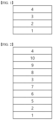
- FIG. 1 shows an example of an organic light emitting device comprising a substrate 1, an anode 2, a light emitting layer 3, and a cathode 4.
- FIG. 2 shows an example of an organic light emitting device comprising a substrate 1, an anode 2, a hole injection layer 5, a hole transport layer 6, an electron blocking layer 7, a light emitting layer 3, a hole blocking layer 8, an electron transport layer 9, an electron injection layer 10, and a cathode 4.
- the organic light emitting device can be manufactured by sequentially stacking the above-described structures.
- the organic light emitting device may be manufactured by depositing a metal, metal oxides having conductivity, or an alloy thereof on the substrate by using a PVD (physical vapor deposition) method such as a sputtering method or an e-beam evaporation method to form the anode, forming the respective layers described above thereon, and then depositing a material that can be used as the cathode thereon.
- PVD physical vapor deposition
- the organic light emitting device can be manufactured by sequentially depositing from the cathode material to the anode material on a substrate in the reverse order of the above-mentioned configuration ( WO 2003/012890 ).
- the light emitting layer may be formed by subjecting hosts and dopants to a vacuum deposition method and a solution coating method.
- the solution coating method means a spin coating, a dip coating, a doctor blading, an inkjet printing, a screen printing, a spray method, a roll coating, or the like, but is not limited thereto.
- the organic light emitting device can be manufactured by sequentially depositing from the cathode material to the organic material layer and the anode material on a substrate ( WO 2003/012890 ).
- the organic light emitting device may be a bottom emission device, a top emission device, or a double-sided light emitting device, and particularly, may be a bottom emission device that requires relatively high luminous efficiency.
- Compound 2-3 was prepared in the same manner as in the preparation method of Compound 2-2, except that in Preparation Example 2-2, 5,8-dihydroindolo[2,3-c]carbazole was changed to 5,8-dihydroindolo[2,3-c]carbazole-1,2,4,6,7,9,11,12-d8, 4-bromo-1,1'-biphenyl-2,2',3,3',4',5,5',6,6'-d9 was changed to 3-bromo-1,1'-biphenyl, and 4-bromo-1,1':3',1"-terphenyl was changed to 3-bromodibenzo[b,d]furan-1,2,4,6,8,9-d6.
- MS: [M+H]+ 590
- Example 1 Manufacture of organic light emitting device
- a glass substrate on which a thin film of ITO (indium tin oxide) was coated in a thickness of 1400 ⁇ was put into distilled water containing the detergent dissolved therein and washed by ultrasonic wave.
- the used detergent was a product commercially available from Fisher Co. and the distilled water was one which had been twice filtered by using a filter commercially available from Millipore Co.
- the ITO was cleaned for 30 minutes, and ultrasonic cleaning was then repeated twice for 10 minutes by using distilled water. After the cleaning with distilled water was completed, the substrate was ultrasonically washed with the solvents of isopropyl alcohol, acetone, and methanol, and dried, after which it was transported to a plasma cleaner. Then, the substrate was cleaned with oxygen plasma for 5 minutes, and then transferred to a vacuum evaporator.
- the following Compound ET-A was vacuum-deposited to a thickness of 50 ⁇ as a hole blocking layer.
- the following Compound ET-B and Compound Liq were thermally vacuum-deposited at a weight ratio of 1:1 to a thickness of 300 ⁇ as an electron transport layer, and then, Yb (ytterbium) was vacuum-deposited to a thickness of 10 ⁇ as an electron injection layer.
- Magnesium and silver were deposited in a weight ratio of 1: 4 to a thickness of 150 ⁇ on the electron injection layer to form a cathode, thereby completing the manufacture of an organic light emitting device.
- the vapor deposition rate of the organic material was maintained at 0.4 ⁇ 0.7 ⁇ /sec, the deposition rate of magnesium and silver was maintained at 2 ⁇ /sec, and the degree of vacuum during the deposition was maintained at 2 ⁇ 10 -7 ⁇ 5 ⁇ 10 -6 torr, thereby manufacturing an organic light emitting device.
- the organic light emitting devices manufactured in Examples 1 to 10 and Comparative Examples 1 to 3 were heat-treated in an oven at 120°C for 30 minutes, then taken out, and the voltage, efficiency, and lifetime (T95) were measured by applying a current, and the results are shown in Table 1 below.
- T95 means the time (hr) required for the luminance to be reduced to 95% of the initial luminance at a current density of 20 mA/cm 2 .
- substrate 2 anode 3: light emitting layer 4: cathode 5: hole injection layer 6: hole transport layer 7: electron blocking layer 8: hole blocking layer 9: electron transport layer 10: electron injection layer
Landscapes
- Chemical & Material Sciences (AREA)
- Physics & Mathematics (AREA)
- Engineering & Computer Science (AREA)
- Materials Engineering (AREA)
- Spectroscopy & Molecular Physics (AREA)
- Optics & Photonics (AREA)
- Organic Chemistry (AREA)
- Electroluminescent Light Sources (AREA)
Applications Claiming Priority (2)
| Application Number | Priority Date | Filing Date | Title |
|---|---|---|---|
| KR20220011716 | 2022-01-26 | ||
| PCT/KR2023/001224 WO2023146319A1 (ko) | 2022-01-26 | 2023-01-26 | 유기 발광 소자 |
Publications (2)
| Publication Number | Publication Date |
|---|---|
| EP4401536A1 true EP4401536A1 (de) | 2024-07-17 |
| EP4401536A4 EP4401536A4 (de) | 2025-01-01 |
Family
ID=87471995
Family Applications (1)
| Application Number | Title | Priority Date | Filing Date |
|---|---|---|---|
| EP23747360.8A Pending EP4401536A4 (de) | 2022-01-26 | 2023-01-26 | Organische lichtemittierende vorrichtung |
Country Status (5)
| Country | Link |
|---|---|
| US (1) | US20240397737A1 (de) |
| EP (1) | EP4401536A4 (de) |
| KR (1) | KR102825902B1 (de) |
| CN (1) | CN118020405A (de) |
| WO (1) | WO2023146319A1 (de) |
Families Citing this family (3)
| Publication number | Priority date | Publication date | Assignee | Title |
|---|---|---|---|---|
| JP2024007687A (ja) * | 2022-07-06 | 2024-01-19 | 株式会社Kyulux | 新規な材料を使用する有機発光素子、および有機発光素子の寿命の延長方法 |
| KR20250098454A (ko) * | 2023-12-22 | 2025-07-01 | 엘티소재주식회사 | 헤테로고리 화합물, 유기 발광 소자 및 유기 발광 소자의 유기물층용 조성물 |
| US20260090194A1 (en) | 2024-09-23 | 2026-03-26 | Dupont Specialty Materials Korea Ltd. | Organic electroluminescent device |
Family Cites Families (9)
| Publication number | Priority date | Publication date | Assignee | Title |
|---|---|---|---|---|
| KR100430549B1 (ko) | 1999-01-27 | 2004-05-10 | 주식회사 엘지화학 | 신규한 착물 및 그의 제조 방법과 이를 이용한 유기 발광 소자 및 그의 제조 방법 |
| DE10135513B4 (de) | 2001-07-20 | 2005-02-24 | Novaled Gmbh | Lichtemittierendes Bauelement mit organischen Schichten |
| KR101929448B1 (ko) * | 2016-07-20 | 2018-12-14 | 주식회사 엘지화학 | 신규한 화합물 및 이를 포함하는 유기발광 소자 |
| KR20190079341A (ko) * | 2017-12-27 | 2019-07-05 | 삼성에스디아이 주식회사 | 유기 화합물, 조성물, 유기 광전자 소자 및 표시 장치 |
| KR102447008B1 (ko) * | 2019-08-09 | 2022-09-22 | 주식회사 엘지화학 | 유기 발광 소자 |
| WO2021029616A1 (ko) * | 2019-08-09 | 2021-02-18 | 주식회사 엘지화학 | 유기 발광 소자 |
| KR102275039B1 (ko) * | 2019-10-08 | 2021-07-08 | 엘티소재주식회사 | 유기 발광 소자, 이의 제조 방법 및 유기 발광 소자의 유기물층용 조성물 |
| CN115244723A (zh) * | 2020-03-11 | 2022-10-25 | 默克专利有限公司 | 有机电致发光器件 |
| EP4163988A4 (de) * | 2020-07-15 | 2024-01-24 | Lg Chem, Ltd. | Organisches lichtemittierendes element |
-
2023
- 2023-01-26 EP EP23747360.8A patent/EP4401536A4/de active Pending
- 2023-01-26 US US18/693,515 patent/US20240397737A1/en active Pending
- 2023-01-26 KR KR1020230010452A patent/KR102825902B1/ko active Active
- 2023-01-26 WO PCT/KR2023/001224 patent/WO2023146319A1/ko not_active Ceased
- 2023-01-26 CN CN202380013796.1A patent/CN118020405A/zh active Pending
Also Published As
| Publication number | Publication date |
|---|---|
| EP4401536A4 (de) | 2025-01-01 |
| KR20230115267A (ko) | 2023-08-02 |
| CN118020405A (zh) | 2024-05-10 |
| WO2023146319A1 (ko) | 2023-08-03 |
| KR102825902B1 (ko) | 2025-06-26 |
| US20240397737A1 (en) | 2024-11-28 |
Similar Documents
| Publication | Publication Date | Title |
|---|---|---|
| EP3862355A1 (de) | Neuartige verbindung und organische lichtemittierende vorrichtung damit | |
| EP3982434B1 (de) | Organische lichtemittierende vorrichtung | |
| EP4400501B1 (de) | Neuartige verbindung und organische lichtemittierende vorrichtung damit | |
| EP3862350B1 (de) | Neuartige verbindung und organische lichtemittierende vorrichtung mit verwendung davon | |
| EP4243102A1 (de) | Organische lichtemittierende vorrichtung | |
| EP3961736A1 (de) | Organische lichtemittierende vorrichtung | |
| EP4254528A1 (de) | Organische lichtemittierende vorrichtung | |
| EP4401536A1 (de) | Organische lichtemittierende vorrichtung | |
| EP4266390B1 (de) | Organische lichtemittierende vorrichtung | |
| EP3539953A1 (de) | Neuartige verbindung und organische lichtemittierende vorrichtung mit verwendung davon | |
| EP3730488B1 (de) | Neuartige heterocyclische verbindung und organische lichtemittierende vorrichtung mit verwendung davon | |
| KR20260008209A (ko) | 유기 발광 소자 | |
| EP4357341A1 (de) | Neuartige verbindung und organische lichtemittierende vorrichtung damit | |
| EP4289836A1 (de) | Neuartige verbindung und organische lichtemittierende vorrichtung damit | |
| EP4270509A1 (de) | Organische lichtemittierende vorrichtung | |
| EP4270508A1 (de) | Organische lichtemittierende vorrichtung | |
| EP4486098A1 (de) | Organische lichtemittierende vorrichtung | |
| EP4335845A1 (de) | Neuartige verbindung und organische lichtemittierende vorrichtung damit | |
| EP4261906A1 (de) | Organische lichtemittierende vorrichtung | |
| KR20240122330A (ko) | 신규한 화합물 및 이를 이용한 유기 발광 소자 | |
| KR102576736B1 (ko) | 유기 발광 소자 | |
| KR20210008814A (ko) | 신규한 화합물 및 이를 이용한 유기 발광 소자 | |
| EP4299574B1 (de) | Neuartige verbindung und organische lichtemittierende vorrichtung damit | |
| EP4242205B1 (de) | Neuartige verbindung und organische lichtemittierende vorrichtung damit | |
| EP4345099A1 (de) | Neuartige verbindung und organische lichtemittierende vorrichtung damit |
Legal Events
| Date | Code | Title | Description |
|---|---|---|---|
| STAA | Information on the status of an ep patent application or granted ep patent |
Free format text: STATUS: THE INTERNATIONAL PUBLICATION HAS BEEN MADE |
|
| PUAI | Public reference made under article 153(3) epc to a published international application that has entered the european phase |
Free format text: ORIGINAL CODE: 0009012 |
|
| STAA | Information on the status of an ep patent application or granted ep patent |
Free format text: STATUS: REQUEST FOR EXAMINATION WAS MADE |
|
| 17P | Request for examination filed |
Effective date: 20240408 |
|
| AK | Designated contracting states |
Kind code of ref document: A1 Designated state(s): AL AT BE BG CH CY CZ DE DK EE ES FI FR GB GR HR HU IE IS IT LI LT LU LV MC ME MK MT NL NO PL PT RO RS SE SI SK SM TR |
|
| A4 | Supplementary search report drawn up and despatched |
Effective date: 20241204 |
|
| RIC1 | Information provided on ipc code assigned before grant |
Ipc: H10K 101/10 20230101ALN20241128BHEP Ipc: H10K 101/00 20230101ALN20241128BHEP Ipc: H10K 50/00 20230101ALI20241128BHEP Ipc: C09K 11/06 20060101ALI20241128BHEP Ipc: H10K 50/11 20230101ALI20241128BHEP Ipc: H10K 85/60 20230101AFI20241128BHEP |
|
| DAV | Request for validation of the european patent (deleted) | ||
| DAX | Request for extension of the european patent (deleted) | ||
| STAA | Information on the status of an ep patent application or granted ep patent |
Free format text: STATUS: EXAMINATION IS IN PROGRESS |
|
| 17Q | First examination report despatched |
Effective date: 20251113 |