EP4404101A2 - Support de données sous forme de carte, produit semi-fini et disposition de contacts pour celui-ci, et procédé pour sa fabrication - Google Patents
Support de données sous forme de carte, produit semi-fini et disposition de contacts pour celui-ci, et procédé pour sa fabrication Download PDFInfo
- Publication number
- EP4404101A2 EP4404101A2 EP24180889.8A EP24180889A EP4404101A2 EP 4404101 A2 EP4404101 A2 EP 4404101A2 EP 24180889 A EP24180889 A EP 24180889A EP 4404101 A2 EP4404101 A2 EP 4404101A2
- Authority
- EP
- European Patent Office
- Prior art keywords
- contact
- electronic component
- contact pads
- electrically conductive
- card
- Prior art date
- Legal status (The legal status is an assumption and is not a legal conclusion. Google has not performed a legal analysis and makes no representation as to the accuracy of the status listed.)
- Pending
Links
Images

Classifications
-
- G—PHYSICS
- G06—COMPUTING OR CALCULATING; COUNTING
- G06K—GRAPHICAL DATA READING; PRESENTATION OF DATA; RECORD CARRIERS; HANDLING RECORD CARRIERS
- G06K19/00—Record carriers for use with machines and with at least a part designed to carry digital markings
- G06K19/06—Record carriers for use with machines and with at least a part designed to carry digital markings characterised by the kind of the digital marking, e.g. shape, nature, code
- G06K19/067—Record carriers with conductive marks, printed circuits or semiconductor circuit elements, e.g. credit or identity cards also with resonating or responding marks without active components
- G06K19/07—Record carriers with conductive marks, printed circuits or semiconductor circuit elements, e.g. credit or identity cards also with resonating or responding marks without active components with integrated circuit chips
- G06K19/072—Record carriers with conductive marks, printed circuits or semiconductor circuit elements, e.g. credit or identity cards also with resonating or responding marks without active components with integrated circuit chips the record carrier comprising a plurality of integrated circuit chips
-
- G—PHYSICS
- G06—COMPUTING OR CALCULATING; COUNTING
- G06K—GRAPHICAL DATA READING; PRESENTATION OF DATA; RECORD CARRIERS; HANDLING RECORD CARRIERS
- G06K19/00—Record carriers for use with machines and with at least a part designed to carry digital markings
- G06K19/06—Record carriers for use with machines and with at least a part designed to carry digital markings characterised by the kind of the digital marking, e.g. shape, nature, code
- G06K19/067—Record carriers with conductive marks, printed circuits or semiconductor circuit elements, e.g. credit or identity cards also with resonating or responding marks without active components
- G06K19/07—Record carriers with conductive marks, printed circuits or semiconductor circuit elements, e.g. credit or identity cards also with resonating or responding marks without active components with integrated circuit chips
- G06K19/0716—Record carriers with conductive marks, printed circuits or semiconductor circuit elements, e.g. credit or identity cards also with resonating or responding marks without active components with integrated circuit chips at least one of the integrated circuit chips comprising a sensor or an interface to a sensor
- G06K19/0718—Record carriers with conductive marks, printed circuits or semiconductor circuit elements, e.g. credit or identity cards also with resonating or responding marks without active components with integrated circuit chips at least one of the integrated circuit chips comprising a sensor or an interface to a sensor the sensor being of the biometric kind, e.g. fingerprint sensors
-
- G—PHYSICS
- G06—COMPUTING OR CALCULATING; COUNTING
- G06K—GRAPHICAL DATA READING; PRESENTATION OF DATA; RECORD CARRIERS; HANDLING RECORD CARRIERS
- G06K19/00—Record carriers for use with machines and with at least a part designed to carry digital markings
- G06K19/06—Record carriers for use with machines and with at least a part designed to carry digital markings characterised by the kind of the digital marking, e.g. shape, nature, code
- G06K19/067—Record carriers with conductive marks, printed circuits or semiconductor circuit elements, e.g. credit or identity cards also with resonating or responding marks without active components
- G06K19/07—Record carriers with conductive marks, printed circuits or semiconductor circuit elements, e.g. credit or identity cards also with resonating or responding marks without active components with integrated circuit chips
- G06K19/077—Constructional details, e.g. mounting of circuits in the carrier
- G06K19/0772—Physical layout of the record carrier
Definitions
- the invention relates generally to the field of card-shaped electronic data carriers, in particular chip cards, such as credit and debit cards, and in particular to such data carriers which have two electronic components which are arranged separately in the data carrier but are electrically connected to one another.
- the invention relates to the data carriers as such as well as semi-finished products and contact layouts therefor, and methods for their production.
- the antenna device is laid, for example, as a coil on a layer inside the card, in the so-called card inlay, and has two contact pads that are electrically connected to two corresponding contact surfaces on the underside of a chip module containing the chip.
- the card inlay is laminated with one or more further layers so that the surface of the card inlay that carries the antenna device is inside the card. A cavity is then milled into the card body, into which the chip module is inserted.
- a silicone compound with metallic particles can serve as a connection between the contact pads of the antenna coil and the contact surfaces of the chip module above it. This compound remains elastic after curing and thus forms a reliable connection with the contact surfaces of the chip module placed on top of the silicone compound (so-called flex bump technology).
- an electrically conductive solder paste is applied to the respective contact pad of the antenna device and liquefied in a local melting process so that it creates a reliable electrically conductive connection to the contact surfaces of the chip module, which becomes permanent when the solder cools down (so-called TeConnect method).
- the contact pads of the antenna device are provided with an anisotropically conductive film (ACF). This is a hot-melt plastic material with conductive particles distributed in it, which only conducts electrically perpendicular to the contact pad, so that the film can be applied over a relatively large area, even across several contact pads, without electrically short-circuiting these contact pads (so-called ACF connection technology).
- an electronic card-shaped data carrier can have other electronic components, in particular sensors such as a fingerprint sensor. Such sensors can be used to identify an authorized user and to activate the cards. Like the antenna coil, they must be electrically connected to the chip of the chip card in order to be able to communicate with the chip. This can be done in the same way as previously explained with regard to the antenna device.
- One or more first contact pads of the card inlay for contacting a first electronic component must therefore be electrically connected to one or more second contact pads for contacting a second electronic component.
- the contact pads and the electrically conductive connections between the contact pads are made using one and the same wire to reduce the manufacturing effort, by laying the wire in the area of the contact pads in a meandering or zigzag shape on the card inlay so that the contact pad is sufficiently densely covered with the wire so that contact can be reliably made from above.
- the wire is laid with the help of ultrasound so that it digs into the surface of the card inlay and does not affect the thickness of the card body.
- the wire itself is usually plastic-coated, with the plastic coating in the area of the contact pads being removed during milling.
- the EP 3 159 832 A1 describes an authentication token comprising an authentication module and at least one conductive wire for operatively connecting the authentication module to at least one further module of the token, wherein the at least one conductive wire is embedded in a non-conductive substrate of the token.
- the object of the present invention is therefore to provide a solution in this context as to how, in a card-shaped data carrier with several electronic components that are electrically conductively connected to one another, two contact surfaces of one of these two components and a contact pad of the other component can be electrically conductively connected to one another in a reliable manner.
- a contact layout of a corresponding multilayer card-shaped data carrier can have a first contact pad for connecting a first electronic component and preferably at least two second contact pads for connecting a second electronic component as well as electrically conductive connections on the one hand between the first contact pad and a first of the second contact pads and on the other hand between the first of the second contact pads and a second of the second contact pads.
- the contact pads mentioned are each formed by a meandering wire and are also referred to below as wire pads.
- a continuous wire is used for this purpose, which forms both the contact pads mentioned and the electrically conductive connection.
- This wire is laid in the first of the second contact surfaces as a double meander, namely preferably in such a way that a first part of the wire forms first meander loops lined up in a first direction and an adjoining second part of the continuous wire forms second meander loops lined up in an opposite direction, the first and second meander loops being nested in one another.
- the interlocking forward and backward guidance of the wire laid in a double meander form forms an "interdigital structure".
- a wire path in the wire pad is possible in such a way that the end of the wire running into the contact pad and the end of the wire leading out of the contact pad are at the same end of the contact pad. If the contact pad is then arranged in the card body in such a way that the corresponding opposite end of the contact pad faces the cavity to be milled out, the electrical connection between the first and the second contact pad is not damaged if the double meander-shaped contact pad is milled when the cavity is milled out.
- the contact pads for connecting the first and second electronic components as well as the electrically conductive connections between the contact pads are formed by two continuous wires.
- the first continuous wire forms the (at least one) first contact pad for the first electronic component and the first of the (at least two) two contact pads for the second electronic component as well as a connecting line between these two contact pads.
- the second wire forms the second of the second contact pads and a connecting line leading out of it.
- an electrically conductive connecting element is provided which connects the connecting line formed by the first wire and the second wire is "superimposed" on the connecting line formed by the second wire and is connected to one another in an electrically conductive manner.
- the electrically conductive connecting element can cover the area of the connecting line of the first continuous wire and the area of the connecting line of the second continuous wire from above.
- the electrically conductive connecting element can be provided first on the card inlay and both the laying of the first continuous wire in the area of the connecting line and the laying of the second continuous wire in the area of the connecting line can be carried out over the electrically conductive connecting element, so that the electrically conductive connecting element lies under the continuous wire and the connecting line.
- the electrically conductive connecting element is preferably metallic, in particular copper, and the electrically conductive connection between the electrically conductive connecting element and the connecting line of the first continuous wire on the one hand and between the electrically conductive connecting element and the connecting line of the second continuous wire on the other hand is a welded connection.
- the welded connection is in turn preferably a thermocompression welded connection in which metal is welded to metal by welding the metallic electrically conductive connecting element to the respective wire.
- the thermocompression welding is in turn preferably carried out with the assistance of ultrasound. In the process, both any plastic coating of the wires and any oxide layer of the metallic electrically conductive connecting element are rubbed away before the elements are finally welded together.
- the region of the connecting line of the first continuous wire and the region of the connecting line of the second continuous wire, which are to be connected to one another by means of the electrically conductive connecting element are so close to one another that the electrically conductive connection between the connecting element and the connecting line on the one hand and between the connecting element and the connecting line on the other hand is a common connection point can be formed, in particular as a continuous welded connection, which can advantageously be produced in a single process step, e.g. by thermocompression welding.
- the connecting element is preferably a thin copper element or another electrically conductive element, particularly preferably a metallized film, e.g. a PVC film or another suitable plastic film.
- a third aspect of the present disclosure also provides that the contact pads and the electrically conductive connections therebetween are created by means of two continuous wires.
- the first continuous wire forms the (at least one) first contact pad for the first electronic component and the first of the (at least two) second contact pads for the second electronic component as well as a connecting line between these two contact pads.
- the second wire forms the second of the second contact pads and a connecting line leading out of it.
- the electrically conductive connection is not created by means of an additional electrically conductive connecting element, but instead the first continuous wire forms an additional meandering contact pad in a region of its connecting line, and this additional meandering contact pad overlaps with the connecting line formed by the second wire.
- the electrically conductive connection between the second wire and the first wire in the region of the additional meander-shaped contact pad is again preferably a thermo-compression weld connection in which the wires are welded directly to one another, if necessary again with the assistance of ultrasound.
- the additional contact pad is preferably shifted towards the adjacent contact pad for the second electronic component or towards the adjacent contact pad for the first electronic component, so that these two contact pads together form a large contact pad, which is preferably at least 50% larger than a normal contact pad, in particular than the other contact pad for the second electronic component or than another or all other contact pads for the first electronic component.
- a large contact pad which is preferably at least 50% larger than a normal contact pad, in particular than the other contact pad for the second electronic component or than another or all other contact pads for the first electronic component.
- the additional wire pad can be dispensed with and the connecting line can be directly superimposed on the first of the second contact pads or on the at least one first contact pad, and the electrically conductive connection can be made in the superimposition area.
- Component is formed by an electrically conductive solder material, which preferably connects these two contact pads in a direct line.
- two contact pads for the second electronic component are not electrically connected to one another, but instead two contact surfaces of the electronic component itself are electrically connected.
- the contact layout on the card inlay again comprises a first contact pad for connecting a first electronic component and at least one second contact pad for connecting a second electronic component, as well as an electrically conductive connection between the first contact pad and the second contact pad.
- the contact pads mentioned are preferably each formed by a meandering wire.
- the second electronic component has at least two contact surfaces that are to be short-circuited.
- an electrically conductive connection is provided between the two contact surfaces of the second electronic component by means of an electrically conductive material that is applied to the two contact surfaces and connects them directly to one another. The electrical connection is therefore prefabricated on the electronic component in question before it is inserted into the card body, and is not created on the card inlay.
- This fifth aspect of the present disclosure is particularly suitable for the production of cards in which the contact between the contact pads on the card inlay and the associated contact surfaces of the electronic components is made by means of an anisotropically conductive film (ACF connection technology).
- the electrically conductive material that directly connects the two contact surfaces of the second electronic component is preferably a wire, preferably uninsulated, or alternatively a line of isotropic conductive paste, which may have to harden, or a line of an isotropically conductive plastic.
- the latter alternatives have the advantage that they have less of an impact on the thickness of the card body to be produced.
- the result is in any case a semi-finished product which comprises the contact layout and at least the second electronic component, which are preferably electrically connected to one another by means of an ACF film.
- the contact layout or the surface of the plastic layer on which the contact layout is prepared is ultimately located as a card inlay inside the final multilayer card-shaped data carrier.
- the card inlay layer is laminated with further layers, namely at least one artwork layer covering the contact layout, which is printed with a design and information or provided in another way, and, if the back of the card inlay layer is provided with a similar design or information, preferably a corresponding artwork layer on the back of the card inlay layer.
- a transparent protective layer can be provided on top of each, either as a transparent film or as a transparent protective varnish, in order to form the multilayer card body for the card-shaped data carrier, in which the contact layout and the electronic components electrically connected to one another are integrated.
- a corresponding plurality of areas of a multi-use sheet for example a PVC film
- a suitable metal in particular copper
- a corresponding multi-use sheet namely at least one such metallically coated area per card of the multi-use sheet.
- card-shaped data carriers in particular multilayer card-shaped data carriers, with at least two electronic components, for example a chip card with a conventional chip and one or more electronic components, such as a fingerprint sensor or an iris sensor or other sensors for authenticating a card user.
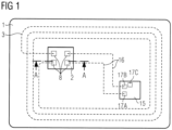
- the Figure 1 such a data carrier schematically in plan view.
- the card body 1 of this chip card contains a coil element 3, which serves as a transmitting and receiving antenna for an integrated circuit of a chip module 2 (not shown in the figure).
- the coil element 3 is in the Figure 1 In the embodiment shown, the coil element 3 is completely embedded in the card body.
- the coil element 3 is Figure 1 shown schematically by a dashed line.
- the chip module 2 is inserted in a recess of the card body and is electrically connected to the coil element 3 via contact surfaces 8 provided on the underside of the chip module 2.
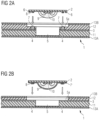
- FIG. 2A shows the Figure 1 shown chip card in a sectional view when inserting the chip module 2 into a two-stage cavity 5 of the card body 1.
- the section was taken along the Figure 1 drawn line AB.
- the card body 1 is multi-layered and comprises at least one card inlay 11 with the coil element 3 arranged thereon including contact pads 4, a cover layer 12, which can be designed as an artwork layer and is accordingly printed on its top side, for example, and optionally transparent protective layers 13A, 13B, which here form the outer layers of the card body.
- the protective layers 13A, 13B can be provided as a lacquer layer or as a film.
- the inlay layer 11 can be on the back just like the cover layer 12 as
- Artwork layer or an additional artwork layer can be provided between the inlay layer 11 and the lower protective layer 13A.
- the film layers 11 and 12 can in turn consist of several individual film layers.
- a two-stage recess 5 with a shoulder area 5a is milled into the card body 1, into which the chip module 2 is inserted from above.
- the chip module 2 is typically fitted into the recess 5 within the applicable technical tolerances so that the surface of the chip module 2 is flush with the surface of the card body 1 and the contact surfaces 8 on the underside of the chip module 2 lie opposite the contact pads 4 of the coil element 3, which have been exposed by milling and partially removed in the process.
- the recess 5 is dimensioned such that it can accommodate the chip module 2 together with a potting compound 9 that surrounds an integrated circuit 10.
- the mechanical connection between the chip module 2 and the card body 1 can be produced, for example, using a thermally activated adhesive 6.
- the electrical connection between the chip module 2 and the coil element 3 contained in the card body 1 can be made by means of a conductive elastomer 7 (e.g. Flex-Bump from Mühlbauer), which is applied to the contact pads 4 of the coil element 3 or, as here, typically to the contact surfaces 8 of the chip module 2.
- a conductive elastomer 7 e.g. Flex-Bump from Mühlbauer
- the conductive elastomer is preferably a silicone mass with metallic particles, which remains elastic after curing and thus forms a reliable electrically conductive connection with the contact surfaces 8 of the chip module 2 resting on the silicone mass from above (so-called flex bump technology).
- an electrically conductive solder paste can be applied to the respective contact pad 4 of the coil element 3 and liquefied in a local melting process so that the solder paste provides a reliable creates an electrically conductive connection to the contact surfaces 8 of the chip module 2, which becomes permanent when the solder cools down (TeConnect process).
- the contact pads 4 of the coil element 3 are provided with an anisotropically conductive foil 7 ⁇ (ACF foil).
- ACF foil anisotropically conductive foil 7 ⁇
- the corresponding card structure is shown in Figure 2B shown.
- the recess is milled down to the wire level 3.
- the ACF film 7 ⁇ is a hot-melt plastic material with conductive particles distributed within it, whereby the film only conducts electricity perpendicular to the contact pad 4, so that the film can be applied over a large area, even across several contact pads 4, without electrically short-circuiting these contact pads 4.
- the ACF film 7 ⁇ is typically applied flatly to the underside of the chip module.
- Figure 1 also shows a further contact surface 17C on the underside of the second electronic component 15, corresponding to the contact surfaces 8 of the chip module 2 in Figure 2A .
- the various aspects described below are concerned with establishing an electrically conductive connection between the contact surfaces 17B and 17C of the second electronic component 15.
- All of the embodiments described below have in common that the contact layout on the inlay layer 11 is formed by wires that are embedded in the surface of the inlay layer 11.
- the wire is laid on the inlay layer and subjected to ultrasound so that it digs into the surface due to the vibrations generated.
- Contact pads of the contact layout are created by laying the wire in a meandering or zigzag manner, and the electrically conductive connections 16 between the contact pads are also formed by the wire from which the pads were made.
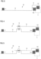
- FIG. 3 schematically shows a part of a contact layout 20 applied to the inlay layer 11 in plan view.
- This part of the contact layout 20 comprises two contact pads 4 and 14B, which are electrically connected by means of the connecting line 16 and are formed by a continuous wire, the wire running in a meandering manner in the area of the contact pads 4 and 14B.
- a third contact pad 14C is present, which is used to contact the in Figure 1 shown contact surface 17C of the second electronic component 15.
- the same wire with which the contact pads 4, 14B and the electrically conductive connection 16 are formed leads from the contact pad 14B to the contact pad 14C and is also laid in a meandering shape there in order to form the contact pad 14C.
- all contact pads 4, 14B, 14C and the connecting lines 16 are formed by a continuous wire.
- the special feature of this aspect of the present disclosure is that the wire is laid as a double meander in the area of the contact pad 14B and preferably leads out on the side of the contact pad 14B where the connecting line 16 leads into the contact pad 14B.
- the contact pads 14B and 14C are located in the shoulder area 5a of the Figure 2B It may happen when milling the two-stage recess, especially in the case of tolerance deviations in card production, that the deeper part of the two-stage recess 5, which is shown in Figure 3 indicated by a frame shown in dashed lines, mills away part of the contact pad 14B.
- the wire in the area of the contact pad 14B is severed and initially no longer leads to the other contact pad 14C.
- this contact pad 14B is subsequently connected to an associated contact surface 17B of the electronic component 15, for example by means of an electrically conductive adhesive or solder or via an electrically conductive ACF foil, then the nested meander loops of the wire laid as a double meander are short-circuited, so that an electrically conductive connection to the contact pad 14C is again established.
- the double meander is preferably laid such that a first part of the continuous wire forms first meander loops arranged in a first direction and an adjoining second part of the continuous wire forms second meander loops arranged in an opposite direction of travel, so that the first and second meander loops are nested in one another.
- the connections 16 to the contact pads 4 and 14C preferably enter the contact pad 14B at locations which are as far away from the recess 5 as possible, preferably on the side of the contact pad 14B facing away from the recess 5.
- the contact layout comprises a first contact pad 4 for connecting a first electronic component, for example the chip module 2, and at least two contact pads 14B, 14C for connecting the second electronic component 15, as well as an electrically conductive connection 16 between the first contact pad 4 and the first of the second contact pads 14B and a further electrically conductive connection 18, 19 between the contact pad 14B and the further contact pad 14C, wherein the contact pads are each formed by a meandering wire.
- the second contact pad 14C is formed by its own continuous wire, which forms a connection line 18 leading out of the contact pad 14C, but which does not lead directly to the first contact pad 14B.
- an electrically conductive connecting element 19 is provided such that it overlays and connects a region of the connecting line 16 between the contact pads 4 and 14B and a region of the connecting line 18.
- the connecting element 19 can be a metallic element or a metallized element, for example a piece of copper or a thin copper foil or a metallized plastic foil, for example a PVC foil, particularly preferably a plastic foil coated with copper. It is possible to first apply the connecting element 19 to the inlay layer 11 and then lay the respective continuous wires in the area of the connecting line 16 and connecting line 18 over it, or to first lay the wires and then place the connecting element 19 over the connecting line 16 and connecting line 18.
- the electrical connections between the electrically conductive connecting element 19 and the connecting line 16 and connecting line 18 are in Fig.4 indicated by two ellipses and are preferably carried out by means of thermocompression welding.
- thermocompression welding is preferably carried out with the assistance of ultrasound, whereby both a plastic coating of the wires and any oxide layer of the metallic electrically conductive connecting element 19 are rubbed away before the elements are finally welded together.
- the embodiments according to Figures 4 and 5 differ only insofar as the connecting line 16 and the connecting line 18 in the embodiment according to Figure 5 are so close together that a single weld (in Fig.5 indicated by only an ellipse) is sufficient to electrically connect both lines 16, 18 to the connecting element 19.
- a separate welded connection is created for the connection of the connecting element 19 with the connecting line 16 on the one hand and with the connecting line 18 on the other hand.
- the electrically conductive connecting elements 19 for a plurality of chip cards on a correspondingly large-format plastic film which forms the inlay layer 11, wherein the electrically conductive connecting elements are provided as a partially metallic coating at the corresponding locations where an electrically conductive connection between adjacent lines 16, 18 is to be established.
- a corresponding number of connecting elements are inserted into prepared cutouts of the full-format sheet, whereupon the wires are then laid.
- a third aspect of the present disclosure is explained below with reference to Figures 6A and 6B explained, which in turn schematically show a part of a contact layout 20 applied to the inlay layer 11 in plan view.
- the solution according to the third aspect is similar to that of the second aspect.
- a fourth wire pad 21 is provided in addition to the connection pads 4, 14B and 14C designed as wire pads, namely as a component of the connecting line 16.
- the connecting lines 16 and the associated wire pads 4, 21 and 14B are formed by means of a continuous wire.
- the connecting line 18 leading out of the connection pad 14C is laid above or below the fourth wire pad 21, depending on which of the two wires is laid first.
- the electrically conductive connection between the connecting line 18 and the fourth wire pad 21 is then made, preferably again by means of thermocompression welding. This is shown in Fig. 6A indicated with an ellipse.
- the advantage of this solution compared to the solution according to the second aspect described above is that no additional material in the sense of another separate element is required to create the connection between the two wires, so that the thickness of the inlay layer 11 with the contact layout 20 located thereon is not increased compared to the double meander solution explained at the beginning.
- Fig. 6B shows an alternative to the embodiment from Fig. 6A such that the additional fourth wire pad 21 is displaced towards the contact pad 14B and preferably forms an enlargement of the contact pad 14B.
- This enlargement is preferably at least 50% and can be as in the embodiment according to Fig. 6B shown is approximately 100%.
- the additional fourth wire pad 21 can be displaced towards the contact pad 4 and preferably form an enlargement of the contact pad 4, so that the contact pad 4 preferably at least 50% and in particular, for example, 100% larger than one or all of the other contact pads 4 for contacting the first electronic component or for contacting the chip module 2.
- Shifting the fourth wire pad 21 to the wire pad 14B or to the wire pad 4 offers the advantage of reducing its visibility on the surface of the finished chip card.
- the fourth wire pad 21 is omitted and the connecting line 18 of the contact pad 14C is laid directly above or below the contact pad 14B, or alternatively above or below the contact pad 4.
- the two wires are electrically connected to one another in the region of the contact pad 14B at approximately the same point at which an electrical connection is later made between the contact pad 14B and the contact connection 17B of the associated second electronic component 15.
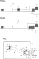
- FIG.7 schematically shows the data carrier 1 in plan view with a first electronic component inserted therein, here the chip module 2, and a second electronic component 15, which is still to be inserted into the two-stage recess 5 of the card body 1.
- the boxes 4 and 17A to 17C shown on the electronic components 2 and 15 represent connection surfaces of the respective electrical components, including the Fig.1 already mentioned connection surface 17C, which together with another connection surface 17B of the same electronic component 15 is to be electrically connected via a connecting line 16 to an associated connection surface 4 of the other electronic component 2.
- connecting lines 16 run inside the card body 1 on an inner surface of an inlay layer.
- the two-stage recess 5 including the shoulder area 5a is milled out of the card body 1, and local depressions are milled in the shoulder area 5a.
- the contact between the contact pads 14A, 14B, 14C on the one hand and the associated contact surfaces 17A, 17B, 17C of the second electronic component 15 on the other hand can be made, for example, in flex bump technology using a solder paste (e.g. TeConnect) or using ACF foil, as also previously explained.
- solder paste e.g. TeConnect
- ACF foil as also previously explained.
- the contact pads 14B and 14C are electrically connected to one another in such a way that the solder paste, or in the case of flex bump technology the electrically conductive plastic mass, is not only applied in the area of the contact pads 14B and 14C, but also that an electrically conductive connection 22 is thereby established directly between the two contact pads 14B and 14C.
- the shoulder region 5a of the second-stage recess 5 is not only milled away in the area of the contact pads 14B and 14C, but a connecting channel is also milled between them, in which the solder paste or the electrically conductive plastic is then laid along a continuous line in order to electrically connect the two contact pads 14B and 14C.
- the solder paste or the electrically conductive plastic is isotropic with respect to electrical conductivity.
- FIG. 8A A fifth aspect of the present disclosure is described below with reference to Figures 8A, 8B and 9 explained.
- the Figures 8A and 8B each schematically shows two embodiments of the second electronic component 15 in a top view. This can be inserted into the card body 1 in the same way as in relation to Fig.7 explained and in Fig.9
- the difference from the fourth aspect described above is that the additional contact pad 14C of the contact layout or the inlay layer can be dispensed with.
- the material for making the conductive connection between the two contact surfaces 17B and 17C of the electronic component 15 in Fig. 8A is a simple, preferably uninsulated wire 23.
- an isotropic conductive paste 24 is provided instead of the wire 23.
- Conductive paste refers to all materials that can be applied in any way to enable an electrical connection between two contact pads.
- This can be, for example, a solder or a paste filled with metallic particles of any shape, as well as carbon or other electrically conductive materials.
- the conductive paste hardens or dries before the electronic component 15 is inserted into the card body 1.
- On the card inlay only a one-to-one wire connection needs to be made between the respective contact pads 4 and 14A, 14B of the electronic components 2 and 15 to be connected to one another, which is preferably again formed by means of a continuous wire that runs in a meandering manner in the area of the contact pads.
- a contact layout for a multilayer card-shaped data carrier for example a chip card, can have at least one first contact pad for connecting a first electronic component and at least two second contact pads for connecting a second electronic component as well as electrically conductive connections on the one hand between the first contact pad and a first of the second contact pads and on the other hand between the first of the second contact pads and a second of the second contact pads, wherein the said contact pads are each formed by a meandering wire, wherein the contact layout can have a continuous wire which forms the said contact pads and the said electrically conductive connections and which is laid in the first of the second contact surfaces as a double meander, preferably in such a way that a first part of the continuous wire forms first meander loops arranged next to one another in a first direction and an adjoining second part of the continuous wire forms second meander loops arranged next to one another in an opposite direction of travel, wherein the first and second meander loops are nested within one another.
- a contact layout for a multilayer card-shaped data carrier for example a chip card, can have at least one first contact pad for connecting a first electronic component and at least two second contact pads for connecting a second electronic component as well as electrically conductive connections on the one hand between the first contact pad and a first of the second contact pads and on the other hand between the first of the second contact pads and a second of the second contact pads, wherein the said contact pads are each formed by a meandering wire, wherein the contact layout can have a first continuous wire which forms the at least one first contact pad and the first of the second contact pads as well as a connecting line between these two contact pads, and a second continuous wire which forms the second of the second contact pads as well as a connecting line leading out from it, wherein a An electrically conductive connecting element overlies a region of the connecting line of the first continuous wire and a region of the connecting line of the second continuous wire and connects them to one another in an electrically conductive manner.
- the electrically conductive connecting element can be metallic and the electrically conductive connection between the electrically conductive connecting element and the connecting line of the first continuous wire on the one hand and between the electrically conductive connecting element and the connecting line of the second continuous wire on the other hand can be a welded connection.
- the welded joint can be a thermo-compression welded joint.
- the region of the connecting line of the first continuous wire and the region of the connecting line of the second continuous wire can be so close to one another that the electrically conductive connection between the electrically conductive connecting element and the connecting line on the one hand and between the electrically conductive connecting element and the connecting line on the other hand is designed as a common connection point.
- the connecting element can be a copper element.
- the connecting element can be a metallized film, preferably a metallized PVC film.
- a contact layout for a multilayer card-shaped data carrier for example a chip card, can have at least one first contact pad for connecting a first electronic component and at least two second contact pads for connecting a second electronic component as well as electrically conductive connections on the one hand between the first contact pad and a first of the second contact pads and on the other hand between the first of the second contact pads and a second of the second contact pads, wherein the said contact pads are each formed by a meandering wire, wherein the contact layout has a first continuous wire which at least a first contact pad and the first of the second contact pads as well as a connecting line between these two contact pads, and a second continuous wire which forms the second of the second contact pads as well as a connecting line leading out therefrom, wherein the first continuous wire forms an additional meander-shaped contact pad in a region of the connecting line, and wherein the additional meander-shaped contact pad formed by the first continuous wire and the connecting line formed by the second continuous wire overlap one another and are electrically conductively connected to one another.
- the additional meander-shaped contact pad can form an enlargement of the first of the second contact pads or of the at least one first contact pad, so that the first of the second contact pads is larger than the second of the second contact pads or the at least one first contact pad is larger than another of the first contact pads.
- the first of the second contact pads can be at least 50% larger than the second of the second contact pads or the at least one first contact pad can be at least 50% larger than the other of the first contact pads.
- the enlargement of the first of the second contact pads formed by the additional meandering contact pad can extend in a direction away from a mounting location of the second electronic component.
- the electrically conductive connection of the connecting cable can be a thermo-compression welded connection with the additional meander-shaped contact pad.
- a contact layout for a multilayer card-shaped data carrier can comprise at least one first contact pad for connecting a first electronic component and at least two second contact pads for connecting a second electronic component, as well as electrically conductive connections on the one hand between the first contact pad and a first of the second contact pads and on the other hand between the first of the second contact pads and a second of the second contact pads, wherein the said contact pads are each formed by a meandering wire, wherein the contact layout can have a first continuous wire which forms the at least one first contact pad and the first of the second contact pads as well as a connecting line between these two contact pads, and a second continuous wire which forms the second of the second contact pads as well as a connecting line leading out therefrom, wherein either the at least one first contact pad or the first of the second contact pads on the one hand and the connecting line formed by the second continuous wire on the other hand overlap one another and are electrically conductively connected to one another.
- the electrically conductive connection of the connecting cable to the at least one first contact pad or the first of the second contact pads can be a thermo-compression welded connection.
- a contact layout for a multilayer card-shaped data carrier for example a chip card
- a semi-finished product for producing a multi-layer card-shaped data carrier can comprise a first electronic component and a second electronic component as well as a plastic layer with a surface which is intended to be and which comprises at least one contact layout, wherein the contact layout can comprise at least a first contact pad for connecting a first electronic component and at least one second contact pad for connecting a second electronic component as well as an electrically conductive connection between the first contact pad and the second contact pad, wherein said contact pads can preferably each be formed by a meandering wire and wherein the second electronic component can have at least two contact surfaces, wherein an electrically conductive connection between the two contact surfaces of the second electronic component is produced by means of an electrically conductive material which is applied to the two contact surfaces and connects them directly to one another.
- the electrically conductive material that directly connects the two contact surfaces of the second electronic component can be an uninsulated wire.
- the electrically conductive material that directly connects the two contact surfaces of the second electronic component can be a line of isotropic conductive paste.
- the semi-finished product can have at least one further second contact pad for connecting the second electronic component, wherein an anisotropically conductive film is provided on the at least two second contact pads for producing an electrically conductive connection with two corresponding contact surfaces of the second electronic component perpendicular to the second contact pads.
- a semi-finished product for producing a multilayer card-shaped data carrier for example a chip card
- the semi-finished product can be a multi-use sheet having several of the contact layouts.
- a multilayer card-shaped data carrier for example a chip card, can have a contact layout as described above or be made from a semi-finished product as described above.
- the data carrier can have at least one cover layer covering the contact layout with at least one recess for receiving the first or the second or both electronic components.
- the at least one recess may be a two-stage recess with a shoulder region extending over at least one of the contact pads of the contact layout.
- the data carrier can have a fingerprint sensor as one of the two electronic components and a microchip electrically connected to it.
- the connecting cable and the connection cable in the area of the electrically conductive connecting element can be laid so close to each other that the electrically conductive connection between the electrically conductive connecting element and the connecting cable on the one hand and between the electrically conductive connecting element and the connecting cable on the other hand is formed as a common connection point.
- the additional meander-shaped contact pad can be designed as an enlargement of the first of the second contact pads or of the at least one first contact pad, so that the first of the second contact pads is larger than the second of the second contact pads or the at least one first contact pad is larger than another of the first contact pads, wherein the first of the second contact pads is preferably 50% is formed larger than the second of the second contact pads or the at least one first contact pad is preferably formed at least 50% larger than the other of the first contact pads.
- the enlargement of the first of the second contact pads formed by the additional meandering contact pad can extend in a direction away from a mounting location of the second electronic component.
- the step of electrically conductive connection can be carried out by thermo-compression welding.
- the step of electrically conductive connection can be carried out by thermo-compression welding.
- the electrically conductive material that directly connects the two contact surfaces of the second electronic component can be an uninsulated wire.
- the electrically conductive material that directly connects the two contact surfaces of the second electronic component can be a line of isotropic conductive paste.
- At least one further second contact pad can be provided for connecting the second electronic component on the plastic substrate, and an anisotropically conductive film can be applied to the at least two second contact pads for producing an electrically conductive connection formed perpendicular to the second contact pads with two corresponding contact surfaces of the second electronic component.
- the plastic film can form a multi-use sheet on which a plurality of the first contact pads and the second contact pads are produced for a variety of contact layouts.
- an inner surface of a layer of the data carrier can be provided with a contact layout according to a method described above.
Landscapes
- Engineering & Computer Science (AREA)
- Computer Hardware Design (AREA)
- Microelectronics & Electronic Packaging (AREA)
- Physics & Mathematics (AREA)
- General Physics & Mathematics (AREA)
- Theoretical Computer Science (AREA)
- Automation & Control Theory (AREA)
- Credit Cards Or The Like (AREA)
Applications Claiming Priority (4)
| Application Number | Priority Date | Filing Date | Title |
|---|---|---|---|
| DE102021111570 | 2021-05-04 | ||
| DE102022109547.9A DE102022109547A1 (de) | 2021-05-04 | 2022-04-20 | Kartenförmiger Datenträger sowie Halbzeug und Kontaktlayout dafür, und Verfahren zur Herstellung derselben |
| PCT/EP2022/061403 WO2022233716A1 (fr) | 2021-05-04 | 2022-04-28 | Carte porteuse de données, produit semi-fini, agencement de câblage associé et procédé de production associé |
| EP22726424.9A EP4334841A1 (fr) | 2021-05-04 | 2022-04-28 | Carte porteuse de données, produit semi-fini, agencement de câblage associé et procédé de production associé |
Related Parent Applications (1)
| Application Number | Title | Priority Date | Filing Date |
|---|---|---|---|
| EP22726424.9A Division EP4334841A1 (fr) | 2021-05-04 | 2022-04-28 | Carte porteuse de données, produit semi-fini, agencement de câblage associé et procédé de production associé |
Publications (2)
| Publication Number | Publication Date |
|---|---|
| EP4404101A2 true EP4404101A2 (fr) | 2024-07-24 |
| EP4404101A3 EP4404101A3 (fr) | 2024-10-16 |
Family
ID=82404488
Family Applications (2)
| Application Number | Title | Priority Date | Filing Date |
|---|---|---|---|
| EP24180889.8A Pending EP4404101A3 (fr) | 2021-05-04 | 2022-04-28 | Support de données sous forme de carte, produit semi-fini et disposition de contacts pour celui-ci, et procédé pour sa fabrication |
| EP22726424.9A Pending EP4334841A1 (fr) | 2021-05-04 | 2022-04-28 | Carte porteuse de données, produit semi-fini, agencement de câblage associé et procédé de production associé |
Family Applications After (1)
| Application Number | Title | Priority Date | Filing Date |
|---|---|---|---|
| EP22726424.9A Pending EP4334841A1 (fr) | 2021-05-04 | 2022-04-28 | Carte porteuse de données, produit semi-fini, agencement de câblage associé et procédé de production associé |
Country Status (3)
| Country | Link |
|---|---|
| US (1) | US12361253B2 (fr) |
| EP (2) | EP4404101A3 (fr) |
| WO (1) | WO2022233716A1 (fr) |
Families Citing this family (3)
| Publication number | Priority date | Publication date | Assignee | Title |
|---|---|---|---|---|
| FR3128301B1 (fr) * | 2021-10-14 | 2024-06-14 | Smart Packaging Solutions | Carte à puce avec capteur biométrique |
| GB2618109A (en) * | 2022-04-27 | 2023-11-01 | Zwipe As | Smartcard milling technique |
| EP4510037A1 (fr) * | 2023-08-17 | 2025-02-19 | Thales Dis France Sas | Connexions d'inclusion de fil 1 à n |
Citations (1)
| Publication number | Priority date | Publication date | Assignee | Title |
|---|---|---|---|---|
| EP3159832A1 (fr) | 2015-10-23 | 2017-04-26 | Nxp B.V. | Jeton d'authentification |
Family Cites Families (4)
| Publication number | Priority date | Publication date | Assignee | Title |
|---|---|---|---|---|
| DE10258801A1 (de) | 2002-12-16 | 2004-07-22 | Siemens Ag | Verfahren und Vorrichtung zum Aufbringen eines pastenartigen Materials auf elektronische Bauelemente, Bestückvorrichtung |
| CN102629337A (zh) | 2012-04-12 | 2012-08-08 | 上海祯显电子科技有限公司 | 一种微型智能标签 |
| DE102012211546B4 (de) | 2012-07-03 | 2017-02-16 | Morpho Cards Gmbh | Chipkarte mit bei Raumtemperatur pastenförmiger oder flüssiger Kontaktierung |
| US10318852B2 (en) * | 2014-11-10 | 2019-06-11 | Golden Spring Internet Of Things Inc. | Smart card simultaneously having two read/write modes and method for producing same |
-
2022
- 2022-04-28 WO PCT/EP2022/061403 patent/WO2022233716A1/fr not_active Ceased
- 2022-04-28 EP EP24180889.8A patent/EP4404101A3/fr active Pending
- 2022-04-28 EP EP22726424.9A patent/EP4334841A1/fr active Pending
- 2022-04-28 US US18/559,121 patent/US12361253B2/en active Active
Patent Citations (1)
| Publication number | Priority date | Publication date | Assignee | Title |
|---|---|---|---|---|
| EP3159832A1 (fr) | 2015-10-23 | 2017-04-26 | Nxp B.V. | Jeton d'authentification |
Also Published As
| Publication number | Publication date |
|---|---|
| EP4334841A1 (fr) | 2024-03-13 |
| US12361253B2 (en) | 2025-07-15 |
| US20240242054A1 (en) | 2024-07-18 |
| EP4404101A3 (fr) | 2024-10-16 |
| WO2022233716A1 (fr) | 2022-11-10 |
Similar Documents
| Publication | Publication Date | Title |
|---|---|---|
| DE19534480C2 (de) | IC-Kartenmodul zur Herstellung einer IC-Karte sowie IC-Karte mit einem IC-Kartenmodul | |
| DE19710144C2 (de) | Verfahren zur Herstellung einer Chipkarte und nach dem Verfahren hergestellte Chipkarte | |
| EP0756244B1 (fr) | Unité électronique et procédé de fabrication de cette unité | |
| DE68921179T2 (de) | Elektronisches Modul mit einer integrierten Schaltung für ein kleines tragbares Objekt, z.B. eine Karte oder ein Schlüssel und Herstellungsverfahren für solche Module. | |
| EP1271399B1 (fr) | Porteur de données avec circuit intégré | |
| EP1162569B1 (fr) | Méthode de production d'un porteur de données | |
| EP4404101A2 (fr) | Support de données sous forme de carte, produit semi-fini et disposition de contacts pour celui-ci, et procédé pour sa fabrication | |
| DE3338597A1 (de) | Datentraeger mit integriertem schaltkreis und verfahren zur herstellung desselben | |
| DE112004001727T5 (de) | Verfahren zur Herstellung eines elektronischen Moduls | |
| DE10114355A1 (de) | Verfahren zur Herstellung einer kontaktlosen multifunktionalen Chipkarte sowie entsprechend hergestellte Chipkarte | |
| DE69905288T2 (de) | Verfahren zur herstellung einer kontaktlosen chipkarte | |
| EP2269168A1 (fr) | Carte à puce et son procédé de fabrication | |
| EP0976104A2 (fr) | Carte a puce, systeme de connexion et procede de production d'une carte a puce | |
| EP0757330A2 (fr) | Procédé de fabrication d'un support de données | |
| EP0996932A1 (fr) | Support de donnees exploitable sans contact | |
| DE19522338B4 (de) | Chipträgeranordnung mit einer Durchkontaktierung | |
| EP1527413A1 (fr) | Support de donnees avec solenoide de transpondeur | |
| WO2008138531A1 (fr) | Système de transmission sans contact et procédé de réalisation associé | |
| DE10324043B4 (de) | Kartenförmiger elektronischer Datenträger, Funktionsinlett dafür und ihre Herstellungsverfahren | |
| EP1374162B1 (fr) | Procede pour fabriquer un module | |
| DE102022109547A1 (de) | Kartenförmiger Datenträger sowie Halbzeug und Kontaktlayout dafür, und Verfahren zur Herstellung derselben | |
| DE10105069C2 (de) | Kopplungselement für Dual-Interface-Karte | |
| EP2239692B1 (fr) | Carte à puce et procédé destiné à sa fabrication | |
| DE19918852C1 (de) | Chipkarte mit Flip-Chip und Verfahren zu ihrer Herstellung | |
| WO1998048378A2 (fr) | Revetement pour cartes a puce |
Legal Events
| Date | Code | Title | Description |
|---|---|---|---|
| PUAI | Public reference made under article 153(3) epc to a published international application that has entered the european phase |
Free format text: ORIGINAL CODE: 0009012 |
|
| STAA | Information on the status of an ep patent application or granted ep patent |
Free format text: STATUS: REQUEST FOR EXAMINATION WAS MADE |
|
| 17P | Request for examination filed |
Effective date: 20240607 |
|
| AC | Divisional application: reference to earlier application |
Ref document number: 4334841 Country of ref document: EP Kind code of ref document: P |
|
| AK | Designated contracting states |
Kind code of ref document: A2 Designated state(s): AL AT BE BG CH CY CZ DE DK EE ES FI FR GB GR HR HU IE IS IT LI LT LU LV MC MK MT NL NO PL PT RO RS SE SI SK SM TR |
|
| REG | Reference to a national code |
Ref country code: DE Ref legal event code: R079 Free format text: PREVIOUS MAIN CLASS: G06K0019077000 Ipc: G06K0019070000 |
|
| PUAL | Search report despatched |
Free format text: ORIGINAL CODE: 0009013 |
|
| AK | Designated contracting states |
Kind code of ref document: A3 Designated state(s): AL AT BE BG CH CY CZ DE DK EE ES FI FR GB GR HR HU IE IS IT LI LT LU LV MC MK MT NL NO PL PT RO RS SE SI SK SM TR |
|
| RIC1 | Information provided on ipc code assigned before grant |
Ipc: G06K 19/077 20060101ALI20240910BHEP Ipc: G06K 19/07 20060101AFI20240910BHEP |
|
| STAA | Information on the status of an ep patent application or granted ep patent |
Free format text: STATUS: EXAMINATION IS IN PROGRESS |
|
| 17Q | First examination report despatched |
Effective date: 20250826 |