EP4411030A1 - Tranche monocristalline de carbure de silicium et lingot monocristallin de carbure de silicium - Google Patents
Tranche monocristalline de carbure de silicium et lingot monocristallin de carbure de silicium Download PDFInfo
- Publication number
- EP4411030A1 EP4411030A1 EP22876131.8A EP22876131A EP4411030A1 EP 4411030 A1 EP4411030 A1 EP 4411030A1 EP 22876131 A EP22876131 A EP 22876131A EP 4411030 A1 EP4411030 A1 EP 4411030A1
- Authority
- EP
- European Patent Office
- Prior art keywords
- silicon carbide
- crystal
- crystal silicon
- wafer
- carbide wafer
- Prior art date
- Legal status (The legal status is an assumption and is not a legal conclusion. Google has not performed a legal analysis and makes no representation as to the accuracy of the status listed.)
- Pending
Links
Images


Classifications
-
- C—CHEMISTRY; METALLURGY
- C30—CRYSTAL GROWTH
- C30B—SINGLE-CRYSTAL GROWTH; UNIDIRECTIONAL SOLIDIFICATION OF EUTECTIC MATERIAL OR UNIDIRECTIONAL DEMIXING OF EUTECTOID MATERIAL; REFINING BY ZONE-MELTING OF MATERIAL; PRODUCTION OF A HOMOGENEOUS POLYCRYSTALLINE MATERIAL WITH DEFINED STRUCTURE; SINGLE CRYSTALS OR HOMOGENEOUS POLYCRYSTALLINE MATERIAL WITH DEFINED STRUCTURE; AFTER-TREATMENT OF SINGLE CRYSTALS OR A HOMOGENEOUS POLYCRYSTALLINE MATERIAL WITH DEFINED STRUCTURE; APPARATUS THEREFOR
- C30B29/00—Single crystals or homogeneous polycrystalline material with defined structure characterised by the material or by their shape
- C30B29/10—Inorganic compounds or compositions
- C30B29/36—Carbides
-
- C—CHEMISTRY; METALLURGY
- C30—CRYSTAL GROWTH
- C30B—SINGLE-CRYSTAL GROWTH; UNIDIRECTIONAL SOLIDIFICATION OF EUTECTIC MATERIAL OR UNIDIRECTIONAL DEMIXING OF EUTECTOID MATERIAL; REFINING BY ZONE-MELTING OF MATERIAL; PRODUCTION OF A HOMOGENEOUS POLYCRYSTALLINE MATERIAL WITH DEFINED STRUCTURE; SINGLE CRYSTALS OR HOMOGENEOUS POLYCRYSTALLINE MATERIAL WITH DEFINED STRUCTURE; AFTER-TREATMENT OF SINGLE CRYSTALS OR A HOMOGENEOUS POLYCRYSTALLINE MATERIAL WITH DEFINED STRUCTURE; APPARATUS THEREFOR
- C30B19/00—Liquid-phase epitaxial-layer growth
- C30B19/02—Liquid-phase epitaxial-layer growth using molten solvents, e.g. flux
- C30B19/04—Liquid-phase epitaxial-layer growth using molten solvents, e.g. flux the solvent being a component of the crystal composition
-
- C—CHEMISTRY; METALLURGY
- C30—CRYSTAL GROWTH
- C30B—SINGLE-CRYSTAL GROWTH; UNIDIRECTIONAL SOLIDIFICATION OF EUTECTIC MATERIAL OR UNIDIRECTIONAL DEMIXING OF EUTECTOID MATERIAL; REFINING BY ZONE-MELTING OF MATERIAL; PRODUCTION OF A HOMOGENEOUS POLYCRYSTALLINE MATERIAL WITH DEFINED STRUCTURE; SINGLE CRYSTALS OR HOMOGENEOUS POLYCRYSTALLINE MATERIAL WITH DEFINED STRUCTURE; AFTER-TREATMENT OF SINGLE CRYSTALS OR A HOMOGENEOUS POLYCRYSTALLINE MATERIAL WITH DEFINED STRUCTURE; APPARATUS THEREFOR
- C30B19/00—Liquid-phase epitaxial-layer growth
- C30B19/10—Controlling or regulating
-
- C—CHEMISTRY; METALLURGY
- C30—CRYSTAL GROWTH
- C30B—SINGLE-CRYSTAL GROWTH; UNIDIRECTIONAL SOLIDIFICATION OF EUTECTIC MATERIAL OR UNIDIRECTIONAL DEMIXING OF EUTECTOID MATERIAL; REFINING BY ZONE-MELTING OF MATERIAL; PRODUCTION OF A HOMOGENEOUS POLYCRYSTALLINE MATERIAL WITH DEFINED STRUCTURE; SINGLE CRYSTALS OR HOMOGENEOUS POLYCRYSTALLINE MATERIAL WITH DEFINED STRUCTURE; AFTER-TREATMENT OF SINGLE CRYSTALS OR A HOMOGENEOUS POLYCRYSTALLINE MATERIAL WITH DEFINED STRUCTURE; APPARATUS THEREFOR
- C30B29/00—Single crystals or homogeneous polycrystalline material with defined structure characterised by the material or by their shape
- C30B29/60—Single crystals or homogeneous polycrystalline material with defined structure characterised by the material or by their shape characterised by shape
- C30B29/64—Flat crystals, e.g. plates, strips or discs
Definitions
- the present invention relates to a single-crystal silicon carbide wafer, and a single-crystal silicon carbide ingot.
- Patent Document 1 discloses a single-crystal silicon carbide obtained by a solution growth method. Furthermore, Patent Document 1 discloses a basal plane dislocation density and the like of the single-crystal silicon carbide.
- Patent Document 2 discloses a single-crystal silicon carbide obtained by a sublimation recrystallization method. Furthermore, Patent Document 2 discloses a basal plane dislocation density, a carrier concentration, and the like of the single-crystal silicon carbide.
- Patent Document 3 discloses a single-crystal silicon carbide obtained by a solution growth method. Furthermore, Patent Document 3 discloses a boron concentration, a nitrogen concentration, and the like of the single-crystal silicon carbide.
- Patent Document 4 discloses a single-crystal silicon carbide obtained by a sublimation recrystallization method. Furthermore, Patent Document 4 discloses a boron concentration, a nitrogen concentration, an aluminum concentration, a resistivity, and the like of the single-crystal silicon carbide.
- Patent Document 5 discloses a single-crystal silicon carbide obtained by a sublimation recrystallization method. Furthermore, Patent Document 5 discloses a boron concentration, a nitrogen concentration, an aluminum concentration, a resistivity, and the like of the single-crystal silicon carbide.
- Patent Document 6 discloses a single-crystal silicon carbide obtained by a sublimation recrystallization method. Furthermore, Patent Document 6 discloses a nitrogen concentration, an aluminum concentration, a specific resistance, a lamination defect density, and the like of the single-crystal silicon carbide.
- Patent Document 7 discloses a single-crystal silicon carbide obtained by a solution growth method.
- An object of the present invention is to realize a high-quality single-crystal silicon carbide that is not disclosed in Patent Documents 1 to 7.
- 4H-SiC or 6H-SiC represents a silicon carbide crystal having a crystal polymorph of 4H or 6H.
- H represents a hexagonal crystal, and the number represents the number of regular tetrahedron structural layers included in one period in a stacking direction.
- Fig. 1 shows an example of the single-crystal silicon carbide wafer 31 of the present embodiment.
- the single-crystal silicon carbide wafer 31 having a circular surface shape is shown in the figure.
- the single-crystal silicon carbide wafer 31 having a polygonal shape (hexagonal shape or the like) instead of the circular shape may be used. It is preferable that the single-crystal silicon carbide wafer 31 has a diameter of 100 mm or more and a thickness of 50 ⁇ m or more and 500 ⁇ m or less.
- the single-crystal silicon carbide wafer 31 is preferably cut from an ingot so that the surface is ⁇ 5 degrees or less from the (0001) surface of 4H-SiC or 6H-SiC, and the surface of the single-crystal silicon carbide wafer 31 may have an off angle that is inclined by 0.5 degrees or more and 5 degrees or less from the (0001) surface of the single-crystal silicon carbide.
- the single-crystal silicon carbide wafer 31 may have a flat portion called an orientation flat or a groove called a notch.
- the single-crystal silicon carbide wafer 31 has the following features 1 and 2. In addition, the single-crystal silicon carbide wafer 31 preferably has the following features 3 and 4.
- the single-crystal silicon carbide wafer 31 includes boron at a concentration of 1.0 ⁇ 10 16 atoms/cm 3 or less. Boron is included as an unavoidable impurity.
- Feature 1 is that the concentration of boron, which is an unavoidable impurity, is sufficiently reduced to 1.0 ⁇ 10 16 atoms/cm 3 or less.
- concentration range of boron which is an unavoidable impurity (the range of the concentration that can be mixed in the single-crystal silicon carbide wafer 31) is sufficiently narrowed down to more than 0 and 1.0 ⁇ 10 16 atoms/cm 3 or less.
- the range may be preferably more than 0 and 1.0 ⁇ 10 15 atoms/cm 3 or less.
- the concentration of boron which is an unavoidable impurity to be unintentionally added
- the characteristics for example, crystallinity and electrical characteristics
- the concentration of the impurity cannot be predicted or in a case the possible concentration range is wide where even though the prediction is possible, it becomes difficult to design products.
- the single-crystal silicon carbide wafer 31 with Feature 1 has a narrow concentration range of boron, which is an unavoidable impurity to be unintentionally added, of 1.0 ⁇ 10 16 atoms/cm 3 or less. Therefore, it becomes relatively easy to design products in consideration of the concentration of boron.
- the boron concentrations at all measurement points are 1.0 ⁇ 10 16 atoms/cm 3 or less, and an in-plane variation in the boron concentrations is small, it is considered that in-plane uniformity of the crystallinity or the electrical characteristics of the obtained single-crystal silicon carbide wafer 31 is good.
- the concentration of boron is a value measured at one point at the center of the single-crystal silicon carbide wafer 31 by secondary ion mass spectrometry (SIMS).
- SIMS secondary ion mass spectrometry
- a value measured in a dynamic SIMS mode using a secondary ion mass spectrometer (IMS 6f, CAMECA) was used.
- the variation in the boron concentration was evaluated based on the measurement results at one point at the center (hereinafter referred to as a "central point") of the single-crystal silicon carbide wafer 31 and four points in the periphery 50 mm apart from the center (hereinafter referred to as "peripheral points").
- the boron concentrations at these five points were measured by the same method as the measurement method for the one point at the center.
- an evaluation value is calculated by an expression of "(Boron concentration at peripheral point - Boron concentration at central point)/Boron concentration at central point", and in a case where an average value of the evaluation values of the four pairs is - 0.3 or more and 3.0 or less, and more preferably in a case where all of the evaluation values of the four pairs are -0.3 or more and 3.0 or less, the variation was defined to be small.
- the region is referred to as a "central region 33".
- the central region 33 includes the center of the surface of the single-crystal silicon carbide wafer 31 and is an undivided region. It is preferable that the center of the central region 33 and the center of the surface of the single-crystal silicon carbide wafer 31 overlap, and it is more preferable that the shape of the central region 33 and the shape of the surface of the single-crystal silicon carbide wafer 31 are the same as or similar to each other.
- the area of the central region 33 is one fourth or more of the area of the surface of the single-crystal silicon carbide wafer 31.
- the central region 33 may be preferably one third or more of the surface area.
- Feature 2 is that a central region 33 having a misorientation in a crystal plane sufficiently reduced to be as less as 50 arcsec or less is provided, and the central region 33 is as wide as one fourth or more of the surface area and includes the center of the surface.
- the central region 33 has excellent crystallinity by suppressing a strain in the crystal.
- the crystallinity is preferably 40 arcsec or less.
- the misorientation is an average value of the measurement results of the misorientation using an X-ray diffraction method at each of a total of five points of one point at the center of the single-crystal silicon carbide wafer 31 and four points in the outer peripheral part of the wafer (0 degrees, 90 degrees, 180 degrees, and 270 degrees, each of which is a point 80% of the wafer radius apart from the center).
- the measurement was performed using an X-ray diffractometer (SmartLab manufactured by Rigaku Corporation).
- the electrical resistivity of the single-crystal silicon carbide wafer 31 is 60 m ⁇ cm or less.
- Feature 3 is that the electrical resistivity is 60 m ⁇ cm or less and the conductivity is excellent.
- the electrical resistivity is preferably 50 m ⁇ cm or less, and more preferably 30 m ⁇ cm or less.
- the electrical resistivity is an average value of the measurement results at each of a total of five points of one point at the center of the single-crystal silicon carbide wafer 31 and four points in the outer peripheral part of the wafer (0 degrees, 90 degrees, 180 degrees, and 270 degrees, each of which is a point 80% of the wafer radius apart from the center).
- the measurement method is a non-contact measurement by an eddy current method. In the present embodiment, the measurement was performed using EC-80P from Napson Corporation.
- a basal plane dislocation density of the region (central region 33) is 100 counts/cm 2 or less. Feature 4 is that the basal plane dislocation density is sufficiently reduced to as less as 100 counts/cm 2 or less and the crystallinity is improved.
- the basal plane dislocation density may be preferably 80 counts/cm 2 or less, and more preferably 50 counts/cm 2 or less.
- the basal plane dislocation in the present specification refers to a dislocation that can be observed by an etch pit method using KOH, and a value measured by the etch pit method using KOH is used as the basal plane dislocation density.
- the single-crystal silicon carbide wafer 31 CMP-polished on an Si surface side was immersed, for 30 minutes in an air atmosphere, in a KOH melt which had been heated to 520°C. After being taken out, the single-crystal silicon carbide wafer 31 was washed with ultrapure water and used for measurement.
- the single-crystal silicon carbide wafer 31 with Features 1 and 2 is a wafer having a low concentration of boron which is an unavoidable impurity, a narrow concentration range thereof, and excellent crystallinity due to a reduction in in-plane misorientation.
- boron concentration is more than 1.0 ⁇ 10 16 atoms/cm 3
- the misorientation in the crystal plane tends to increase as the boron concentration increases.
- detailed mechanism thereof is not clear, it is conjectured that by setting the boron concentration to 1.0 ⁇ 10 16 atoms/cm 3 or less, the misorientation in the crystal plane is easily reduced.
- the single-crystal silicon carbide wafer 31 with Features 3 and/or 4 in addition to Features 1 and 2 is a wafer achieving both of conductivity and crystallinity.
- the conductivity is caused by a conductive impurity included in the single-crystal silicon carbide wafer 31.
- the conductive impurity include a donor-type conductive impurity (hereinafter sometimes referred to as a "donor type”) and an acceptor-type conductive impurity (hereinafter sometimes referred to as an "acceptor type”), and the higher a carrier concentration that can be calculated from a difference between the donor type and the acceptor type, the lower the electrical resistivity can be.
- donor type donor-type conductive impurity
- acceptor type acceptor-type conductive impurity
- a suitable embodiment of the present invention may be more preferably an n-type single-crystal silicon carbide wafer 31 having a donor-type conductive impurity and an acceptor-type conductive impurity, in which the amount of the donor-type conductive impurity is more than that of the acceptor-type conductive impurity.
- the basal plane dislocation can be reduced even in a range where the n-type carrier concentration is in the range of 1 ⁇ 10 19 atoms/cm 3 or more and 10 ⁇ 10 19 atoms/cm 3 or less.
- the concentration of the donor-type conductive impurity may be preferably 1 ⁇ 10 18 atoms/cm 3 or more and 1 ⁇ 10 21 atoms/cm 3 or less, and more preferably 5 ⁇ 10 18 atoms/cm 3 or more and 2 ⁇ 10 20 atoms/cm 3 or less.
- the donor-type conductive impurity for example, nitrogen or phosphorus is well-known, and the donor-type conductive impurity may be more preferably nitrogen.
- the acceptor-type conductive impurity an element belonging to Group 13 of the periodic table is well known, and the present invention has found that since the suitable characteristics as described above can be obtained by reducing the boron concentration, an element belonging to Group 13 of the periodic table excluding boron is preferable as the acceptor-type conductive impurity of the embodiment.
- the acceptor-type conductive impurity may be more preferably aluminum, gallium, or indium.
- the concentration of the conductive impurities can be measured by the same method as that for the boron concentration.
- the single-crystal silicon carbide ingot of the present embodiment may have a substantially circular columnar shape or a substantially polygonal columnar shape.
- the two flat surfaces may be the upper surface and the lower surface, and surfaces in contact with the upper surface and the lower surface may be the side surfaces.
- the upper surface and the lower surface are surfaces parallel to an A-A' sectional view or a D-D' sectional view, which will be described later.
- Fig. 2 shows a substantially circular columnar single-crystal silicon carbide ingot 21.
- Fig. 2(a) is a perspective view and Fig. 2(b) is a cross-sectional view in the A-A' sectional view in Fig. 2(a) .
- the length of the B-B' of Fig. 2(b) may be the diameter of the single-crystal silicon carbide ingot 21, and the region having C-C' in Fig. 2(b) as a diameter may be a central region 23 of the single-crystal silicon carbide ingot 21.
- Fig. 3 shows a substantially polygonal columnar single-crystal silicon carbide ingot 22.
- Fig. 3(a) is a perspective view, and Fig.
- FIG. 3(b) is a cross-sectional view in the D-D' sectional view in Fig. 3(a) .
- Fig. 3 has the substantially polygonal columnar shape, but a maximum length passing through the center of the D-D' sectional view in Fig. 3(a) may be the diameter, and for example, the length of E-E' in Fig. 3(b) may be a diameter of the single-crystal silicon carbide ingot 22.
- the region having F-F' in Fig. 3(b) as a diameter may be a central region 23 of the single-crystal silicon carbide ingot 22.
- the length of the single-crystal silicon carbide ingot of the present embodiment in the crystal growth direction is preferably 10 mm or more, and more preferably 15 mm or more.
- a difference between the diameter of the upper surface and the diameter of the lower surface of the single-crystal silicon carbide ingot is preferably small, and the difference may be 0 mm or more and 0.5 mm or less.
- a wafer cut perpendicular to the crystal growth direction (c-axis direction) from the single-crystal silicon carbide ingots 21 and 22 of the present embodiment can be the above-described single-crystal silicon carbide wafer 31. That is, the wafer cut from the single-crystal silicon carbide ingots 21 and 22 of the present embodiment has the above-described excellent features.
- the central region 23, which is a region in the single-crystal silicon carbide ingots 21 and 22, can be cut as a wafer, and thus, can serve as the central region 33 of the single-crystal silicon carbide wafer 31 described above.
- the single-crystal silicon carbide ingots 21 and 22 can have the above-described Features 1 and 2 and 3 and/or 4 on a surface cut perpendicular to the c-axis direction. Incidentally, since Features 1 to 4 are duplicated with the above-described description, the description thereof will not be repeated.
- the single-crystal silicon carbide wafer 31 and the single-crystal silicon carbide ingots 21 and 22 described above (hereinafter sometimes referred to as a "production method of the present embodiment") will be described. Furthermore, the single-crystal silicon carbide wafer 31 and the single-crystal silicon carbide ingots 21 and 22 of the present embodiment are not limited to those produced by the production method shown herein.
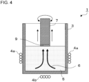
- Fig. 4 is a view showing the outlines of a crystal growing device 1 used in the production method of the present embodiment.
- the crystal growing device 1 includes a crucible 3, a pulling shaft 7, and heaters 4a and 4b (hereinafter sometimes collectively described as a heater 4).
- the crystal growing device 1 may have an internal space (hereinafter sometimes described as a "furnace") in which the crucible 3, the pulling shaft 7, and the like can be arranged, and the internal space may be capable of being kept in a sealed state.
- the heater 4 may be arranged in the internal space or may heat the internal space from the outside of it.
- the crystal growing device 1 may have a supply port (not shown in the Figure) capable of supplying various gases to the internal space, an exhaust port (not shown in the Figure) capable of discharging the gases from the internal space, a pressure gauge capable of measuring the pressure in the internal space, and the like.
- a single-crystal silicon carbide is produced by growing a crystal while bringing a seed crystal 9 of silicon carbide into contact with a raw material solution 5 including silicon and carbon from above.
- a heating step of heating a member to be used in a step of growing the crystal (hereinafter referred to as a "crystal growing step") is carried out before the crystal growing step.
- boron in the member can be reduced.
- the member may be heated in a halogen gas atmosphere. By doing so, the boron in the member can be volatilized as a boron halide.
- the member to be heated is a member including boron, and examples thereof include a crucible 3, a pulling shaft 7, and a jig for holding a seed crystal (not shown in the Figure), but in a case where there is another jig to be used, the jig may be also heated, to which the present invention is not limited.
- the halogen gas include a gas formed of single halogen such as Cl 2 and F 2 , an interhalogen gas such as ClF 3 , IF 5 , and IF 3 , and a gas containing halogen, such as HCl.
- the heating conditions are 1,600°C or higher and 2,000°C or lower for 1 to 20 hours, and a pressure of the halogen gas is 5 to 100 kPa.
- the temperature may be more preferably 1,700°C or higher and 2,000°C or lower, and still more preferably 1,800°C or higher and 2,000°C or lower.
- the heating conditions are 2,300°C or higher and 2,350°C or lower for 10 to 50 hours, and a pressure in the device is 1 to 100 kPa.
- the following temperature refers to the temperature of an object to be heated, and for example, in a case where the temperature is 1,600°C, it is heated so that the object to be heated becomes 1,600°C.
- the temperature of the object to be heated can be measured with a radiation thermometer.
- the heating step may be performed before the crystal growing step, and a timing thereof is not particularly limited. For example, after obtaining a member to be subjected to a heating treatment, a heating step of heating the member may be performed at least once before carrying out the crystal growing step using the member for the first time. Alternatively, each time the crystal growing step is performed, the heating step may also be performed immediately before performing the crystal growing step. Alternatively, the heating step may also be performed at a predetermined timing such as the start of one day, the start of one week, or the start of one month.
- the "pressure in the device" during the heating step described above can be adjusted by supplying or exhausting a gas so that the pressure in the furnace is within the above-described range.
- the "pressure of the halogen gas” refers to a pressure in the furnace in a case where only a halogen gas is supplied, and refers to a partial pressure of the halogen gas in the furnace in a case where the halogen gas and any dilution gas are supplied into the device.
- the furnace can be sealed after a gas is supplied, or a gas may be supplied and discharged at the same time to flow while maintaining a predetermined pressure.
- the gas to be supplied examples include an inert gas such as a He gas or an Ar gas, and a halogen gas.
- an H 2 gas may be used under low-reactivity conditions such as a low pressure.
- Cl 2 or HCl it is preferable to use Cl 2 or HCl since it is easy to suppress a damage and a reactivity to the member in contact with the gas.
- a separate operation may be performed to suppress an influence of the halogen gas on the seed crystal.
- the heating step is performed in a state where the seed crystal 9 is not installed, the temperature is once lowered to a workable temperature, and the seed crystal 9 is installed on the pulling shaft 7, then the next step may be performed.
- the heating step is performed, and the isolating member or the protective material is removed, then the next step may be performed.
- the temperature may not be intentionally lowered as long as the work is possible.
- a degassing step of degassing an inside of the furnace may be included between the heating step and the crystal growing step.
- the degassing method may be a known method and is not particularly limited, but vacuum degassing is preferable since the atmosphere in the furnace is efficiently removed.
- the crystal growing device 1 shown in Fig. 4 has the raw material solution 5 including silicon and carbon inside the crucible 3, and the pulling shaft 7 has a long shaft as a rotation shaft and can rotate the seed crystal 9 attached to a tip of the long shaft.
- an upward flow 6 is formed so that the raw material solution 5 flows from the bottom to the top toward the seed crystal 9.
- the centers of the crucible 3 and the pulling shaft 7 do not necessarily have to coincide, but it is preferable that the centers coincide, and it is more preferable that the center of the crucible 3, the rotation shaft of the crucible 3, the center of the pulling shaft 7, and the rotation shaft of the pulling shaft 7 all coincide.
- the crucible 3 is preferably a graphite crucible made of graphite, which can supply carbon to the raw material solution 5, but a crucible other than the graphite crucible can be used as long as a carbon source (for example, a powder or a liquid, which contains a hydrocarbon gas or carbon) can be added to the raw material solution 5 from other than the crucible.
- a carbon source for example, a powder or a liquid, which contains a hydrocarbon gas or carbon
- the rotation speed of the crucible 3 is preferably 5 to 30 rpm, and more preferably 5 to 20 rpm. By setting the ranges, the crystal growth can be efficiently performed without applying an excessive load to the device.
- the crucible 3 may be rotated reversing the rotation direction periodically in the positive direction and the opposite direction.
- the raw material solution 5 is heated by the heaters 4a and 4b, and the like provided around the crucible 3, and is maintained in a molten state.
- the heaters 4a and 4b may be of an induction heating type or a resistance heating type.
- the temperature inside the crucible 3 is preferably 1,700°C to 2,100°C.
- the temperature inside the crucible is obtained by measuring a surface of the raw material solution 5 or a vicinity thereof with a non-contact thermometer (IR-CZH7 Type manufactured by CHINO Corporation).
- silicon source of the raw material solution 5 metallic silicon, a silicon alloy, a silicon compound, or the like can be used.
- carbon source of the raw material solution a solid carbon source such as graphite, glassy carbon, and silicon carbide, a hydrocarbon gas such as methane, ethane, propane, and acetylene can be used.
- the raw material solution 5 is not particularly limited as long as it is a solution including silicon and carbon, which is used for the crystal growth of silicon carbide, but a solution in which carbon is dissolved in a Si solvent to which additive elements have been added is preferably used.
- the silicon alloy or the silicon compound used as the silicon source of the raw material solution include an alloy or compound of silicon with at least one additive element selected from Ti, Cr, Sc, Ni, Al, Co, Mn, Mg, Ge, As, P, N, O, Dy, Y, Nb, Nd, and Fe can be used.
- a Si-Cr alloy-based solvent including 20% to 60% by mole of Cr can be preferably used from the viewpoint that the solvent has a high carbon solubility, a low vapor pressure, and chemical stability.
- the inside of the crystal growing device 1 during the crystal growing step is set to be into an inert atmosphere by allowing an inert gas such as a noble gas to flow.
- the pressure is not particularly limited, but may be approximately atmospheric pressure (about 100 kPa).
- a hydrocarbon-based gas such as CH 4 may be added to form a mixed gas atmosphere.
- the gas which is a supply source of the conductive impurity may be added to provide a mixed gas atmosphere.
- the raw material solution 5 in Fig. 4 forms the upward flow 6 from bottom to top inside the crucible 3 at the center of the crucible 3, and comes into contact with the center of the seed crystal 9. It is preferable to form the upward flow 6 since the concentration of the raw material solution 5 at the growth interface can be stabilized.
- the velocity of the upward flow at a position separated by 1 cm in a downward direction from the growth interface is preferably 0.5 cm/s or more and 5 cm/s or less.
- a method of forming the upward flow 6 is not particularly limited, and a method of adjusting an output of the side surface heater 4a and the bottom surface heater 4b, a method of providing a protrusion part or plate part capable of controlling the flow in the crucible 3, a method of forming an upward flow using a Lorentz force generated by an electromagnetic field from an external magnetic field coil can be considered. For example, in a case where the output of the heater 4b on the bottom surface is increased, a convection that goes upward from the heater 4b occurs to form the upward flow 6.
- the pulling shaft 7 relatively slowly pulls the seed crystal 9 upward with respect to the raw material solution 5 to grow the single-crystal silicon carbide 11.
- the pulling shaft 7 may be moved upward or the crucible 3 may be moved downward, but it is preferable to move the pulling shaft 7 upward in order to reduce the influence on the temperature distribution relatively small.
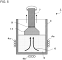
- a convex meniscus may be formed between the seed crystal 9 and the liquid surface of the raw material solution 5 in the direction of the seed crystal 9 from the liquid surface of the raw material solution 5. It is presumed that the temperature of the raw material solution 5 around the seed crystal 9 decreases by forming the meniscus, resulting in an increased degree of carbon supersaturation and an improved growth rate. In addition, since the growth rate of the seed crystal 9 in the lateral direction can be increased by adjusting the shape of the meniscus, it is possible to make the diameter of the single-crystal silicon carbide 11, which is a grown crystal, larger than the diameter of the seed crystal 9.
- the diameter of the single-crystal silicon carbide 11 may be the same as the diameter of the seed crystal 9, but as shown in Fig. 5 , the single-crystal silicon carbide 11 may also be a grown crystal so that it has a diameter larger than that of the seed crystal 9. Examples of the method for making the diameter of the grown crystal larger than the diameter of the seed crystal 9 include the method of forming a meniscus as described above.
- an angle ⁇ of the meniscus to make the diameter of the grown crystal larger is 35 degrees or more. It may be more preferably 60 degrees or more, and still more preferably 65 degrees or more. In addition, since ⁇ at a time of forming no meniscus is 90 degrees, an upper limit thereof is not particularly limited, but may be less than 90 degrees, and more preferably 85 degrees or less.
- the crystal growth may be performed while maintaining a predetermined diameter.
- the meniscus may be formed or may not be formed, but in a case where the meniscus is formed, the above-described angle ⁇ may be 10 degrees or more.
- an upper limit thereof may be set as long as the diameter of the grown crystal does not expand, but may be, for example, less than 35 degrees, and more preferably 30 degrees or less.
- the angle ⁇ of the meniscus described above is defined as an angle formed between a perpendicular line to a liquid surface l 0 passing through a point ⁇ and a liquid surface 1 on a condition where the seed crystal is viewed from a side surface.
- the point ⁇ is a contact between the end part of the grown crystal and the liquid surface.
- a crystal polymorph typified by 4H-SiC and 6H-SiC can be used.
- Fig. 6 is a schematic view of the surface of the seed crystal 9.
- the seed crystal 9 has a surface that is cut at an inclination of more than 0 degrees and 5 degrees or less with respect to the (000-1) surface, and an angle between the surface of the seed crystal 9 and the (000-1) surface is referred to as an off angle.
- the angle may be preferably 0.1 degrees or more and 5 degrees or less, and more preferably 0.5 degrees or more and 5 degrees or less.
- the seed crystal 9 having a surface cut on the (000-1) surface without providing the off angle may be used.
- the step flow direction is a direction in which the step progresses.
- the step flow direction is the [11-20] direction.
- the off angle reference may be made to Fig. 20 of International Publication No. WO2014/034080 , which is a patent document.
- the thickness of the seed crystal 9 is not particularly limited, but may be usually 0.1 mm or more.
- the thickness of the seed crystal 9 is preferably 0.3 mm or more, more preferably 1 mm or more, and still more preferably 3 mm or more, because as the thickness of the seed crystal 9 becomes thicker, the defect density of the obtained single-crystal silicon carbide 11 tends to decrease.
- the thickness of the seed crystal 9 is usually preferably 10 mm or less.
- the raw material solution 5 that comes into contact with the crystal growth surface of the seed crystal 9 needs to be in a supersaturated state.
- a cooling method in which the seed crystal 9 is immersed in the raw material solution 5 having a saturated concentration of carbon, and then the carbon concentration is brought into a supersaturated state by overcooling a temperature difference method in which the seed crystal 9 is immersed in the raw material solution 5 having a temperature gradient to grow the crystal at a low temperature part, or other methods can be used.
- the temperature difference method it is possible to precipitate the crystal of silicon carbide on the crystal growth surface of the seed crystal 9 by bringing only the vicinity of the seed crystal 9 into a supersaturated state by, for example, controlling the heating of the heater 4 or cooling by the seed crystal 9, and pulling it up under rotation at a position at which the state where the seed crystal 9 and the liquid surface of the raw material solution 5 come into contact with each other can be maintained.
- the diameter of the grown crystal can be increased by forming the meniscus at this time.
- the entire raw material solution 5 becomes supersaturated, and therefore, the crystal growth can also be caused by rotating the pulling shaft 7 in a state where the seed crystal 9 is immersed in the raw material solution 5.
- the seed crystal 9 may be left fixed, but is preferably rotated in a plane parallel to the surface of the raw material solution 5.
- the rotation speed is preferably 20 to 300 rpm, and more preferably 20 to 150 rpm.
- the rotation of the seed crystal 9 is preferably a rotation in which forward rotation and reverse rotation are repeated periodically, and the cycle thereof is about 30 seconds to 5 minutes. By changing the rotation direction periodically, the flow of the raw material solution 5 on the growth surface of the seed crystal during the crystal growth can be controlled.
- the seed crystal 9 which is an off-substrate shown in Fig. 6 is cut out to have a predetermined off angle with respect to the (000-1) surface, as described above.
- the above-described seed crystal 9 is preferably attached to the pulling shaft 7 so that the surface having an off angle is brought into contact with the raw material solution 5 as the crystal growth surface.
- a temperature T1 of a crystal growth interface P1 and a temperature T2 of a solution at the point P2 having a distance of 5 mm from the crystal growth interface P1 satisfy T2 > T1
- a temperature gradient between P1 and P2 is more than 0 K/cm and 40 K/cm or less.
- the temperature gradient is a value calculated by thermal fluid simulation.
- the lower limit value of the temperature gradient may be preferably 2 K/cm or more, and more preferably 4 K/cm or more.
- the upper limit value of the temperature gradient may be preferably 30 K/cm or less, and more preferably 20 K/cm or less.
- the single-crystal silicon carbide 11 is separated from the pulling shaft 7, and a periphery thereof is processed, as necessary, by polishing and the like, whereby a single-crystal silicon carbide ingot 21 or 22 as shown in Fig. 2(a) or Fig. 3(a) is provided.
- the crystal growth directions of the single-crystal silicon carbide ingots 21 and 22 coincide with the long shaft directions of the single-crystal silicon carbide ingots 21 and 22.
- the single-crystal silicon carbide ingots 21 and 22 may be separated from the seed crystal 9.
- the single-crystal silicon carbide wafer 31 is produced by cutting the single-crystal silicon carbide ingots 21 and 22 produced as described above.
- the single-crystal silicon carbide wafer 31 can be used as a bare wafer or provided as a seed crystal wafer for epitaxial growth.
- the crucible 3 and the pulling shaft 7 of the crystal growing device 1 as shown in Fig. 4 were heated in a halogen gas atmosphere with a pressure of a halogen gas (HCl was used in this case) in a furnace of 10 kPa at 1,800°C or higher and 2,000°C or lower for 20 hours.
- a halogen gas HCl was used in this case
- the halogen gas in the crystal growing device 1 was removed, and a disk-like 4H-SiC seed crystal having a diameter of 150 mm and a thickness of 500 ⁇ m was fixed to the lower end of a pulling shaft 7 made of carbon.
- the growth surface of the seed crystal 9 to be in contact with the solution was a C surface and offset by 1 degree from the [0001] direction to the [11-20] direction.
- the inside of the crystal growing device 1 was replaced with an atmosphere gas (He + 0.1% by volume of N 2 ), and the pressure in the device was set to 100 kPa. Furthermore, the Si-CR powder (containing 0.4% by mole of an acceptor-type element) in the crucible 3 was changed to a silicon melt by heating the heater 4, and the silicon melt was held to prepare an Si-C solution in which carbon was dissolved.
- an atmosphere gas He + 0.1% by volume of N 2
- the seed crystal 9 was brought into contact with the Si-C solution surface to grow the silicon carbide crystal from the lower end of the seed crystal 9.
- the temperature of the solution surface was set to 1,950°C, and the conditions for forming an upward flow of the solution with respect to the growth interface during the growth were used.
- the solution flow was made into a desired upward flow by control of the conditions thereof by causing a Lorentz force to act on the solution side by an electromagnetic field formed by the energization of a magnetic field coil.
- the pulling rate of the pulling shaft 7 was appropriately adjusted in accordance with the crystal growth rate, and the growing was continued until the crystal length exceeded 20 mm.
- the rotation speed of the pulling shaft 7 was controlled to a maximum of 100 rpm, and the temperature near the growth interface was controlled to 1,950°C ⁇ 20°C.
- the temperature T1 of the crystal growth interface P1 and the temperature T2 of the solution at the point P2 having a distance of 5 mm from the crystal growth interface P1 satisfy T2 > T1, and the temperature gradient between P1 and P2 was controlled to 18 K/cm.
- the temperature and the temperature gradient at the growth interface were realized by controlling an output balance of the heater that heats the crucible.
- the obtained single-crystal silicon carbide was separated from the pulling shaft.
- a central part of the separated single-crystal silicon carbide was sliced to a thickness of 500 ⁇ m at an off angle of 4 degrees with respect to the (0001) surface using a wire saw, and then the Si surface side was mirror-polished to obtain a single-crystal silicon carbide wafer.
- n-type carrier concentration was calculated, based on a difference between the concentration of the obtained donor-type conductive impurities (hereinafter also referred to as the "donor concentration") and the concentration of the acceptor-type conductive impurities (hereinafter the "acceptor concentration").
- the boron concentrations at one point at the center (central point) of the single-crystal silicon carbide wafer 31 and four points in the periphery around the center 50 mm apart from the center (peripheral point) were measured by the same method as that at the one point at the center.
- all of the obtained boron concentrations at the five points were 1.0 ⁇ 10 16 atoms/cm 3 or less.
- the evaluation value was calculated by an expression of "(Boron concentration at peripheral point - Boron concentration at central point)/Boron concentration at central point". As a result, all of the evaluation values of the four pairs were in the range of -0.3 or more and 3.0 or less.
- a basal plane dislocation density was measured by the etch pit method using KOH described above. Specifically, the single-crystal silicon carbide wafer CMP-polished on an Si surface side was immersed in a KOH melt which had been heated to 520°C for 30 minutes in an air atmosphere. After being taken out, the single-crystal silicon carbide wafer was washed with ultrapure water and used for measurement. A region within 10 cm from the center of the single-crystal silicon carbide wafer was observed. An optical microscope (BX53 manufactured by Olympus Corporation) was used for the observation, the field of view at the time of observation was set to a region of 1 cm on each four side, and the entire observation region was evaluated by scanning with a camera.
- a misorientation was measured by the above-described method at each of a total of five points of one point at the center of the single-crystal silicon carbide wafer and four points in the outer peripheral part of the wafer (0 degrees, 90 degrees, 180 degrees, and 270 degrees, each of which is a point 80% of the wafer radius apart from the center). Then, an average value of the misorientations at the five points was calculated.
- an electrical resistivity was measured at each of a total of five points of one point at the center of the single-crystal silicon carbide wafer and four points in the outer peripheral part of the wafer (0 degrees, 90 degrees, 180 degrees, and 270 degrees, each of which is a point 80% of the wafer radius apart from the center). Then, an average value of the electrical resistivities at the five points was calculated.
- Examples 1 to 4 are the single-crystal silicon carbide wafers which have the above-described Features 1 to 4, and have a low concentration of boron which is an unavoidable impurity, excellent crystallinity due to a reduction in basal plane dislocation and a reduction in misorientation, and an excellent conductivity.
- Comparative Examples 1 to 6, produced by methods different from those of Examples 1 to 4 do not have at least one of the above-described Features 1 or 2, and do not have at least one of Features 1 to 4.
- HCl was used as the halogen gas in the furnace, but the present inventors have confirmed that the same results can be obtained in a case of using other halogen gas.
Landscapes
- Chemical & Material Sciences (AREA)
- Engineering & Computer Science (AREA)
- Crystallography & Structural Chemistry (AREA)
- Materials Engineering (AREA)
- Metallurgy (AREA)
- Organic Chemistry (AREA)
- Inorganic Chemistry (AREA)
- Crystals, And After-Treatments Of Crystals (AREA)
Applications Claiming Priority (2)
| Application Number | Priority Date | Filing Date | Title |
|---|---|---|---|
| JP2021160608 | 2021-09-30 | ||
| PCT/JP2022/035724 WO2023054264A1 (fr) | 2021-09-30 | 2022-09-26 | Tranche monocristalline de carbure de silicium et lingot monocristallin de carbure de silicium |
Publications (2)
| Publication Number | Publication Date |
|---|---|
| EP4411030A1 true EP4411030A1 (fr) | 2024-08-07 |
| EP4411030A4 EP4411030A4 (fr) | 2025-10-08 |
Family
ID=85782667
Family Applications (1)
| Application Number | Title | Priority Date | Filing Date |
|---|---|---|---|
| EP22876131.8A Pending EP4411030A4 (fr) | 2021-09-30 | 2022-09-26 | Tranche monocristalline de carbure de silicium et lingot monocristallin de carbure de silicium |
Country Status (7)
| Country | Link |
|---|---|
| US (1) | US12325934B2 (fr) |
| EP (1) | EP4411030A4 (fr) |
| JP (1) | JPWO2023054264A1 (fr) |
| KR (1) | KR20240072095A (fr) |
| CN (1) | CN118043505A (fr) |
| TW (1) | TW202331031A (fr) |
| WO (1) | WO2023054264A1 (fr) |
Families Citing this family (1)
| Publication number | Priority date | Publication date | Assignee | Title |
|---|---|---|---|---|
| EP4411029A4 (fr) * | 2021-09-30 | 2025-10-22 | Central Glass Co Ltd | Tranche de carbure de silicium monocristallin, lingot de carbure de silicium monocristallin et procédé de production de carbure de silicium monocristallin |
Family Cites Families (18)
| Publication number | Priority date | Publication date | Assignee | Title |
|---|---|---|---|---|
| JP2923260B2 (ja) | 1997-03-19 | 1999-07-26 | 東洋炭素株式会社 | 単結晶引上装置、高純度黒鉛材料及びその製造方法 |
| SE525574C2 (sv) * | 2002-08-30 | 2005-03-15 | Okmetic Oyj | Lågdopat kiselkarbidsubstrat och användning därav i högspänningskomponenter |
| JP4853449B2 (ja) * | 2007-10-11 | 2012-01-11 | 住友金属工業株式会社 | SiC単結晶の製造方法、SiC単結晶ウエハ及びSiC半導体デバイス |
| JP5524855B2 (ja) | 2007-12-12 | 2014-06-18 | ダウ コーニング コーポレーション | 昇華/凝縮プロセスにより炭化ケイ素の大きな均一のインゴットを製造するための方法 |
| JP4469396B2 (ja) | 2008-01-15 | 2010-05-26 | 新日本製鐵株式会社 | 炭化珪素単結晶インゴット、これから得られる基板及びエピタキシャルウェハ |
| JP5803519B2 (ja) * | 2011-09-29 | 2015-11-04 | トヨタ自動車株式会社 | SiC単結晶の製造方法及び製造装置 |
| WO2014034080A1 (fr) | 2012-08-26 | 2014-03-06 | 国立大学法人名古屋大学 | Monocristal 3c-sic et son procédé de production |
| JP6238249B2 (ja) | 2013-05-20 | 2017-11-29 | 国立研究開発法人産業技術総合研究所 | 炭化珪素単結晶及びその製造方法 |
| JP6152981B2 (ja) | 2013-08-02 | 2017-06-28 | 株式会社デンソー | 炭化珪素単結晶 |
| JP6090287B2 (ja) | 2014-10-31 | 2017-03-08 | トヨタ自動車株式会社 | SiC単結晶の製造方法 |
| WO2017047536A1 (fr) | 2015-09-14 | 2017-03-23 | 新日鐵住金株式会社 | APPAREIL ET PROCÉDÉ DE FABRICATION DE MONOCRISTAL SiC, ET MATÉRIAU MONOCRISTALLIN SiC |
| JP6200018B2 (ja) | 2016-03-15 | 2017-09-20 | 新日鉄住金マテリアルズ株式会社 | 炭化珪素単結晶ウェハ |
| JP6845418B2 (ja) | 2017-01-13 | 2021-03-17 | セントラル硝子株式会社 | 炭化ケイ素単結晶ウェハ、インゴット及びその製造方法 |
| JP6904774B2 (ja) * | 2017-04-28 | 2021-07-21 | 富士電機株式会社 | 炭化珪素エピタキシャルウェハ、炭化珪素絶縁ゲート型バイポーラトランジスタ及びこれらの製造方法 |
| JP2021160608A (ja) | 2020-03-31 | 2021-10-11 | 株式会社エクォス・リサーチ | 移動装置 |
| EP4411029A4 (fr) * | 2021-09-30 | 2025-10-22 | Central Glass Co Ltd | Tranche de carbure de silicium monocristallin, lingot de carbure de silicium monocristallin et procédé de production de carbure de silicium monocristallin |
| CN117529584A (zh) * | 2021-10-22 | 2024-02-06 | 日本碍子株式会社 | SiC基板和SiC复合基板 |
| JP2023127894A (ja) * | 2022-03-02 | 2023-09-14 | 株式会社デンソー | 炭化珪素単結晶およびその製造方法 |
-
2022
- 2022-09-26 JP JP2023551472A patent/JPWO2023054264A1/ja active Pending
- 2022-09-26 CN CN202280066172.1A patent/CN118043505A/zh active Pending
- 2022-09-26 US US18/682,999 patent/US12325934B2/en active Active
- 2022-09-26 EP EP22876131.8A patent/EP4411030A4/fr active Pending
- 2022-09-26 WO PCT/JP2022/035724 patent/WO2023054264A1/fr not_active Ceased
- 2022-09-26 KR KR1020237045445A patent/KR20240072095A/ko active Pending
- 2022-09-30 TW TW111137382A patent/TW202331031A/zh unknown
Also Published As
| Publication number | Publication date |
|---|---|
| WO2023054264A1 (fr) | 2023-04-06 |
| CN118043505A (zh) | 2024-05-14 |
| US20240344237A1 (en) | 2024-10-17 |
| EP4411030A4 (fr) | 2025-10-08 |
| US12325934B2 (en) | 2025-06-10 |
| KR20240072095A (ko) | 2024-05-23 |
| JPWO2023054264A1 (fr) | 2023-04-06 |
| TW202331031A (zh) | 2023-08-01 |
Similar Documents
| Publication | Publication Date | Title |
|---|---|---|
| TWI410537B (zh) | Silicon carbide single crystal wafer and its manufacturing method | |
| KR101379941B1 (ko) | 탄화규소 단결정 및 탄화규소 단결정 웨이퍼 | |
| EP2752508A1 (fr) | Tranche de monocristal en carbure de silicium et son procédé de fabrication | |
| EP2059946B1 (fr) | Carbure de silicium exempt de micropipes et procede de fabrication associe | |
| KR100773624B1 (ko) | 탄화 규소 단결정으로 이루어지는 종결정 및 그를 이용한잉곳의 제조 방법 | |
| CN107002281A (zh) | 碳化硅单晶的制造方法及碳化硅单晶基板 | |
| US20190024257A1 (en) | Silicon carbide single crystal substrate and process for producing same | |
| KR20100100971A (ko) | 탄화규소 단결정의 성장방법 | |
| WO2021025085A1 (fr) | SUBSTRAT SiC, SUBSTRAT ÉPITAXIAL SiC, LINGOT DE SiC ET SES PROCÉDÉS DE PRODUCTION | |
| EP3816328A1 (fr) | Procédé de préparation d'un lingot de sic, procédé de préparation d'une tranche de sic et dispositif de préparation d'un lingot de sic | |
| EP2940196A1 (fr) | PROCÉDÉ POUR LA PRODUCTION DE MONOCRISTAL DE SiC DE TYPE n | |
| EP3051009B1 (fr) | Monocristal de sic et procédé de production de celui-ci | |
| JP2004099340A (ja) | 炭化珪素単結晶育成用種結晶と炭化珪素単結晶インゴット及びその製造方法 | |
| EP2264227A1 (fr) | Monocristal d'oxyde de zinc et son procédé de production | |
| JP4585359B2 (ja) | 炭化珪素単結晶の製造方法 | |
| EP4411030A1 (fr) | Tranche monocristalline de carbure de silicium et lingot monocristallin de carbure de silicium | |
| EP4411029A1 (fr) | Tranche de carbure de silicium monocristallin, lingot de carbure de silicium monocristallin et procédé de production de carbure de silicium monocristallin | |
| EP1498518B1 (fr) | Procede de prodution d'un monocristal de carbure de silicium | |
| JP6748613B2 (ja) | 炭化珪素単結晶基板 | |
| JP2003137694A (ja) | 炭化珪素単結晶育成用種結晶と炭化珪素単結晶インゴット及びその製造方法 | |
| TWI919007B (zh) | 碳化矽單晶體晶圓、碳化矽單晶體錠及碳化矽單晶體之製造方法 | |
| EP3243936B1 (fr) | Procédé de production d'un monocristal de sic | |
| CN113322520A (zh) | 晶片及其制造方法 | |
| WO2025249355A1 (fr) | TRANCHE DE MONOCRISTAL DE SiC, LINGOT DE MONOCRISTAL DE SiC, PROCÉDÉ DE PRODUCTION DE TRANCHE DE MONOCRISTAL DE SiC, PROCÉDÉ DE PRODUCTION DE LINGOT DE MONOCRISTAL DE SiC, DISPOSITIF DE PRODUCTION DE LINGOT DE MONOCRISTAL DE SiC ET PROCÉDÉ DE FORMATION DE FILM FORMÉ PAR CROISSANCE ÉPITAXIALE DE SiC | |
| TW202447005A (zh) | β型三氧化二鎵單晶基板、β型三氧化二鎵單晶之製造方法、及β型三氧化二鎵單晶基板之製造方法 |
Legal Events
| Date | Code | Title | Description |
|---|---|---|---|
| STAA | Information on the status of an ep patent application or granted ep patent |
Free format text: STATUS: THE INTERNATIONAL PUBLICATION HAS BEEN MADE |
|
| PUAI | Public reference made under article 153(3) epc to a published international application that has entered the european phase |
Free format text: ORIGINAL CODE: 0009012 |
|
| STAA | Information on the status of an ep patent application or granted ep patent |
Free format text: STATUS: REQUEST FOR EXAMINATION WAS MADE |
|
| 17P | Request for examination filed |
Effective date: 20240213 |
|
| AK | Designated contracting states |
Kind code of ref document: A1 Designated state(s): AL AT BE BG CH CY CZ DE DK EE ES FI FR GB GR HR HU IE IS IT LI LT LU LV MC MK MT NL NO PL PT RO RS SE SI SK SM TR |
|
| DAV | Request for validation of the european patent (deleted) | ||
| DAX | Request for extension of the european patent (deleted) | ||
| A4 | Supplementary search report drawn up and despatched |
Effective date: 20250904 |
|
| RIC1 | Information provided on ipc code assigned before grant |
Ipc: C30B 29/36 20060101AFI20250829BHEP Ipc: C30B 19/12 20060101ALI20250829BHEP Ipc: C30B 19/04 20060101ALI20250829BHEP Ipc: C30B 29/60 20060101ALI20250829BHEP |