EP4411360A1 - Mikroanalysechip - Google Patents
Mikroanalysechip Download PDFInfo
- Publication number
- EP4411360A1 EP4411360A1 EP22875959.3A EP22875959A EP4411360A1 EP 4411360 A1 EP4411360 A1 EP 4411360A1 EP 22875959 A EP22875959 A EP 22875959A EP 4411360 A1 EP4411360 A1 EP 4411360A1
- Authority
- EP
- European Patent Office
- Prior art keywords
- channel
- specimen
- time period
- working electrode
- measurement
- Prior art date
- Legal status (The legal status is an assumption and is not a legal conclusion. Google has not performed a legal analysis and makes no representation as to the accuracy of the status listed.)
- Pending
Links
Images




Classifications
-
- B—PERFORMING OPERATIONS; TRANSPORTING
- B01—PHYSICAL OR CHEMICAL PROCESSES OR APPARATUS IN GENERAL
- B01L—CHEMICAL OR PHYSICAL LABORATORY APPARATUS FOR GENERAL USE
- B01L3/00—Containers or dishes for laboratory use, e.g. laboratory glassware; Droppers
- B01L3/50—Containers for the purpose of retaining a material to be analysed, e.g. test tubes
- B01L3/502—Containers for the purpose of retaining a material to be analysed, e.g. test tubes with fluid transport, e.g. in multi-compartment structures
- B01L3/5027—Containers for the purpose of retaining a material to be analysed, e.g. test tubes with fluid transport, e.g. in multi-compartment structures by integrated microfluidic structures, i.e. dimensions of channels and chambers are such that surface tension forces are important, e.g. lab-on-a-chip
- B01L3/502753—Containers for the purpose of retaining a material to be analysed, e.g. test tubes with fluid transport, e.g. in multi-compartment structures by integrated microfluidic structures, i.e. dimensions of channels and chambers are such that surface tension forces are important, e.g. lab-on-a-chip characterised by bulk separation arrangements on lab-on-a-chip devices, e.g. for filtration or centrifugation
-
- G—PHYSICS
- G01—MEASURING; TESTING
- G01N—INVESTIGATING OR ANALYSING MATERIALS BY DETERMINING THEIR CHEMICAL OR PHYSICAL PROPERTIES
- G01N27/00—Investigating or analysing materials by the use of electric, electrochemical, or magnetic means
- G01N27/26—Investigating or analysing materials by the use of electric, electrochemical, or magnetic means by investigating electrochemical variables; by using electrolysis or electrophoresis
- G01N27/28—Electrolytic cell components
- G01N27/30—Electrodes, e.g. test electrodes; Half-cells
- G01N27/301—Reference electrodes
-
- G—PHYSICS
- G01—MEASURING; TESTING
- G01N—INVESTIGATING OR ANALYSING MATERIALS BY DETERMINING THEIR CHEMICAL OR PHYSICAL PROPERTIES
- G01N27/00—Investigating or analysing materials by the use of electric, electrochemical, or magnetic means
- G01N27/26—Investigating or analysing materials by the use of electric, electrochemical, or magnetic means by investigating electrochemical variables; by using electrolysis or electrophoresis
- G01N27/28—Electrolytic cell components
- G01N27/30—Electrodes, e.g. test electrodes; Half-cells
- G01N27/307—Disposable laminated or multilayered electrodes
-
- G—PHYSICS
- G01—MEASURING; TESTING
- G01N—INVESTIGATING OR ANALYSING MATERIALS BY DETERMINING THEIR CHEMICAL OR PHYSICAL PROPERTIES
- G01N27/00—Investigating or analysing materials by the use of electric, electrochemical, or magnetic means
- G01N27/26—Investigating or analysing materials by the use of electric, electrochemical, or magnetic means by investigating electrochemical variables; by using electrolysis or electrophoresis
- G01N27/403—Cells and electrode assemblies
- G01N27/4035—Combination of a single ion-sensing electrode and a single reference electrode
-
- B—PERFORMING OPERATIONS; TRANSPORTING
- B01—PHYSICAL OR CHEMICAL PROCESSES OR APPARATUS IN GENERAL
- B01L—CHEMICAL OR PHYSICAL LABORATORY APPARATUS FOR GENERAL USE
- B01L2200/00—Solutions for specific problems relating to chemical or physical laboratory apparatus
- B01L2200/06—Fluid handling related problems
- B01L2200/0621—Control of the sequence of chambers filled or emptied
-
- B—PERFORMING OPERATIONS; TRANSPORTING
- B01—PHYSICAL OR CHEMICAL PROCESSES OR APPARATUS IN GENERAL
- B01L—CHEMICAL OR PHYSICAL LABORATORY APPARATUS FOR GENERAL USE
- B01L2300/00—Additional constructional details
- B01L2300/06—Auxiliary integrated devices, integrated components
- B01L2300/0627—Sensor or part of a sensor is integrated
- B01L2300/0645—Electrodes
-
- B—PERFORMING OPERATIONS; TRANSPORTING
- B01—PHYSICAL OR CHEMICAL PROCESSES OR APPARATUS IN GENERAL
- B01L—CHEMICAL OR PHYSICAL LABORATORY APPARATUS FOR GENERAL USE
- B01L2300/00—Additional constructional details
- B01L2300/06—Auxiliary integrated devices, integrated components
- B01L2300/0681—Filter
-
- B—PERFORMING OPERATIONS; TRANSPORTING
- B01—PHYSICAL OR CHEMICAL PROCESSES OR APPARATUS IN GENERAL
- B01L—CHEMICAL OR PHYSICAL LABORATORY APPARATUS FOR GENERAL USE
- B01L2300/00—Additional constructional details
- B01L2300/08—Geometry, shape and general structure
- B01L2300/0861—Configuration of multiple channels and/or chambers in a single devices
- B01L2300/0877—Flow chambers
-
- B—PERFORMING OPERATIONS; TRANSPORTING
- B01—PHYSICAL OR CHEMICAL PROCESSES OR APPARATUS IN GENERAL
- B01L—CHEMICAL OR PHYSICAL LABORATORY APPARATUS FOR GENERAL USE
- B01L2300/00—Additional constructional details
- B01L2300/16—Surface properties and coatings
- B01L2300/161—Control and use of surface tension forces, e.g. hydrophobic, hydrophilic
-
- G—PHYSICS
- G01—MEASURING; TESTING
- G01N—INVESTIGATING OR ANALYSING MATERIALS BY DETERMINING THEIR CHEMICAL OR PHYSICAL PROPERTIES
- G01N27/00—Investigating or analysing materials by the use of electric, electrochemical, or magnetic means
- G01N27/26—Investigating or analysing materials by the use of electric, electrochemical, or magnetic means by investigating electrochemical variables; by using electrolysis or electrophoresis
- G01N27/28—Electrolytic cell components
- G01N27/30—Electrodes, e.g. test electrodes; Half-cells
- G01N27/333—Ion-selective electrodes or membranes
Definitions
- the present invention relates to a microanalysis chip in which a microchannel is formed inside a porous substrate.
- microanalysis chips that can efficiently perform biochemical analysis in a single chip using microsized microchannels have attracted attention in a wide range of fields. More specifically, microanalysis chips are attracting attention not only in biochemical research but also in various fields such as medicine, drug discovery, healthcare, environment, and food.
- microanalysis chips were developed that used photolithography and molds to form micron-sized microchannels on glass and silicon to perform sample pretreatment, stirring, mixing, reaction, and detection on a single chip.
- miniaturization of inspection systems, rapid analysis, and reduction of samples and waste liquid were realized.
- Electrochemical analysis measures the potential between electrodes immersed in a sample to be analyzed, and is widely used in fields such as medicine and the environment.
- Conventional electrochemical analysis is performed by engineers using sophisticated equipment, which limits the fields and resources for measurement to some extent.
- Patent Literature 1 a device including a microanalysis chip capable of potentiometric measurement using a porous substrate is proposed, and electrochemical measurement with low cost, easy handling and high disposability is possible.
- the device includes one or more working electrodes and one reference electrode on the porous substrate, and both electrodes need to be electrically connected by a fluid for potentiometric measurement.
- a high-concentration aqueous solution of KCl is used as a reference solution and dispensed into the reference electrode region including the reference electrode.
- Non-Patent Literature 1 also proposes a filter paper-based measuring device for the concentrations of Na and K ions.
- the device has a dispensing section for dispensing the sample, and the dispensed sample penetrates from the dispensing section to the respective regions of the working electrode and the reference electrode, thereby electrically connecting both electrodes and enabling potentiometric measurement.
- a KCl ion crystal is deposited on the reference electrode in order to obtain a stable potential at the reference electrode, and KCl dissolves into the sample during measurement, thereby retaining a high concentration of Cl ions in the reference electrode region and obtaining a stable potential at the reference electrode.
- only ions to be measured are selected by a K ion selective film formed to cover the working electrode, so that measurement can be performed without being affected by other ions.
- NPL 1 Nipapan Ruecha, Orawon Chailapakul, Koji Suzuki and Daniel Citterio, 'Fully Inkjet-Printed Paper-Based Potentiometric Ion-Sensing Devices', Analytical Chemistry August 29, 2017 published, 89, pp. 10,608-10,616
- the aforementioned configuration may have an impact on the sample concentration measurement accuracy. This is because, in order to obtain a stable potential at the working electrode, it takes some time to measure after the sample reaches the working electrode, but during this time, ion crystal having specimen solubility on the reference electrode flow back through the sample to the working electrode region and affect the potential of the working electrode.
- ion crystal having specimen solubility means "ion crystals soluble in the specimen” and examples thereof include KCl ion crystals.
- the present invention has an object to provide a microanalysis chip with which influence on a working electrode due to backflow of ions from a reference electrode region to a working electrode region can be suppressed and stable ion concentration measurement can be performed without increasing a chip size or prolonging a measurement time.
- a microanalysis chip including a porous substrate having provided therein a channel wall, the channel wall defining: a dispensing section to which a specimen is to be dispensed; a first channel chamber; a second channel chamber; a first channel connecting the dispensing section and the first channel chamber to each other; and a second channel connecting the dispensing section and the second channel chamber to each other, wherein the first channel chamber has a reference electrode arranged therein, the reference electrode having a surface on which an ion crystal having specimen solubility is arranged, wherein the second channel chamber has a working electrode arranged therein, and wherein the first channel and the second channel are configured so that, when a time period required for the specimen to reach the ion crystal after the specimen is dispensed to the dispensing section is represented by T1 and a time period required for the specimen to reach the working electrode after the specimen is dispensed to the dispensing section is
- a microanalysis chip capable of suppressing the influence on the working electrode due to the backflow of ions from the reference electrode region to the working electrode region without increasing the chip size or increasing the measurement time, and capable of stably measuring the ion concentration.
- a microanalysis chip of the present disclosure for solving the above-mentioned problem is described based on the following embodiments.
- the embodiments described below are merely examples, and are not intended to limit the technical scope of the present disclosure only to those embodiments.
- FIG. 1 simply shows a top view of a microanalysis chip P1.
- FIG. 2 simply shows an A-A sectional view of the microanalysis chip P1, in which a lead wire of a reference electrode 7 is omitted.
- a dispensing part 6 for dispensing a sample a flow passage chamber 1 (first flow passage chamber), a flow passage chamber 2 (second flow passage chamber), a flow passage 3 (first flow passage), and a flow passage 4 (second flow passage) are formed by a flow passage wall 5 provided inside the porous base material S1.
- the flow passage 3 connects the dispensing part 6 with the flow passage chamber 1
- the flow passage 4 connects the dispensing part 6 with the flow passage chamber 2.
- a reference electrode 7 is arranged in the flow passage chamber 1, and an ion crystal having sample solubility is arranged on the surface of the reference electrode 7.
- a working electrode 8 is arranged in the flow passage chamber 2, and the working electrode 8 is covered with an ion selective film 9 having ion selectivity.
- T1 a time period required for a specimen to reach the ion crystal 10 after the specimen is dispensed to the dispensing section 6
- T2 a time period required for the specimen to reach the working electrode 8 after the specimen is dispensed to the dispensing section 6
- T1 and T2 satisfy a relationship of T1>T2.
- microanalysis chip of the present disclosure.
- the microanalysis chip according to the present disclosure is not limited only to the configurations embodied by Examples. Further, various numerical values of a thickness, a length, a porosity, and the like are also not limited to the following values. Further, for example, when a total amount of ions in the specimen is to be measured, the ion-selective membrane 9 is not always required.
- microanalysis chip P1 according to Example 1 is described with reference to FIG. 1 and FIG. 2 .
- Example 1 resides in that, when a channel sectional area of the channel 3 (first channel) is represented by A1, and when a channel sectional area of the channel 4 (second channel) is represented by A2, the channel sectional area A1 and the channel sectional area A2 satisfy a relationship of A1 ⁇ A2.
- the channel pattern includes the dispensing section 6 to which the specimen is to be dispensed, the channel chamber 1 including the reference electrode 7, and the channel chamber 2 including the working electrode 8.
- the dispensing section 6 is connected to the channel chamber 1 by the channel 3, and is connected to the channel chamber 2 by the channel 4.
- the channel was formed so that a capacity C1 in which a specimen T was permeable is 10 ⁇ L in the channel chamber 1.
- a depth DP1 of the channel 3 and a depth DP2 of the channel 4 were set to be equal to a thickness DL1 of the porous substrate S1.
- a relationship of A1 ⁇ A2 is satisfied.
- the sectional area of the channel is adjusted by the channel width, but the present invention is not limited thereto.
- the relationship of the sectional areas is only required to be a relationship of A1 ⁇ A2.
- the channel widths W1 and W2 may be the same, and the depth DP1 of the channel 3 may be set to be smaller than the depth DP2 of the channel 4.
- sectional shape of the channel is not limited to a rectangle or a square, and may be a semicircle, a semi-ellipse, a triangle, or a trapezoid. Moreover, the sectional shape of the channel may be a polygon or a shape formed by curved surfaces without limitation.
- the sectional area of the channel is obtained by measuring an area of a cross section taken along a direction orthogonal to a direction in which the channel extends.
- porous substrate is not limited to a paper-made substrate.
- the porous substrate is only required to cause a capillary action with respect to liquid, and may be a substrate having therein a porous structure, such as an open cell structure or a network structure including a nanofiber structure.
- the porous substrate may be formed through use of resin, glass, an inorganic substrate, cloth, metal paper, or the like.
- the channel pattern was formed by heating the hydrophobic resin arranged on the porous substrate to cause the dissolved hydrophobic resin to permeate the inside of the porous substrate and fix the dissolved hydrophobic resin, but the method of forming the channel pattern is not limited thereto.
- a method of cutting the paper-made porous substrate S1 to leave only the channel shape may be employed, and as another method, the channel wall may be formed by a wax printer or the like.
- the reference electrode 7 includes, as a contact at the time of measurement, a lead wire formed by continuously extending the electrode from the inside of the channel chamber 1 onto the channel wall 5. Further, the KCl ion crystal 10 of 3.5 mg was used and arranged substantially uniformly in the entire region of the surface of the reference electrode 7.
- the working electrode 8 PEDOT:PSS (dispersion of polyethylenedioxythiophene and polystyrene sulfonate) as a main component was provided.
- the working electrode 8 also includes a lead wire formed by continuously extending the electrode from the inside of the channel chamber 2 onto the channel wall 5.
- the ion-selective membrane 9 was formed so as to cover the entire regions of the top surface and the side surface of the working electrode 8.
- the ion-selective membrane 9 was formed from the following materials.
- the reference electrode 7, the working electrode 8, and the ion-selective membrane 9 were formed in the above-mentioned shapes, sizes, materials, and the like, but the present invention is not limited thereto.
- the material of the ion crystal 10 is only required to contain Cl ions, and is not limited to KCl. Moreover, the mass of the ion crystal 10 to be arranged is only required to fall within a range of the mass that becomes a saturated solution when the ion crystal is dissolved in pure water having a volume equivalent to the capacity C1, and is not limited to 3.5 mg.
- the specimen After the specimen is dispensed to the dispensing section 6, the specimen permeates the paper-made porous substrate S1 by the capillary action in accordance with the channel pattern.
- the permeation becomes slower as the sectional area of the channel becomes narrower. This state is caused because permeation is more affected by the hydrophobic channel wall as the sectional area of the channel becomes narrower, that is, as represented by the equation (1), the permeation speed of the specimen becomes slower in the vicinity of the hydrophobic channel wall having a large contact angle ⁇ .
- the time period (reaching time to reference electrode) T1 required for the specimen to pass through the channel 3 to reach the channel chamber 1 after the specimen is dispensed to the dispensing section 6 and the time period (reaching time to working electrode) T2 required for the specimen to pass through the channel 4 to reach the channel chamber 2 after the specimen is dispensed to the dispensing section 6 have a relationship of T1>T2.
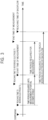
- Measurement of the specimen concentration is described with reference to FIG. 3 .
- FIG. 3 is an image diagram for illustrating a behavior of the specimen after dispensing in Example 1.
- the specimen After the specimen is dispensed to the dispensing section 6, the specimen permeates the paper-made porous substrate S1 by the capillary action in accordance with the channel pattern.
- the channel 3 connected to the channel chamber 1 including the reference electrode 7 and the channel 4 connected to the channel chamber 2 including the working electrode 8 have different configurations, and hence have different time periods required until the specimen reaches the respective channel chambers after being dispensed. That is, the reaching time to reference electrode T1 and the reaching time to working electrode T2 have a relationship of T1>T2.
- a predetermined time period is required until a measurement potential of the working electrode 8 becomes stable after the specimen reaches the working electrode 8.
- concentration measurement of the specimen can be performed, and the measurement of the specimen concentration is ended after an elapse of a predetermined measurement time period.
- Example 1 As illustrated in FIG. 3 , in Example 1, with the reaching time to reference electrode T1 and the reaching time to working electrode T2 having a relationship of T1>T2, a reaching time of backflow was able to become later than an end time of measurement. Accordingly, the measurement of the specimen concentration was able to be ended under a state in which no influence of KCl flowing backward was caused.
- Comparative Example 1-1 and Comparative Example 1-2 are given.
- FIG. 4 is an image diagram for illustrating a behavior of the specimen after the dispensing in Comparative Example 1-1.
- the reaching time to reference electrode T1 becomes earlier as compared to that of Example 1, resulting in that the reaching time of backflow also becomes earlier.
- FIG. 5 is an image diagram for illustrating a behavior of the specimen after the dispensing in Comparative Example 1-2.
- Example 1 is superior to Comparative Example 1-1 and Comparative Example 1-2 are described.
- the time period required for the specimen to reach the channel chamber after being dispensed is dependent on the sectional area of the channel.
- the volume of each channel was set as follows.
- Example 1 and Comparative Example 1 After the dispensing, in Example 1 and Comparative Example 1, the flow of the specimen to each of the working electrode and the reference electrode required a time period of about 50 seconds when the sectional area was 0.2 mm 2 , and required a time period of about 20 seconds when the sectional area was 0.5 mm 2 .
- the time period required for backflow of KCl was a time period of about 75 seconds when the channel sectional area was 0.2 mm 2 , and was a time period of about 30 seconds when the channel sectional area was 0.5 mm 2 .
- Example 1 a time period of about 50 seconds was required for the specimen to reach the reference electrode 7 from the dispensing section 6 because the channel sectional area was 0.2 mm 2 .
- a time period required for backflow of KCl to the dispensing section 6 was about 75 seconds because the channel sectional area was 0.2 mm 2 .
- a time period required for backflow to the working electrode 8 from the dispensing section was about 30 seconds because the channel sectional area was 0.5 mm 2 . That is, in Example 1, after the specimen was dispensed, a reaching time of backflow required for KCl to flow backward to reach the working electrode 8 was about 155 seconds. Similarly, the reaching time of backflow in Comparative Example 1-1 was about 80 seconds, and the reaching time of backflow in Comparative Example 1-2 was about 200 seconds.
- Table 1 shows the end time of measurement, the reaching time of backflow, and the like in Example 1 and Comparative Examples 1-1 and 1-2.
- Example 1 50 20 65 115 155 90 Comparative Example 1-1 20 20 65 - 80 15 Comparative Example 1-2 50 50 95 145 200 105
- Table 1 shows, in the configurations of Example 1 and Comparative Example 1, through use of a time at which the specimen is dispensed as a reference,
- Example 1 the measurement was able to be ended in 115 seconds, before the ion crystal KCl flowed backward to reach the working electrode.
- Comparative Example 1-2 the measurement was able to be ended before KCl reached the working electrode, but a time period further longer by 30 seconds than that in Example 1 was required until the end of the measurement.
- Example 1 the superiority of Example 1 to Comparative Example 1-1 and Comparative Example 1-2 was confirmed.
- a microanalysis chip P2 according to Example 2 is described.
- the dispensing section 6, the channel chamber 1, the channel chamber 2, the reference electrode 7, the working electrode 8, the ion-selective membrane 9, and the ion crystal 10 have configurations similar to those of the microanalysis chip P1, and hence description thereof is omitted.
- Components common to the microanalysis chip P1 are hereinafter described with common component names.
- a channel pattern of the microanalysis chip P2 is described.
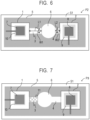
- FIG. 6 simply shows a top view of the microanalysis chip P2.
- Example 2 resides in that, when a channel volume of the channel 3 is represented by V1, and when a channel volume of the channel 4 is represented by V2, the channel volume V1 and the channel volume V2 satisfy a relationship of V1>V2.
- V1 W1 ⁇ DP1 ⁇ L1
- V2 W2 ⁇ DP2 ⁇ L2
- microanalysis chip P2 is specifically described.
- the channel volume is adjusted by the channel length, but the present invention is not limited thereto.
- the relationship of the channel volumes is only required to be V1>V2.
- the channel lengths L1 and L2 may be set to be equal to each other and the channel widths W1 and W2 may be set to be equal to each other.
- the depth DP1 of the channel 3 may be set to be deeper than the depth DP2 of the channel 4 so that V1>V2 is obtained.
- Comparative Example 2-1 Comparative Example 2-2 are given.
- Example 2 is superior to Comparative Example 2-1 and Comparative Example 2-2 are described.
- the time period required for the specimen to reach the channel chamber after being dispensed is dependent on the channel volume.
- the volume of each channel was as follows.
- the time period required until the measurement potential became stable after the specimen reached the working electrode was 45 seconds, and further, the time period required for the measurement was 50 seconds.
- the time period required for backflow of KCl was a time period of about 30 seconds when the channel volume was 6 mm 3 , and was a time period of about 60 seconds when the channel volume was 12 mm 3 .
- the reaching time of backflow was as follows.
- the time period required for the specimen to reach the reference electrode from the dispensing section was 40 seconds
- the time period required for backflow from the reference electrode to the dispensing section was 60 seconds
- the time period required for backflow from the dispensing section to the working electrode was 30 seconds.
- the reaching time of backflow was a total of 130 seconds.
- Table 2 shows the end time of measurement, the reaching time of backflow, and the like in Example 2 and Comparative Examples 2-1 and 2-2.
- Example 2 40 20 65 130 65 115 Comparative Example 2-1 20 20 65 80 15 - Comparative Example 2-2 40 40 85 160 75 135
- Table 2 shows, in the configurations of Example 2 and Comparative Example 2, through use of a time at which the specimen is dispensed as a reference,
- Example 2 the measurement was able to be ended in 115 seconds, before the ion crystal KCl flowed backward to reach the working electrode.
- Comparative Example 2-2 the measurement was able to be ended before KCl reached the working electrode, but a time period further longer by 20 seconds than that in Example 2 was required until the end of the measurement.
- the size of the microanalysis chip increased in order to ensure the channel volume.
- Example 2 With the above-mentioned evaluation, the superiority of Example 2 to Comparative Example 2-1 and Comparative Example 2-2 was confirmed.
- a microanalysis chip P3 according to Example 3 is described.
- the dispensing section 6, the channel chamber 1, the channel chamber 2, the reference electrode 7, the working electrode 8, the ion-selective membrane 9, and the ion crystal 10 have configurations similar to those of the microanalysis chip P1, and hence description thereof is omitted.
- Components common to the microanalysis chip P1 are hereinafter described with common component names.
- a channel pattern of the microanalysis chip P3 is described.
- Example 3 resides in that fine hydrophobic resin regions are formed in a dot pattern inside of the channel 3 so that the formed hydrophobic resin regions hinder permeation of the specimen.
- formed in a dot pattern means a state in which a plurality of hydrophobic resin regions are arranged apart from each other without concentrating to one location.
- Example 3 no hydrophobic resin region is formed inside of the channel 4, but the hydrophobic resin region may be formed inside of the channel 4.
- the shape of the hydrophobic resin region is not limited to a spherical shape, and may be a cuboid shape, a cube shape, or other shapes.
- FIG. 7 simply shows a top view of the microanalysis chip P3 obtained when no hydrophobic resin region is formed inside of the channel 4.
- the hydrophobic resin regions were formed only in the channel 3, but the present invention is not limited thereto.
- the hydrophobic resin region may be formed also in the channel 4.
- a hydrophobic resin was arranged on the paper-made porous substrate S1 at a portion corresponding to the channel, and then heat fixing was performed to form the hydrophobic resin region.
- the present invention is not limited thereto.
- a part or all of the hydrophobic resin regions may be formed by a wax printer or the like.
- Comparative Example 3-1 and Comparative Example 3-2 are given.
- Example 3 is superior to Comparative Example 3-1 and Comparative Example 3-2 are described.
- the hydrophobic resin regions formed inside of the channel hinder permeation of the specimen. That is, the speed of the specimen flowing through the channel can be adjusted by the hydrophobic resin regions inside of the channel.
- a time period of about 20 seconds was required for the specimen to reach each of the working electrode and the reference electrode when the number of hydrophobic resin cubes was zero, and a time period of about 80 seconds was required when the number of hydrophobic resin cubes was eight.
- the time period required until the measurement potential became stable after the specimen reached the working electrode was 45 seconds, and further, the time period required for the measurement was 50 seconds.
- Example 3 and Comparative Example 3-2 the measurement was able to be performed at a time point at which the specimen reached the reference electrode.
- a time period of about 30 seconds was required for backflow of KCl through the channel when the number of hydrophobic resin cubes was zero, and a time period of about 120 seconds was required when the number of hydrophobic resin cubes was eight.
- the reaching time of backflow was as follows.
- the time period required for the specimen to reach the reference electrode from the dispensing section was 80 seconds
- the time period required for backflow from the reference electrode to the dispensing section was 120 seconds
- the time period required for backflow from the dispensing section to the working electrode was 30 seconds.
- the reaching time of backflow was a total of 230 seconds.
- Table 3 shows the end time of measurement, the reaching time of backflow, and the like in Example 3 and Comparative Examples 3-1 and 3-2.
- Example 3 Reaching time to reference electrode T1 Reaching time to working electrode T2 Start time of measurement Reaching time of backflow Measurable time End time of measurement [second] [second] [second] [second] [second] [second] [second]]
- Example 3 80 20 80 230 150 130 Comparative Example 3-1 20 20 65 80 15 - Comparative Example 3-2 80 80 125 320 195 175
- Table 3 shows, in the configurations of Example 3 and Comparative Example 3, through use of a time at which the specimen is dispensed as a reference,
- Example 3 the measurement was able to be ended in 130 seconds, before the ion crystal KCl flowed backward to reach the working electrode.
- Example 3-2 the measurement was able to be ended before KCl reached the working electrode, but a time period further longer by 45 seconds than that in Example 3 was required until the end of the measurement.
- Example 3 With the above-mentioned evaluation, the superiority of Example 3 to Comparative Example 3-1 and Comparative Example 3-2 was confirmed.
- a microanalysis chip P4 according to Example 4 is described.
- the dispensing section 6, the channel chamber 1, the channel chamber 2, the reference electrode 7, the working electrode 8, the ion-selective membrane 9, and the ion crystal 10 have configurations similar to those of the microanalysis chip P1, and hence description thereof is omitted.
- the phrase "configurations similar” means that individual components such as the dispensing section 6, the channel chamber 1, and the channel chamber 2 are similar, and does not mean that a relative positional relationship of the individual components is similar as well.
- the microanalysis chip P4 was formed on a paper-made porous substrate S2 having permeation anisotropy as described below.
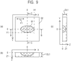
- an X axis, a Y axis, and a Z axis perpendicularly intersect with each other.
- FIG. 9(a) shows an XY plane parallel to a top surface of the paper-made porous substrate S2
- FIG. 9(b) shows an XZ plane (B-B cross section) perpendicular to the XY plane
- FIG. 9(c) shows a YZ plane (C-C cross section) perpendicular to the XY plane.
- the dispensed specimen forms a permeation shape 91 being an ellipse on the surface of the porous substrate.
- a major axis direction (X axis direction) of the ellipse matches a fiber direction F1.
- the permeation shape 91 of the specimen T had an approximate shape of a shape obtained by cutting a prolate spheroid into half along its major axis.
- the prolate spheroid means a solid of revolution obtained by rotating an ellipse about its major axis as a rotary axis.
- the maximum value that Z1 can take is the channel depth DP.
- the maximum value that Z1 can take is the thickness DL1 of the porous substrate.
- the "traveling direction of the specimen T" means a "direction in which the specimen T travels in parallel to the XY plane.”
- the specimen T After that, the specimen T reaches a channel wall surface to start spreading along the channel wall surface, and the "traveling direction of the specimen T" becomes parallel to the channel wall surface.
- Example 4 With reference to FIG. 8 , a feature of Example 4 is described.
- the feature of Example 4 is as follows.
- An arithmetic mean value of an angle formed between a major axis direction of the ellipse and a channel wall surface direction parallel to a first-channel first-wall surface 3a defining the channel 3 (first channel), and an angle formed by the major axis direction of the ellipse and a channel wall surface direction parallel to a first-channel second-wall surface 3b defining the channel 3 (first channel) is represented by an average angle r1 (0° ⁇ r1 ⁇ 90°).
- An arithmetic mean value of an angle formed between the major axis direction of the ellipse and a channel wall surface direction parallel to a second-channel first-wall surface 4a defining the channel 4 (second channel), and an angle formed between the major axis direction of the ellipse and a channel wall surface direction parallel to a second-channel second-wall surface 4b defining the channel 4 (second channel) is represented by an average angle r2 (0° ⁇ r2 ⁇ 90°).
- Example 4 resides in that the average angle r1 and the average angle r2 satisfy a relationship of r1>r2.
- the thickness DL1 was 0.1 mm, and a porosity ⁇ 1 was 50%.
- the material of the paper-made porous substrate S2 is not limited to paper, and resin, glass, an inorganic substrate, cloth, metal paper, or the like may be used.
- the porous substrate is only required be a substrate having therein a porous structure, such as an open cell structure or a network structure including a nanofiber structure, which causes a capillary action with respect to liquid and have the permeation anisotropy as described above.
- the permeation ratio E1, the thickness DL1, and the porosity ⁇ 1 of the paper-made porous substrate S2 are also not limited to the above-mentioned values.
- a channel pattern of the microanalysis chip P4 is described.
- FIG. 8 simply shows a top view of an example of the microanalysis chip P4.
- Example 4 resides in that, in a case in which the fiber direction F1 is regarded as 0°, when the average angle of the channel 3 is represented by r1 (0° ⁇ r1 ⁇ 90°) and the average angle of the channel 4 is represented by r2 (0° ⁇ r2 ⁇ 90°), r1>r2 is satisfied.
- the fiber direction F1 is the same direction as the major axis direction of the permeation shape being the ellipse formed on the surface of the porous substrate by the specimen dispensed to the porous substrate.
- Comparative Example 4-1 and Comparative Example 4-2 are given.
- Example 4 is superior to Comparative Example 4-1 and Comparative Example 4-2 are described.
- the time period required for the specimen to reach the channel chamber after being dispensed is dependent on the average angle of the channel with respect to the fiber direction, even in the case of the same channel volume.
- the "average angle of the channel with respect to the fiber direction” is hereinafter also referred to as "average angle of the channel.”
- the channel pattern was formed on the paper-made porous substrate S2 having permeation anisotropy in which the permeation ratio E1 in the major and minor axis directions was twice as large.
- the fiber direction F 1 is regarded as 0°
- a time period in which the specimen travels in a direction of 90° is twice as long as a time period in which the specimen travels in a direction of 0° by the same distance.
- a time period required until the specimen reached the channel chamber (electrode) after being dispensed was a time period of about 20 seconds when the average angle of the channel was 0°, and was a time period of about 40 seconds when the average angle of the channel was 90°.
- the time period required until the measurement potential became stable after the specimen reached the working electrode was 45 seconds, and further, the time period required for the measurement was 50 seconds.
- the time period required for backflow of KCl through the channel was a time period of about 30 seconds when the average angle of the channel was 0°, and was a time period of about 60 seconds when the average angle of the channel was 90°.
- Example 4 the reaching time of backflow was as follows.
- the time period required for the specimen to reach the reference electrode from the dispensing section was 40 (sec)
- the time period required for backflow from the reference electrode to the dispensing section was 60 seconds
- the time period required for backflow from the dispensing section to the working electrode was 30 seconds.
- the reaching time of backflow was a total of 130 seconds.
- Table 4 shows the end time of measurement, the reaching time of backflow, and the like in Example 4 and Comparative Examples 4-1 and 4-2.
- Example 4 40 20 65 130 65 115 Comparative Example 4-1 20 20 65 80 15 - Comparative Example 4-2 40 40 85 160 75 135
- Table 4 shows, in the configurations of Example 4 and Comparative Example 4, through use of a time at which the specimen is dispensed as a reference,
- Example 4 the measurement was able to be ended in 115 seconds, and the time at which the measurement was ended was earlier than the time at which the ion crystal KCl flowed backward to reach the working electrode.
Landscapes
- Chemical & Material Sciences (AREA)
- Health & Medical Sciences (AREA)
- Life Sciences & Earth Sciences (AREA)
- Analytical Chemistry (AREA)
- Molecular Biology (AREA)
- Chemical Kinetics & Catalysis (AREA)
- General Health & Medical Sciences (AREA)
- Biochemistry (AREA)
- Physics & Mathematics (AREA)
- Electrochemistry (AREA)
- General Physics & Mathematics (AREA)
- Immunology (AREA)
- Pathology (AREA)
- Dispersion Chemistry (AREA)
- Hematology (AREA)
- Clinical Laboratory Science (AREA)
- Automatic Analysis And Handling Materials Therefor (AREA)
- Physical Or Chemical Processes And Apparatus (AREA)
- Sampling And Sample Adjustment (AREA)
Applications Claiming Priority (2)
| Application Number | Priority Date | Filing Date | Title |
|---|---|---|---|
| JP2021158506A JP7755429B2 (ja) | 2021-09-28 | 2021-09-28 | マイクロ分析チップ |
| PCT/JP2022/035095 WO2023054092A1 (ja) | 2021-09-28 | 2022-09-21 | マイクロ分析チップ |
Publications (2)
| Publication Number | Publication Date |
|---|---|
| EP4411360A1 true EP4411360A1 (de) | 2024-08-07 |
| EP4411360A4 EP4411360A4 (de) | 2025-08-13 |
Family
ID=85779847
Family Applications (1)
| Application Number | Title | Priority Date | Filing Date |
|---|---|---|---|
| EP22875959.3A Pending EP4411360A4 (de) | 2021-09-28 | 2022-09-21 | Mikroanalysechip |
Country Status (5)
| Country | Link |
|---|---|
| US (1) | US20240238785A1 (de) |
| EP (1) | EP4411360A4 (de) |
| JP (2) | JP7755429B2 (de) |
| CN (1) | CN118019973A (de) |
| WO (1) | WO2023054092A1 (de) |
Cited By (1)
| Publication number | Priority date | Publication date | Assignee | Title |
|---|---|---|---|---|
| EP4509826A4 (de) * | 2022-04-12 | 2026-04-15 | Canon Kk | Mikroanalysechip |
Families Citing this family (5)
| Publication number | Priority date | Publication date | Assignee | Title |
|---|---|---|---|---|
| WO2024202078A1 (ja) | 2023-03-24 | 2024-10-03 | Dic株式会社 | 付加重合反応に係る予測を行う方法、情報処理装置、及びプログラム |
| CN121057938A (zh) * | 2023-05-10 | 2025-12-02 | 佳能株式会社 | 分析器件和电解质浓度测量方法 |
| EP4729934A1 (de) * | 2023-06-13 | 2026-04-22 | Canon Kabushiki Kaisha | Analysegerät |
| WO2025142287A1 (ja) * | 2023-12-25 | 2025-07-03 | 株式会社堀場アドバンスドテクノ | イオン分析装置及びイオン分析方法 |
| WO2025216222A1 (ja) * | 2024-04-09 | 2025-10-16 | キヤノン株式会社 | 分析デバイスシート |
Family Cites Families (8)
| Publication number | Priority date | Publication date | Assignee | Title |
|---|---|---|---|---|
| JPS58156848A (ja) * | 1982-03-15 | 1983-09-17 | Fuji Photo Film Co Ltd | イオン選択電極及びその製造法 |
| US7723099B2 (en) | 2003-09-10 | 2010-05-25 | Abbott Point Of Care Inc. | Immunoassay device with immuno-reference electrode |
| US8021529B2 (en) * | 2005-04-20 | 2011-09-20 | Thermo Orion, Inc. | Ion measurement/calibration cell |
| WO2013036617A1 (en) | 2011-09-06 | 2013-03-14 | President And Fellows Of Harvard College | Microfluidic devices for multiplexed electrochemical detection |
| JP2014006086A (ja) | 2012-06-21 | 2014-01-16 | Sharp Corp | イオンセンサおよびイオンセンサの製造方法 |
| US20160033438A1 (en) | 2013-03-15 | 2016-02-04 | President And Fellows Of Harvard College | Paper-Based Reference Electrode And Potentiometric Ion Sensing |
| KR102447394B1 (ko) * | 2015-12-03 | 2022-09-27 | 프리시젼바이오 주식회사 | 유체분석 카트리지 및 이를 포함하는 유체분석장치 |
| JP7519796B2 (ja) | 2020-03-26 | 2024-07-22 | アイホン株式会社 | インターホン機器 |
-
2021
- 2021-09-28 JP JP2021158506A patent/JP7755429B2/ja active Active
-
2022
- 2022-09-21 WO PCT/JP2022/035095 patent/WO2023054092A1/ja not_active Ceased
- 2022-09-21 EP EP22875959.3A patent/EP4411360A4/de active Pending
- 2022-09-21 CN CN202280064786.6A patent/CN118019973A/zh active Pending
-
2024
- 2024-03-27 US US18/618,542 patent/US20240238785A1/en active Pending
-
2025
- 2025-08-28 JP JP2025142631A patent/JP2025161994A/ja active Pending
Cited By (1)
| Publication number | Priority date | Publication date | Assignee | Title |
|---|---|---|---|---|
| EP4509826A4 (de) * | 2022-04-12 | 2026-04-15 | Canon Kk | Mikroanalysechip |
Also Published As
| Publication number | Publication date |
|---|---|
| JP2023048922A (ja) | 2023-04-07 |
| WO2023054092A1 (ja) | 2023-04-06 |
| EP4411360A4 (de) | 2025-08-13 |
| US20240238785A1 (en) | 2024-07-18 |
| CN118019973A (zh) | 2024-05-10 |
| JP2025161994A (ja) | 2025-10-24 |
| JP7755429B2 (ja) | 2025-10-16 |
Similar Documents
| Publication | Publication Date | Title |
|---|---|---|
| EP4411360A1 (de) | Mikroanalysechip | |
| EP4411361A1 (de) | Mikroanalysechip, elektrolytkonzentrationsmesssystem und elektrolytkonzentrationsmessverfahren | |
| US20250067700A1 (en) | Microanalytical chip | |
| EP4509826A1 (de) | Mikroanalysechip | |
| US20240238780A1 (en) | Micro-analysis chip | |
| US20250052714A1 (en) | Microchannel device | |
| JP2024163046A (ja) | 分析デバイス及び電解質濃度測定方法 | |
| EP4711752A1 (de) | Analysevorrichtung und elektrolytkonzentrationsmessverfahren | |
| JP6925085B1 (ja) | 電気化学センサユニット | |
| EP4682528A1 (de) | Verfahren zur messung der elektrolytkonzentration | |
| US20260092890A1 (en) | Analytical device | |
| US20250303408A1 (en) | Micro-analysis chip, electrolyte concentration measuring system, and electrolyte concentration measuring method | |
| JP2025162416A (ja) | 分析デバイス及び分析方法 | |
| JP2024178899A (ja) | 分析デバイス | |
| JP2025159972A (ja) | 分析デバイス及び分析デバイスを用いた検査方法 | |
| JP2024179067A (ja) | 分析デバイス |
Legal Events
| Date | Code | Title | Description |
|---|---|---|---|
| STAA | Information on the status of an ep patent application or granted ep patent |
Free format text: STATUS: THE INTERNATIONAL PUBLICATION HAS BEEN MADE |
|
| PUAI | Public reference made under article 153(3) epc to a published international application that has entered the european phase |
Free format text: ORIGINAL CODE: 0009012 |
|
| STAA | Information on the status of an ep patent application or granted ep patent |
Free format text: STATUS: REQUEST FOR EXAMINATION WAS MADE |
|
| 17P | Request for examination filed |
Effective date: 20240429 |
|
| AK | Designated contracting states |
Kind code of ref document: A1 Designated state(s): AL AT BE BG CH CY CZ DE DK EE ES FI FR GB GR HR HU IE IS IT LI LT LU LV MC MK MT NL NO PL PT RO RS SE SI SK SM TR |
|
| DAV | Request for validation of the european patent (deleted) | ||
| DAX | Request for extension of the european patent (deleted) | ||
| A4 | Supplementary search report drawn up and despatched |
Effective date: 20250714 |
|
| RIC1 | Information provided on ipc code assigned before grant |
Ipc: G01N 27/30 20060101AFI20250708BHEP Ipc: G01N 27/403 20060101ALI20250708BHEP Ipc: B01L 3/00 20060101ALI20250708BHEP Ipc: G01N 27/333 20060101ALI20250708BHEP |