EP4421588A1 - Dispositif électronique avec une batterie à étages - Google Patents
Dispositif électronique avec une batterie à étages Download PDFInfo
- Publication number
- EP4421588A1 EP4421588A1 EP23181617.4A EP23181617A EP4421588A1 EP 4421588 A1 EP4421588 A1 EP 4421588A1 EP 23181617 A EP23181617 A EP 23181617A EP 4421588 A1 EP4421588 A1 EP 4421588A1
- Authority
- EP
- European Patent Office
- Prior art keywords
- bent part
- circuit board
- substrate body
- electronic device
- electrical connection
- Prior art date
- Legal status (The legal status is an assumption and is not a legal conclusion. Google has not performed a legal analysis and makes no representation as to the accuracy of the status listed.)
- Pending
Links
Images


Classifications
-
- G—PHYSICS
- G09—EDUCATION; CRYPTOGRAPHY; DISPLAY; ADVERTISING; SEALS
- G09F—DISPLAYING; ADVERTISING; SIGNS; LABELS OR NAME-PLATES; SEALS
- G09F9/00—Indicating arrangements for variable information in which the information is built-up on a support by selection or combination of individual elements
- G09F9/30—Indicating arrangements for variable information in which the information is built-up on a support by selection or combination of individual elements in which the desired character or characters are formed by combining individual elements
-
- G—PHYSICS
- G06—COMPUTING OR CALCULATING; COUNTING
- G06F—ELECTRIC DIGITAL DATA PROCESSING
- G06F1/00—Details not covered by groups G06F3/00 - G06F13/00 and G06F21/00
- G06F1/16—Constructional details or arrangements
- G06F1/1613—Constructional details or arrangements for portable computers
- G06F1/1633—Constructional details or arrangements of portable computers not specific to the type of enclosures covered by groups G06F1/1615 - G06F1/1626
- G06F1/1637—Details related to the display arrangement, including those related to the mounting of the display in the housing
-
- G—PHYSICS
- G06—COMPUTING OR CALCULATING; COUNTING
- G06F—ELECTRIC DIGITAL DATA PROCESSING
- G06F1/00—Details not covered by groups G06F3/00 - G06F13/00 and G06F21/00
- G06F1/16—Constructional details or arrangements
- G06F1/1613—Constructional details or arrangements for portable computers
- G06F1/1626—Constructional details or arrangements for portable computers with a single-body enclosure integrating a flat display, e.g. Personal Digital Assistants [PDAs]
-
- G—PHYSICS
- G06—COMPUTING OR CALCULATING; COUNTING
- G06F—ELECTRIC DIGITAL DATA PROCESSING
- G06F1/00—Details not covered by groups G06F3/00 - G06F13/00 and G06F21/00
- G06F1/16—Constructional details or arrangements
- G06F1/1613—Constructional details or arrangements for portable computers
- G06F1/1615—Constructional details or arrangements for portable computers with several enclosures having relative motions, each enclosure supporting at least one I/O or computing function
- G06F1/1616—Constructional details or arrangements for portable computers with several enclosures having relative motions, each enclosure supporting at least one I/O or computing function with folding flat displays, e.g. laptop computers or notebooks having a clamshell configuration, with body parts pivoting to an open position around an axis parallel to the plane they define in closed position
-
- G—PHYSICS
- G06—COMPUTING OR CALCULATING; COUNTING
- G06F—ELECTRIC DIGITAL DATA PROCESSING
- G06F1/00—Details not covered by groups G06F3/00 - G06F13/00 and G06F21/00
- G06F1/16—Constructional details or arrangements
- G06F1/1613—Constructional details or arrangements for portable computers
- G06F1/1633—Constructional details or arrangements of portable computers not specific to the type of enclosures covered by groups G06F1/1615 - G06F1/1626
- G06F1/1635—Details related to the integration of battery packs and other power supplies such as fuel cells or integrated AC adapter
-
- G—PHYSICS
- G06—COMPUTING OR CALCULATING; COUNTING
- G06F—ELECTRIC DIGITAL DATA PROCESSING
- G06F1/00—Details not covered by groups G06F3/00 - G06F13/00 and G06F21/00
- G06F1/16—Constructional details or arrangements
- G06F1/1613—Constructional details or arrangements for portable computers
- G06F1/1633—Constructional details or arrangements of portable computers not specific to the type of enclosures covered by groups G06F1/1615 - G06F1/1626
- G06F1/1637—Details related to the display arrangement, including those related to the mounting of the display in the housing
- G06F1/1652—Details related to the display arrangement, including those related to the mounting of the display in the housing the display being flexible, e.g. mimicking a sheet of paper, or rollable
-
- G—PHYSICS
- G06—COMPUTING OR CALCULATING; COUNTING
- G06F—ELECTRIC DIGITAL DATA PROCESSING
- G06F1/00—Details not covered by groups G06F3/00 - G06F13/00 and G06F21/00
- G06F1/16—Constructional details or arrangements
- G06F1/1613—Constructional details or arrangements for portable computers
- G06F1/1633—Constructional details or arrangements of portable computers not specific to the type of enclosures covered by groups G06F1/1615 - G06F1/1626
- G06F1/1656—Details related to functional adaptations of the enclosure, e.g. to provide protection against EMI, shock, water, or to host detachable peripherals like a mouse or removable expansions units like PCMCIA cards, or to provide access to internal components for maintenance or to removable storage supports like CDs or DVDs, or to mechanically mount accessories
-
- H—ELECTRICITY
- H04—ELECTRIC COMMUNICATION TECHNIQUE
- H04M—TELEPHONIC COMMUNICATION
- H04M1/00—Substation equipment, e.g. for use by subscribers
- H04M1/02—Constructional features of telephone sets
- H04M1/0202—Portable telephone sets, e.g. cordless phones, mobile phones or bar type handsets
- H04M1/0206—Portable telephones comprising a plurality of mechanically joined movable body parts, e.g. hinged housings
- H04M1/0208—Portable telephones comprising a plurality of mechanically joined movable body parts, e.g. hinged housings characterized by the relative motions of the body parts
- H04M1/0214—Foldable telephones, i.e. with body parts pivoting to an open position around an axis parallel to the plane they define in closed position
- H04M1/0216—Foldable in one direction, i.e. using a one degree of freedom hinge
-
- H—ELECTRICITY
- H04—ELECTRIC COMMUNICATION TECHNIQUE
- H04M—TELEPHONIC COMMUNICATION
- H04M1/00—Substation equipment, e.g. for use by subscribers
- H04M1/02—Constructional features of telephone sets
- H04M1/0202—Portable telephone sets, e.g. cordless phones, mobile phones or bar type handsets
- H04M1/026—Details of the structure or mounting of specific components
- H04M1/0262—Details of the structure or mounting of specific components for a battery compartment
-
- H—ELECTRICITY
- H04—ELECTRIC COMMUNICATION TECHNIQUE
- H04M—TELEPHONIC COMMUNICATION
- H04M1/00—Substation equipment, e.g. for use by subscribers
- H04M1/02—Constructional features of telephone sets
- H04M1/0202—Portable telephone sets, e.g. cordless phones, mobile phones or bar type handsets
- H04M1/026—Details of the structure or mounting of specific components
- H04M1/0266—Details of the structure or mounting of specific components for a display module assembly
-
- H—ELECTRICITY
- H04—ELECTRIC COMMUNICATION TECHNIQUE
- H04M—TELEPHONIC COMMUNICATION
- H04M1/00—Substation equipment, e.g. for use by subscribers
- H04M1/02—Constructional features of telephone sets
- H04M1/0202—Portable telephone sets, e.g. cordless phones, mobile phones or bar type handsets
- H04M1/026—Details of the structure or mounting of specific components
- H04M1/0266—Details of the structure or mounting of specific components for a display module assembly
- H04M1/0268—Details of the structure or mounting of specific components for a display module assembly including a flexible display panel
-
- H—ELECTRICITY
- H04—ELECTRIC COMMUNICATION TECHNIQUE
- H04M—TELEPHONIC COMMUNICATION
- H04M1/00—Substation equipment, e.g. for use by subscribers
- H04M1/02—Constructional features of telephone sets
- H04M1/0202—Portable telephone sets, e.g. cordless phones, mobile phones or bar type handsets
- H04M1/026—Details of the structure or mounting of specific components
- H04M1/0277—Details of the structure or mounting of specific components for a printed circuit board assembly
-
- H—ELECTRICITY
- H05—ELECTRIC TECHNIQUES NOT OTHERWISE PROVIDED FOR
- H05K—PRINTED CIRCUITS; CASINGS OR CONSTRUCTIONAL DETAILS OF ELECTRIC APPARATUS; MANUFACTURE OF ASSEMBLAGES OF ELECTRICAL COMPONENTS
- H05K1/00—Printed circuits
- H05K1/02—Details
- H05K1/14—Structural association of two or more printed circuits
- H05K1/147—Structural association of two or more printed circuits at least one of the printed circuits being bent or folded, e.g. by using a flexible printed circuit
-
- H—ELECTRICITY
- H05—ELECTRIC TECHNIQUES NOT OTHERWISE PROVIDED FOR
- H05K—PRINTED CIRCUITS; CASINGS OR CONSTRUCTIONAL DETAILS OF ELECTRIC APPARATUS; MANUFACTURE OF ASSEMBLAGES OF ELECTRICAL COMPONENTS
- H05K1/00—Printed circuits
- H05K1/18—Printed circuits structurally associated with non-printed electric components
- H05K1/189—Printed circuits structurally associated with non-printed electric components characterised by the use of flexible or folded printed circuits
-
- H—ELECTRICITY
- H05—ELECTRIC TECHNIQUES NOT OTHERWISE PROVIDED FOR
- H05K—PRINTED CIRCUITS; CASINGS OR CONSTRUCTIONAL DETAILS OF ELECTRIC APPARATUS; MANUFACTURE OF ASSEMBLAGES OF ELECTRICAL COMPONENTS
- H05K5/00—Casings, cabinets or drawers for electric apparatus
- H05K5/02—Details
-
- H—ELECTRICITY
- H05—ELECTRIC TECHNIQUES NOT OTHERWISE PROVIDED FOR
- H05K—PRINTED CIRCUITS; CASINGS OR CONSTRUCTIONAL DETAILS OF ELECTRIC APPARATUS; MANUFACTURE OF ASSEMBLAGES OF ELECTRICAL COMPONENTS
- H05K2201/00—Indexing scheme relating to printed circuits covered by H05K1/00
- H05K2201/05—Flexible printed circuits [FPCs]
Definitions
- the present disclosure relates to a field of terminals, and more particularly to an electronic device.
- the level of intelligence and integration of the devices also improves.
- power consumption of the internal modules increases which, in turn, causes increased demand for battery capacity in order to enhance the endurance time of the device.
- the present disclosure provides a display screen and an electronic device to solve the deficiencies in the related art.
- an electronic device includes: a display screen including an array substrate, the array substrate including a substrate body and a bent part connected with a first side surface of the substrate body, and the bent part being bent towards a non-display side of the display screen; a first support plate connected with the substrate body and cooperating with a part of the substrate body to define a first accommodating cavity, and the bent part being partially located in the first accommodating cavity; and a flexible circuit board arranged in the first accommodating cavity, and connected with and in conduction with the bent part, and the flexible circuit board being at least partially arranged between the substrate body and the bent part.
- the first support plate includes a support body, a transition part and a step part, the transition part connects the support body with the step part, and the support body and the step part are spaced apart by a preset height in a thickness direction of the electronic device;
- the support body is connected with the substrate body, one side surface of the step part, one side surface of the transition part and the part of the substrate body define the first accommodating cavity, and another opposite side surface of the step part, another opposite side surface of the transition part and the support body define a second accommodating cavity;
- the electronic device further includes a stepped battery arranged on a side surface of the first support plate facing away from a display side of the display screen, and the stepped battery is partially arranged in the second accommodating cavity.
- the bent part includes a first electrical connection region, and the first electrical connection region is located at a side of the bent part facing away from the substrate body; and the flexible circuit board is connected with the first electrical connection region, extends away from the bent part, wraps an edge of the bent part and is folded into a space between the substrate body and the bent part.
- the bent part includes a first electrical connection region, the first electrical connection region is located at a side of the bent part facing away from the substrate body, and the bent part includes a conductive via hole;
- the flexible circuit board includes a first circuit board and a second circuit board, and the first circuit board is in conduction with the first electrical connection region;
- the second circuit board is at least partially located between the substrate body and the bent part, and is in conduction with the first electrical connection region through the conductive via hole.
- the bent part includes a first electrical connection region, and the first electrical connection region is located at a side of the bent part facing away from the substrate body; and the flexible circuit board includes a third circuit board and a fourth circuit board, the third circuit board is connected with and in conduction with the first electrical connection region, the fourth circuit board is connected with and in conduction with the third circuit board, and the fourth circuit board is at least partially located between the substrate body and the bent part.
- the bent part includes a first electrical connection region and a second electrical connection region, the first electrical connection region is located at a side of the bent part facing away from the substrate body, and the second electrical connection region is located at a side of the bent part facing the substrate body; and the flexible circuit board includes a fifth circuit board and a sixth circuit board, the fifth circuit board is connected with and in conduction with the first electrical connection region, the sixth circuit board is connected with and in conduction with the second connection region, and the sixth circuit board is at least partially located between the substrate body and the bent part.
- the bent part includes a second electrical connection region, and the second electrical connection region is located at a side of the bent part facing the substrate body; and a region of the flexible circuit board arranged between the substrate body and the bent part is in conduction with the second electrical connection region.
- a maximum height of the flexible circuit board is lower than a minimum height of the bent part.
- the first support plate includes a second avoidance part in communication with the first accommodating cavity; and the electronic device further includes a chip assembly, the chip assembly is arranged on a surface of the bent part facing away from the substrate body, and the chip assembly is at least partially located in the second avoidance part.
- the electronic device further includes a chip assembly, the chip assembly includes a first chip and a second chip, and both the first chip and the second chip are arranged on a portion of the bent part parallel to the substrate body.
- the first chip and the second chip are symmetrically arranged relative to a center line of the bent part, and an extension direction of the center line is perpendicular to the first side surface.
- the electronic device further includes: a second support plate connected with the substrate body; and a rotating shaft.
- the second support plate is connected to one side of the rotating shaft, and the first support plate is connected to the other side of the rotating shaft.
- the second support plate and the first support plate are configured to move close to or away from each other along with rotation of the rotating shaft, to allow the electronic device to be switched between an unfolded state and a folded state.
- the present disclosure can utilize the space formed between the bent part and the substrate body when the bent part is bent to arrange the part of the flexible circuit board, without raising higher requirements on the volume of the first accommodating cavity, and also, it is beneficial to reducing the width of the flexible circuit board, thus reducing the size of the first accommodating cavity, thus reducing the overall volume of the first accommodating cavity, and increasing the contact area between the first support plate and the display screen, so as to increase the strength of the display screen.
- first, second and third are used herein for the purpose of describing various information, but such information should not be limited to these terms. These terms are only used to distinguish the same type of information from each other.
- first information may also be called the second information, and similarly, the second information may also be called the first information.
- word “if' as used herein may be interpreted as “while” or “when” or “in response to determining”.
- a support plate 103 is arranged at one side of a display screen to support the display screen, so as to enhance the strength of the display screen, and a flexible printed circuit (FPC) 102 and a Chip on PI (COP) IC 101 of the screen are arranged under a local portion of the support plate 103. Since the FPC and the COP need to occupy space, and the FPC extends towards the support plate 103 in a horizontal direction in Fig. 2 , which needs to occupy a large area, a large region of the display screen cannot be supported by the support plate 103, and the strength of the display screen is weakened.
- FPC flexible printed circuit
- COP Chip on PI
- the present disclosure provides an electronic device 200, and the electronic device 200 may include a display screen 1, a first support plate 2 and a stepped battery 3.
- the display screen 1 may include an array substrate 11 and a display layer 12, and the display layer 12 is arranged on a surface of the array substrate 11.
- the array substrate 11 may include a substrate element and a thin film transistor layer, and the substrate element may be a flexible substrate element.
- the array substrate 11 includes a substrate body 111 and a bent part 112 connected with a first side surface of the substrate body 111.
- the substrate body 111 may be connected to the display layer 12, and the display layer 12 is supported and protected by the substrate body 111.
- the bent part 112 is located at an outer side relative to the substrate body 111, so that the bent part 112 may bend towards a non-display side of the display screen 1 and wrap an edge of the first side surface the substrate body 111.
- the first support plate 2 is connected with the substrate body 111. Specifically, the first support plate 2 may be connected and fixed with the substrate body 111 by an adhesive, and the first support plate 2 and the substrate body 111 may define an open first accommodating cavity 4.
- the bent part 112 may extend into the first accommodating cavity 4 after being bent and wrapping the edge (for example, an upper edge in Figs. 3-7 ) of the first side surface of the substrate body 111, so that a portion of the bent part 112 may be located in the first accommodating cavity 4.
- the electronic device 200 may further include a flexible circuit board 6, which is arranged in the first accommodating cavity 4, and connected with and in conduction with the bent part 112. At least a part of the flexible circuit board 6 may be bonded with the substrate body 111 by an adhesive, and the bent part 112 may be indirectly fixed on the substrate body 111 by the flexible circuit board 6, or the bent part 112 may be directly connected and fixed with the substrate body 111 by an adhesive, which may be designed as required, and is not limited by the present disclosure.
- An area occupied by the flexible circuit board 6 in the first accommodating cavity 4 will directly affect a volume of the first accommodating cavity 4, and further affect a contact area between the first support plate 2 and the substrate body 111.
- the flexible circuit board 6 may be at least partially arranged between the substrate body 111 and the bent part 112, so that a part of the flexible circuit board 6 may be arranged in a space formed between the bent part 112 and the substrate body 111 when the bent part 112 is bent, without raising higher requirements on the volume of the first accommodating cavity 4, and also, it is beneficial to reducing a size of the flexible circuit board 6 in a horizontal direction in Fig. 3 , i.e., reducing a width of the flexible circuit board 6. Therefore, a size of the first accommodating cavity 4 in the horizontal direction of Fig. 3 can be reduced, without increasing a size of the first accommodating cavity 4 in a vertical direction of Fig. 3 , so that the overall volume of the first accommodating cavity 4 is reduced, which is beneficial to increasing the contact area between the first support plate 2 and the display screen 1, thereby improving the strength of the display screen 1.
- the battery is arranged above the support plate 103, and its side adjacent to the support plate 103 is flat, so that the space utilization rate is not good, and the battery capacity cannot be optimized to a greater extent to improve the endurance capacity of the device.
- the first support plate 2 may include a support body 21, a transition part 22 and a step part 23.
- One end of the transition part 22 is connected with the support body 21 and the other end of the transition part 22 is connected with the step part 23.
- the support body 21 and the step part 23 are spaced apart from each other by a preset distance in a thickness direction of the electronic device 200, and the preset distance is equal to a height of the transition part 22 in the thickness direction of the electronic device 200.
- the support body 21 may be connected to a second side surface (which is connected with and perpendicular to the first side surface) of the substrate body 111 facing away from the display layer 12, for example, bonded to the substrate body 111 by a double-sided adhesive tape, and the strength of the display screen 1 is further improved by the support body 21.
- a side surface of the transition part 22, a side surface of the step part 23 and a part of the substrate body 111 may define the first accommodating cavity 4, and the bent part 112 may extend into the first accommodating cavity 4 after being bent and wrapping the edge of the first side surface of the substrate body 111, so that the portion of the bent part 112 may be located in the first accommodating cavity 4.
- the support body 21 and the step part 23 have a height difference therebetween, so that another opposite side surface of the transition part 22, another opposite side surface of the step part 23 and the support body 21 may cooperate to define a second accommodating cavity 5, and the stepped battery 3 may be arranged on a side surface of the first support plate 2 facing away from the display screen 1, and partially arranged in the second accommodating cavity 5.
- the stepped battery 3 since the stepped battery 3 may be partially arranged in the second accommodating cavity 5, the volume of the stepped battery 3 can be increased, the capacity of the stepped battery 3 can be improved, and the endurance time of the electronic device 200 can be prolonged.
- the second accommodating cavity 5 may also have a shape of a groove, and this is not limited in the present disclosure.
- the transition part 22 of the first support plate 2 can be arranged more adjacent to the bent part 112, so that the volume of the second accommodating cavity 5 can be increased, which is beneficial to further improving the capacity of the stepped battery 3.
- the part of the flexible circuit board 6 arranged between the substrate body 111 and the bent part 112 may be realized in various ways.
- the bent part 112 may include a first electrical connection region 113, which is located at a side of the bent part 112 facing away from the substrate body 111.
- the flexible circuit board 6 has a monolithic design, and may wrap an edge of the bent part 112 and be folded into a space between the substrate body 111 and the bent part 112, thereby reducing the width of the flexible circuit board 6 in the horizontal direction in Fig. 3 and facilitating the increase of the volume of the second accommodating cavity 5.
- a part of the flexible circuit board 6 bent into the space between the substrate body 111 and the bent part 112 may be bonded with the substrate body 111 at a side surface facing the substrate body 111 by a double-sided adhesive tape, and its another side surface (i.e. another side surface of the part of the flexible circuit board 6 bent into the space between the substrate body 111 and the bent part 112) facing away from the substrate body 111 may be bonded and fixed with the bent part 112.
- the bent part 112 may also be directly bonded to the substrate body 111 by a double-sided adhesive tape and a spacer.
- the bent part 112 may include a first electrical connection region 113, which is located at a side of the bent part 112 facing away from the substrate body 111, and the bent part 112 may further include a conductive via hole 114.
- the flexible circuit board 6 may include a first circuit board 61 and a second circuit board 62.
- the first circuit board 61 is arranged above the bent part 112, and is connected with and in conduction with the first electrical connection region 113.
- the second circuit board 62 is at least partially located between the substrate body 111 and the bent part 112, and may be in conduction with the first electrical connection region 113 through the conductive via hole 114.
- the space can be made for the transition part 22 to increase the volume of the second accommodating cavity 5, and on the other hand, compared with the embodiment shown in Fig. 3 , the flexible circuit board 6 can be avoided from being bent, which is beneficial to prolonging the service life.
- the first circuit board 61 and the second circuit board 62 may be bonded to the substrate body 111 by adhesives, respectively.
- the bent part 112 may include a first electrical connection region 113, which is located at a side of the bent part 112 facing away from the substrate body 111
- the flexible circuit board 6 may include a third circuit board 63 and a fourth circuit board 64
- the third circuit board 63 is connected with and in conduction with the first electrical connection region 113
- the third circuit board 63 is in conduction with the fourth circuit board 64
- the fourth circuit board 64 is at least partially located between the substrate body 111 and the bent part 112.
- the circuit board can be avoided from being bent, which is beneficial to prolonging the service life; on the other hand, there is no need to form a hole in the bent part 112, which improves the strength of the bent part 112.
- One side surface of the fourth circuit board 64 is bonded to the substrate body 111 by a double-sided adhesive tape, and the other opposite side surface of the fourth circuit board 64 is bonded to the bent part 112 by a double-sided adhesive tape.
- the bent part 112 may include a first electrical connection region 113 and a second electrical connection region 115, the first electrical connection region 113 is located at a side of the bent part 112 facing away from the substrate body 111, and the second electrical connection region 115 is located at a side of the bent part 112 facing the substrate body 111.
- the first electrical connection region 113 and the second electrical connection region 115 are oppositely arranged.
- the flexible circuit board 6 may include a fifth circuit board 65 and a sixth circuit board 66, the fifth circuit board 65 is connected with and in conduction with the first electrical connection region 113, and is at least partially located at the side of the bent part 112 facing away from the substrate body 111 (i.e.
- the sixth circuit board 66 is connected with and in conduction with the second electrical connection region 115, and is at least partially arranged between the substrate body 111 and the bent part 112. Based on this, on one hand, the circuit board can be prevented from being bent, which is beneficial to prolonging the service life; on the other hand, there is no need to form a hole in the bent part 112, which improves the strength of the bent part 112.
- the fifth circuit board 65 and the sixth circuit board 66 may be bonded to the substrate body 111 by double-sided adhesive tapes, respectively.
- the bent part 112 may include a second connection region 115, which is located at a side of the bent part 112 facing the substrate body 111.
- the flexible circuit board 6 has a monolithic structure, and is at least partially arranged between the substrate body 111 and the bent part 112, and a region of the flexible circuit board 6 arranged between the substrate body 111 and the bent part 112 is connected with and in conduction with the second electrical connection region 115. In this way, the space can be made for the transition part 22 by the monolithic flexible circuit board 6, and also the monolithic flexible circuit board 6 is connected with and in conduction with the bent part 112, which can reduce the connection and conduction between the circuit boards.
- a circuit board may be arranged at a side of the bent part 112 facing away from the substrate body 111, and this circuit board may be in conduction with the second electrical connection region 115 or the circuit board between the substrate body 111 and the bent part 112.
- the maximum height H1 of the flexible circuit board 6 is lower than the minimum height H2 of the bent part 112, i.e., H1 ⁇ H2.
- the whole flexible circuit board 6 is arranged between the substrate body 111 and the bent part 112, so that the volume of the first accommodating cavity 4 can be reduced, and hence the space can be made for the step part 23, which is also beneficial to improving the capacity of the stepped battery 3.
- the first support plate 2 may further include a second avoidance part 25 in communication with the first accommodating cavity 4, for example, the second avoidance part 25 may be arranged on the step part 23, the electronic device 200 may further include a chip assembly 7, the chip assembly 7 may be arranged on the surface of the bent part 112 facing away from the substrate body 111, and the related signals of the display screen 1 may be output through the chip assembly 7. Moreover, in order to protect the chip assembly 7, the chip assembly 7 may be at least partially located in the second avoidance part 25, which can reduce an impact on the chip assembly 7 when an external force is exerted.
- a corresponding through groove may be formed in the structural member.
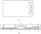
- the chip assembly 7 may include a single chip, or as shown in Fig. 8 , the chip assembly 7 may include a first chip 71 and a second chip 72, both of which are arranged in the region of the bent part 112 parallel to the substrate body 111, and are in conduction with the bent part 112, respectively.
- the first chip 71 and the second chip 72 Through the first chip 71 and the second chip 72, the related signals of the thin film transistor layer of the display screen 1 can be collected and further output through the flexible circuit board 6.
- arranging two chips can reduce the requirements on the processing resources of the chips.
- at least one of the first chip 71 and the second chip 72 may be arranged in the second avoidance part 25 of the first support plate 2.
- the first chip 71 and the second chip 72 may be symmetrically arranged with respect to a center line of the bent part 112, and an extension direction of the center line is perpendicular to the first side surface (specifically, the edge of the first side surface), which is vertically arranged in Fig. 8 , so that the center line of the bent part 112 is horizontally arranged in Fig. 8 .
- the first chip 71 and the second chip 72 it is convenient for the signals output by the thin film transistor layer to be shunted by the two chips, and the electrical connection between the two chips and the bent part 112 can also be simplified.
- the electronic device 200 may be a device with the screen on a single side, or as shown in Fig. 9 , the electronic device 200 may be a foldable device.
- the electronic device 200 may also include a second support plate 9 and a rotating shaft 10, the second support plate 9 is connected to the second side surface of the substrate body 111 facing away from the display layer 12, the second support plate 9 is also connected to one side of the rotating shaft 10, and the first support plate 2 is connected to the other side of the rotating shaft 10. Subsequently, the second support plate 9 and the first support plate 2 can move close to each other or away from each other through the rotation of the rotating shaft 302, so that the electronic device 200 can be switched between a folded state and an unfolded state.
- the bent part 112 is bent to wrap the edge of the first side surface of the substrate body 111 adjacent to the first support plate 2, and the second support plate 9 is arranged in a flat shape.
- the related circuits of the array substrate 11 may also be led out from a side where the second support plate 9 is, and similarly, a bent part may also be provided.
- the subsequent battery arrangement and the subsequent related circuit board arrangement on the side corresponding to the second support plate 9 may refer to the previous embodiments, and will not be described in detail here.
Landscapes
- Engineering & Computer Science (AREA)
- Computer Hardware Design (AREA)
- Theoretical Computer Science (AREA)
- Physics & Mathematics (AREA)
- General Engineering & Computer Science (AREA)
- General Physics & Mathematics (AREA)
- Human Computer Interaction (AREA)
- Signal Processing (AREA)
- Microelectronics & Electronic Packaging (AREA)
- Mathematical Physics (AREA)
- Power Engineering (AREA)
- Telephone Set Structure (AREA)
- Structure Of Printed Boards (AREA)
- Mounting Of Printed Circuit Boards And The Like (AREA)
- Devices For Indicating Variable Information By Combining Individual Elements (AREA)
Applications Claiming Priority (1)
| Application Number | Priority Date | Filing Date | Title |
|---|---|---|---|
| CN202310187707.7A CN118553156A (zh) | 2023-02-24 | 2023-02-24 | 电子设备 |
Publications (1)
| Publication Number | Publication Date |
|---|---|
| EP4421588A1 true EP4421588A1 (fr) | 2024-08-28 |
Family
ID=87003240
Family Applications (1)
| Application Number | Title | Priority Date | Filing Date |
|---|---|---|---|
| EP23181617.4A Pending EP4421588A1 (fr) | 2023-02-24 | 2023-06-27 | Dispositif électronique avec une batterie à étages |
Country Status (5)
| Country | Link |
|---|---|
| US (1) | US12339710B2 (fr) |
| EP (1) | EP4421588A1 (fr) |
| JP (1) | JP7526319B1 (fr) |
| KR (1) | KR102884926B1 (fr) |
| CN (1) | CN118553156A (fr) |
Citations (8)
| Publication number | Priority date | Publication date | Assignee | Title |
|---|---|---|---|---|
| EP2547180A2 (fr) * | 2011-07-13 | 2013-01-16 | Samsung Electronics Co., Ltd. | Dispositif d'affichage à diode électroluminescente organique à matrice active de panneau d'écran tactile avec plaque de circuit imprimé flexible |
| US20170170255A1 (en) * | 2015-12-15 | 2017-06-15 | Samsung Display Co., Ltd. | Flexible display apparatus |
| WO2018057652A1 (fr) * | 2016-09-22 | 2018-03-29 | Apple Inc. | Module d'affichage et vitrage avec cadre en plastique à contre-dépouille |
| EP3306743A1 (fr) * | 2016-10-05 | 2018-04-11 | Samsung Electronics Co., Ltd. | Dispositif électronique doté d'une antenne en boucle |
| US20190369668A1 (en) * | 2018-06-01 | 2019-12-05 | Samsung Electronics Co., Ltd. | Electronic device including foldable display |
| WO2022015012A1 (fr) * | 2020-07-14 | 2022-01-20 | 삼성전자 주식회사 | Dispositif électronique comprenant un écran souple |
| US20220248534A1 (en) * | 2021-01-29 | 2022-08-04 | Chengdu Boe Optoelectronics Technology Co., Ltd. | Flexible display module and manufacturing method thereof |
| CN115083291A (zh) * | 2022-07-25 | 2022-09-20 | 京东方科技集团股份有限公司 | 显示面板和显示装置 |
Family Cites Families (13)
| Publication number | Priority date | Publication date | Assignee | Title |
|---|---|---|---|---|
| KR100440934B1 (ko) * | 2002-02-06 | 2004-07-21 | 삼성에스디아이 주식회사 | 이차전지 |
| KR102020982B1 (ko) * | 2013-02-28 | 2019-09-16 | 엘지디스플레이 주식회사 | 플렉서블 디스플레이 장치 및 그 제조 방법 |
| KR102046864B1 (ko) * | 2013-03-13 | 2019-11-20 | 삼성전자주식회사 | 유연성 디스플레이 장치 |
| KR102400871B1 (ko) * | 2015-07-31 | 2022-05-23 | 엘지디스플레이 주식회사 | 플렉서블 표시 장치 및 그의 제조 방법 |
| CN117666709A (zh) * | 2016-10-27 | 2024-03-08 | 株式会社半导体能源研究所 | 数据处理装置、显示装置以及电子设备 |
| KR102364470B1 (ko) * | 2017-08-23 | 2022-02-18 | 삼성전자주식회사 | 안테나를 포함하는 전자 장치 |
| KR102555984B1 (ko) * | 2018-07-27 | 2023-07-14 | 삼성디스플레이 주식회사 | 압력 센서를 갖는 표시 장치 |
| KR102703682B1 (ko) * | 2018-10-29 | 2024-09-04 | 엘지디스플레이 주식회사 | 플렉서블 회로 필름 및 이를 포함하는 전자 기기 |
| KR102804208B1 (ko) * | 2020-01-15 | 2025-05-09 | 삼성전자주식회사 | 안테나를 포함하는 디스플레이 조립체 및 이를 포함하는 전자 장치 |
| KR102400030B1 (ko) * | 2020-11-18 | 2022-05-18 | 동우 화인켐 주식회사 | 안테나 패키지 및 이를 포함하는 화상 표시 장치 |
| JP7638794B2 (ja) * | 2021-06-04 | 2025-03-04 | 株式会社ジャパンディスプレイ | 表示装置 |
| CN113471240B (zh) * | 2021-06-30 | 2024-09-20 | 上海天马微电子有限公司 | 发光模组及其制备方法、显示装置 |
| CN115202502A (zh) * | 2022-06-10 | 2022-10-18 | 昆山国显光电有限公司 | 显示模组及显示模组的制造方法 |
-
2023
- 2023-02-24 CN CN202310187707.7A patent/CN118553156A/zh active Pending
- 2023-06-21 KR KR1020230079584A patent/KR102884926B1/ko active Active
- 2023-06-23 US US18/213,731 patent/US12339710B2/en active Active
- 2023-06-27 EP EP23181617.4A patent/EP4421588A1/fr active Pending
- 2023-06-29 JP JP2023106913A patent/JP7526319B1/ja active Active
Patent Citations (9)
| Publication number | Priority date | Publication date | Assignee | Title |
|---|---|---|---|---|
| EP2547180A2 (fr) * | 2011-07-13 | 2013-01-16 | Samsung Electronics Co., Ltd. | Dispositif d'affichage à diode électroluminescente organique à matrice active de panneau d'écran tactile avec plaque de circuit imprimé flexible |
| US20170170255A1 (en) * | 2015-12-15 | 2017-06-15 | Samsung Display Co., Ltd. | Flexible display apparatus |
| WO2018057652A1 (fr) * | 2016-09-22 | 2018-03-29 | Apple Inc. | Module d'affichage et vitrage avec cadre en plastique à contre-dépouille |
| EP3306743A1 (fr) * | 2016-10-05 | 2018-04-11 | Samsung Electronics Co., Ltd. | Dispositif électronique doté d'une antenne en boucle |
| US20190369668A1 (en) * | 2018-06-01 | 2019-12-05 | Samsung Electronics Co., Ltd. | Electronic device including foldable display |
| WO2022015012A1 (fr) * | 2020-07-14 | 2022-01-20 | 삼성전자 주식회사 | Dispositif électronique comprenant un écran souple |
| EP4170454A1 (fr) * | 2020-07-14 | 2023-04-26 | Samsung Electronics Co., Ltd. | Dispositif électronique comprenant un écran souple |
| US20220248534A1 (en) * | 2021-01-29 | 2022-08-04 | Chengdu Boe Optoelectronics Technology Co., Ltd. | Flexible display module and manufacturing method thereof |
| CN115083291A (zh) * | 2022-07-25 | 2022-09-20 | 京东方科技集团股份有限公司 | 显示面板和显示装置 |
Also Published As
| Publication number | Publication date |
|---|---|
| JP7526319B1 (ja) | 2024-07-31 |
| CN118553156A (zh) | 2024-08-27 |
| KR20240131865A (ko) | 2024-09-02 |
| US20240288908A1 (en) | 2024-08-29 |
| JP2024120824A (ja) | 2024-09-05 |
| US12339710B2 (en) | 2025-06-24 |
| KR102884926B1 (ko) | 2025-11-12 |
Similar Documents
| Publication | Publication Date | Title |
|---|---|---|
| JP5067662B2 (ja) | 装着可能な集積回路パッケージインパッケージシステムおよびその製造方法 | |
| US8634204B2 (en) | Compact folded configuration for integrated circuit packaging | |
| KR20140080136A (ko) | 반도체 패키지 | |
| JP2009259207A (ja) | 半導体メモリカードとそれに用いられる半導体メモリデバイス | |
| CN107577278A (zh) | 一种显示屏组件及移动终端 | |
| US12339709B2 (en) | Electronic device | |
| KR20150049166A (ko) | 반도체 패키지 | |
| CN112153845B (zh) | 电子设备及其电路模组 | |
| EP3993387A1 (fr) | Base, module de caméra et dispositif électronique | |
| EP4421588A1 (fr) | Dispositif électronique avec une batterie à étages | |
| JP3138127U (ja) | メモリカード | |
| US20060138630A1 (en) | Stacked ball grid array packages | |
| CN213693794U (zh) | 显示屏组件及移动终端 | |
| CN110636701A (zh) | 电路板装置及电子设备 | |
| US20220294941A1 (en) | Base, camera module and electronic device | |
| US12339708B2 (en) | Electronic device | |
| CN110188677B (zh) | 指纹模组及移动终端 | |
| CN212365016U (zh) | 防水侧边指纹装置及终端 | |
| CN118629323A (zh) | 显示屏和电子设备 | |
| CN119744090A (zh) | 显示模组、电子设备及显示模组的制备方法 | |
| CN116896824A (zh) | 电池保护板模组、方法、装置、电池模组以及电子设备 | |
| KR100861255B1 (ko) | 분할형 연결단자를 구비한 연성회로기판을 포함한휴대단말기 | |
| JP2006114533A (ja) | 半導体装置 | |
| JP2008205320A (ja) | 半導体装置 | |
| JP2007012348A (ja) | メモリカード用コネクタ及びこれを用いた携帯電話機 |
Legal Events
| Date | Code | Title | Description |
|---|---|---|---|
| PUAI | Public reference made under article 153(3) epc to a published international application that has entered the european phase |
Free format text: ORIGINAL CODE: 0009012 |
|
| STAA | Information on the status of an ep patent application or granted ep patent |
Free format text: STATUS: THE APPLICATION HAS BEEN PUBLISHED |
|
| AK | Designated contracting states |
Kind code of ref document: A1 Designated state(s): AL AT BE BG CH CY CZ DE DK EE ES FI FR GB GR HR HU IE IS IT LI LT LU LV MC ME MK MT NL NO PL PT RO RS SE SI SK SM TR |
|
| STAA | Information on the status of an ep patent application or granted ep patent |
Free format text: STATUS: REQUEST FOR EXAMINATION WAS MADE |
|
| 17P | Request for examination filed |
Effective date: 20250228 |