EP4421992A1 - Antennenzelle mit sendernetzwerk - Google Patents
Antennenzelle mit sendernetzwerk Download PDFInfo
- Publication number
- EP4421992A1 EP4421992A1 EP24157412.8A EP24157412A EP4421992A1 EP 4421992 A1 EP4421992 A1 EP 4421992A1 EP 24157412 A EP24157412 A EP 24157412A EP 4421992 A1 EP4421992 A1 EP 4421992A1
- Authority
- EP
- European Patent Office
- Prior art keywords
- antenna element
- cell
- antenna
- phase shift
- circuit
- Prior art date
- Legal status (The legal status is an assumption and is not a legal conclusion. Google has not performed a legal analysis and makes no representation as to the accuracy of the status listed.)
- Pending
Links
Images


Classifications
-
- H—ELECTRICITY
- H01—ELECTRIC ELEMENTS
- H01Q—ANTENNAS, i.e. RADIO AERIALS
- H01Q3/00—Arrangements for changing or varying the orientation or the shape of the directional pattern of the waves radiated from an antenna or antenna system
- H01Q3/44—Arrangements for changing or varying the orientation or the shape of the directional pattern of the waves radiated from an antenna or antenna system varying the electric or magnetic characteristics of reflecting, refracting, or diffracting devices associated with the radiating element
- H01Q3/46—Active lenses or reflecting arrays
-
- H—ELECTRICITY
- H04—ELECTRIC COMMUNICATION TECHNIQUE
- H04B—TRANSMISSION
- H04B1/00—Details of transmission systems, not covered by a single one of groups H04B3/00 - H04B13/00; Details of transmission systems not characterised by the medium used for transmission
- H04B1/38—Transceivers, i.e. devices in which transmitter and receiver form a structural unit and in which at least one part is used for functions of transmitting and receiving
-
- H—ELECTRICITY
- H01—ELECTRIC ELEMENTS
- H01Q—ANTENNAS, i.e. RADIO AERIALS
- H01Q21/00—Antenna arrays or systems
- H01Q21/0006—Particular feeding systems
- H01Q21/0018—Space- fed arrays
-
- H—ELECTRICITY
- H01—ELECTRIC ELEMENTS
- H01Q—ANTENNAS, i.e. RADIO AERIALS
- H01Q21/00—Antenna arrays or systems
- H01Q21/24—Combinations of antenna units polarised in different directions for transmitting or receiving circularly and elliptically polarised waves or waves linearly polarised in any direction
-
- H—ELECTRICITY
- H01—ELECTRIC ELEMENTS
- H01Q—ANTENNAS, i.e. RADIO AERIALS
- H01Q3/00—Arrangements for changing or varying the orientation or the shape of the directional pattern of the waves radiated from an antenna or antenna system
- H01Q3/26—Arrangements for changing or varying the orientation or the shape of the directional pattern of the waves radiated from an antenna or antenna system varying the relative phase or relative amplitude of energisation between two or more active radiating elements; varying the distribution of energy across a radiating aperture
- H01Q3/30—Arrangements for changing or varying the orientation or the shape of the directional pattern of the waves radiated from an antenna or antenna system varying the relative phase or relative amplitude of energisation between two or more active radiating elements; varying the distribution of energy across a radiating aperture varying the relative phase between the radiating elements of an array
- H01Q3/34—Arrangements for changing or varying the orientation or the shape of the directional pattern of the waves radiated from an antenna or antenna system varying the relative phase or relative amplitude of energisation between two or more active radiating elements; varying the distribution of energy across a radiating aperture varying the relative phase between the radiating elements of an array by electrical means
- H01Q3/36—Arrangements for changing or varying the orientation or the shape of the directional pattern of the waves radiated from an antenna or antenna system varying the relative phase or relative amplitude of energisation between two or more active radiating elements; varying the distribution of energy across a radiating aperture varying the relative phase between the radiating elements of an array by electrical means with variable phase-shifters
-
- H—ELECTRICITY
- H04—ELECTRIC COMMUNICATION TECHNIQUE
- H04B—TRANSMISSION
- H04B1/00—Details of transmission systems, not covered by a single one of groups H04B3/00 - H04B13/00; Details of transmission systems not characterised by the medium used for transmission
- H04B1/02—Transmitters
- H04B1/04—Circuits
- H04B2001/0408—Circuits with power amplifiers
-
- H—ELECTRICITY
- H04—ELECTRIC COMMUNICATION TECHNIQUE
- H04B—TRANSMISSION
- H04B1/00—Details of transmission systems, not covered by a single one of groups H04B3/00 - H04B13/00; Details of transmission systems not characterised by the medium used for transmission
- H04B1/38—Transceivers, i.e. devices in which transmitter and receiver form a structural unit and in which at least one part is used for functions of transmitting and receiving
- H04B1/3805—Transceivers, i.e. devices in which transmitter and receiver form a structural unit and in which at least one part is used for functions of transmitting and receiving with built-in auxiliary receivers
- H04B2001/3811—Split configuration of transmission devices
Definitions
- This description relates generally to electronic devices and, more particularly, to the field of transmitarray radio antennas.
- radio antennas known as "transmitter array” antennas are known in particular. These antennas generally comprise several elementary cells each comprising a first antenna element irradiated by an electromagnetic field emitted by one or more sources, a second antenna element transmitting a modified signal to the outside of the antenna, and a coupling element between the first and second antenna elements.
- transceiver array antennas suitable for implementing simultaneous two-way communication.
- the transmission channel is adapted to transmit a first signal having a first polarization state
- the reception channel is adapted to receive a second signal having a second polarization state, different from the first polarization state.
- the first and second signals have orthogonal linear polarizations.
- the first and second signals have circular and linear polarizations, respectively.
- each of the first and second antenna elements comprises a substantially square-shaped conductive plane and first and second ports located respectively in the vicinity of first and second adjacent sides of the conductive plane.
- the first and second ports of the first antenna element are located respectively directly above the first and second ports of the second antenna element.
- the first and second ports of the first antenna element are respectively connected, by the first and second phase shift and amplification circuits, to the first and second ports of the second antenna element.
- the first and second ports of the first antenna element are respectively connected, by the first and second phase shift and amplification circuits, to the second and first ports of the second antenna element.
- the cell further comprises first and second ground planes interposed between the first antenna element and the second antenna element.
- the first and second phase shift and amplification circuits are interposed between the first and second ground planes.
- the first and second antenna elements and the first and second ground planes are formed in conductive levels of a printed circuit board.
- the transmit and receive channels each comprise a phase shift circuit and an amplification circuit connected in series between the first antenna element and the second antenna element.
- One embodiment provides a transmitter network comprising a plurality of cells as described.
- the first antenna element of each cell is electrically isolated from the first antenna element of each of the other cells
- the second antenna element of each cell is electrically isolated from the second antenna element of each of the other cells.
- One embodiment provides an antenna comprising a transmitter array as described and at least one source configured to irradiate a face of the array.
- each primary source is adapted to produce a generally conical beam irradiating all or part of the transmitting array.
- Each primary source comprises for example a horn antenna.
- the central axis of each primary source is substantially orthogonal to the mean plane of the array.
- the expressions “approximately”, “approximately”, “substantially”, and “of the order of” mean to within 10%, preferably to within 5%.
- FIG. 1 is a schematic and partial side view of an exemplary transmitarray antenna 100 of the type to which exemplary embodiments described apply.
- the antenna 100 typically comprises one or more primary sources 101 (a single source 101, in the example shown) irradiating a transmitting network 103.
- the source 101 may have any polarization, for example linear or circular.
- the network 103 comprises a plurality of elementary cells 105, for example arranged in a matrix according to rows and columns. Each cell 105 typically comprises a first antenna element 105a, located on the side of a first face of the network 103 arranged opposite the primary source 101, and a second antenna element 105b, located on the side of a second face of the network opposite the first face.
- the second face of the network 103 is for example turned towards a transmission medium, or external medium, of the antenna 100.
- Each cell 105 is capable, in transmission, of receiving electromagnetic radiation on its first antenna element 105a and of re-emitting this radiation from its second antenna element 105b, for example by introducing a known phase shift ⁇ .
- each cell 105 is capable of receiving electromagnetic radiation on its second antenna element 105b and of re-emitting this radiation from its first antenna element 105a, in the direction of the source 101, with the same phase shift ⁇ .
- the radiation re-emitted by the first antenna element 105a is for example focused on the source 101.
- the characteristics of the near-field or far-field radiation produced by the antenna 100 in particular its shape (or size), its intensity and its maximum emission direction (or pointing direction), depend on the values of the phase shifts respectively introduced by the different cells 105 of the network 103.
- transmitting array antennas are energy efficient and relatively simple, inexpensive and space-saving. This is due in particular to the fact that the transmitting arrays can be produced using planar technology, usually on printed circuit boards.
- the present description relates more particularly to antennas with a reconfigurable transmitter array 103.
- the transmitter array 103 is said to be reconfigurable when the elementary cells 105 are electronically controllable individually to modify their phase shift value ⁇ and/or their amplitude, which makes it possible to dynamically modify the characteristics of the radiation generated by the antenna, and in particular to modify its pointing direction without mechanically moving the antenna or a part of the antenna by means of a motorized element.
- FIG 2 is a schematic and partial side view of an exemplary antenna 200 with a transmitting array according to one embodiment.
- the antenna 200 of the figure 2 includes common elements with the 100 antenna of the figure 1 . These common elements will not be detailed again below.
- each elementary cell 105 of the transmitter network 103 comprises a transmission channel 201a and a reception channel 201b intended respectively to transmit and receive signals, for example simultaneously.
- each channel 201a, 201b connects the first antenna element 105a to the second antenna element 105b of the cell.
- the first antenna element 105a connects a first end of the transmission channel 201a to a first end of the reception channel 201b.
- the second antenna element 105b of the cell 105 connects a second end of the transmission channel 201a, opposite the first end of the channel 201a, to a second end of the reception channel 201b, opposite the first end of the channel 201b.
- first antenna element 105a of each elementary cell 105 is electrically isolated from the first antenna element 105a of each of the other cells 105
- second antenna element 105b of each elementary cell 105 is electrically isolated from the second antenna element 105b of each of the other cells 105.
- Each transmit channel 201a comprises a phase shift and amplification circuit 203a
- each receive channel 201b comprises a phase shift and amplification circuit 203b.
- each phase shift and amplification circuit 203a, 203b comprises, between the first and second antenna elements 105a and 105b, a phase shift circuit 205a, 205b associated in series with an amplification circuit 207a, 207b.
- the phase shift circuit 205a of the transmission channel 201a comprises a terminal connected, preferably connected, to the first antenna element 105a and another terminal connected, preferably connected, to a terminal, for example an input terminal, of the amplification circuit 207a, the amplification circuit 207a further comprising another terminal, for example an output terminal, connected, preferably connected, to the second antenna element 105b.
- the amplification circuit 270b of the reception channel 201b comprises a terminal, for example an input terminal, connected, preferably connected, to the second antenna element 105b and another terminal, for example an output terminal, connected, preferably connected, to a terminal of the phase shift circuit 205b, the phase shift circuit 205b further comprising another terminal connected, preferably connected, to the first antenna element 105a.
- each phase shift circuit 205a, 205b comprises at least one element selected from a diode, for example a PIN diode, a microelectromechanical system, a varicap or varactor diode, a phase shift integrated circuit, etc.
- Each phase shift circuit 205a, 205b receives for example a control signal coming from a control circuit (not illustrated in figure 2 ), for example a microcontroller, adapted to switch the signals transmitted by each circuit 205a, 205b between two distinct phase states.
- the amplification circuit 207a of the transmission channel 201a is for example a power amplifier, for example a linear class A amplifier in CMOS (Complementary Metal-Oxide-Semiconductor) SOI (Silicon On Insulator) technology. insulator), for example of the type described in the article by A. Hamani, A. Siligaris, B. Blampey and J. L. G. Jimenez entitled “167-GHz and 155-GHz High Gain D-band Power Amplifiers in CMOS SOI 45-nm Technology” from the fifteenth European Microwave Integrated Circuits Conference (EuMIC) in Utrecht, Netherlands 2021, pages 261–264 .
- CMOS Complementary Metal-Oxide-Semiconductor
- SOI Silicon On Insulator
- insulator for example of the type described in the article by A. Hamani, A. Siligaris, B. Blampey and J. L. G. Jimenez entitled “167-GHz and 155-
- the amplification circuit 207b of the reception channel 201b is for example a low noise amplifier (LNA). This makes it possible to optimize a noise figure of the reception channel 201b.
- LNA low noise amplifier
- each amplification circuit 207b comprises a class “AB” amplifier comprising for example one or two operating stages.
- Each amplification circuit 207b has for example an electrical power of between 10 and 20 mW.
- the source 101 of the transmitting array antenna 200 is connected to an interference elimination or cancellation circuit 211. More specifically, in this example, first and second links 213a and 213b, electrically isolated from each other, connect the circuit 211 to the source 101.
- the antenna 200 further comprises a processing circuit 215 connected to the circuit 211.
- the circuit 215 is connected to the circuit 211 by a transmission channel 217a comprising a digital-to-analog converter 219a associated in series with a mixer 221a (x).
- the circuit 211 is further connected to the circuit 215 by a reception channel 217b comprising a mixer 221b (x) associated in series with an analog-to-digital converter 219b.
- Each mixer 221a, 221b is for example connected to an oscillator 223a, 223b ( ⁇ ), for example a voltage controlled oscillator (VCO, in English) or a phase-locked loop (PLL).
- VCO voltage controlled oscillator
- PLL phase-locked loop
- the digital-to-analog converter 219a of the transmission channel 217a comprises input and output terminals connected respectively to the circuit 215 and to a terminal of the mixer 221a, the mixer 221a further comprising another terminal connected to the circuit 211.
- the mixer 221b of the reception channel 217b comprises a terminal connected to the circuit 211 and another terminal connected to an analog-to-digital converter input terminal 219b, the analog-to-digital converter 219b further comprising an output terminal connected to the circuit 215.
- circuit 215 is adapted to encode and modulate a signal to be transmitted by transmission channel 217a, and to demodulate and decode a signal received by reception channel 217b.
- the antenna 200 is configured to implement simultaneous bidirectional communication (“full-duplex” in English), that is to say that the antenna 200 can transmit and receive signals simultaneously in the same frequency band (“In-Band Full-Duplex” - IBFD, in English).
- the antenna 200 is notably different from frequency division multiple access antennas (“Frequency Division Multiple Access” - FDMA, in English) whose transmission and reception channels are separated in frequency.
- a first signal to be transmitted is for example produced by the circuit 215 then transmitted, via the transmission channel 217a and the first link 213a, to the source 101 irradiating the network 103.
- the first signal then reaches the first antenna elements 105a of the cells 105 of the network 103 then is transmitted, via the transmission channels 201a, to the second antenna elements 105b. to be radiated towards the external environment.
- a second signal to be received from the external environment is for example picked up by the second antenna elements 105b of the cells 105 of the network 103 and is then transmitted, via the reception channels 201b, to the first antenna elements 105a.
- the second signal is then radiated towards the source 101 and is then transmitted, via the second link 213b and the reception channel 217b, to the circuit 215 to be processed.
- the first antenna element 105a receives the signal radiated by the antenna 101.
- the signal is then phase-shifted and amplified by the transmission channel 201a, more precisely by the phase-shifting circuit 205a and by the amplification circuit 207a, respectively, then re-transmitted by the second antenna element 105b to the external environment.
- the second antenna element 105b receives the signal from the external environment.
- the signal is then amplified and then phase-shifted by the reception channel 201b, more precisely by the amplification circuit 207b and by the phase-shifting circuit 205b, respectively, then re-transmitted by the first antenna element to the source 101.
- the signals transmitted and received by the antenna 200 respectively have first and second distinct polarization states or directions.
- the signals transmitted and received respectively have first and second linear polarizations orthogonal to each other, the first polarization being for example a linear polarization called “vertical” and the second polarization a linear polarization called “horizontal”.
- the first and second polarizations may be a circular polarization.
- the first and second polarizations may be circular polarizations of opposite directions, the first polarization being for example a circular polarization called "left" (counterclockwise, from the point of view of the source 101) and the second polarization being for example a circular polarization called "right” (clockwise, from the point of view of the source 101), or the first polarization being a circular polarization and the second polarization being a linear polarization.
- the source 101 is for example a so-called "bipolarization" source, capable of emitting and receiving signals having two distinct polarizations respectively.
- the source 101 can be replaced by first and second spatially separated sources, the first source being for example adapted to emit signals having a first polarization and the second source being adapted to receive signals having a second polarization, different from the first polarization.
- the circuit 211 is connected to the first and second sources by the first and second links 213a and 213b, respectively.
- An advantage of the 200 antenna of the figure 2 is due to the fact that it allows for superior performance, particularly in terms of interference cancellation, to be achieved compared to existing antennas.
- FIG. 3A is a schematic and partial side view of the cell 105 of the transmitter network 103 according to one embodiment.
- the cell 105 comprises two disjoint ground planes M1 and M2 substantially parallel to each other and interposed between the first and second elements.
- antenna 105b The first and second antenna elements 105a and 105b are, in this example, substantially parallel to each other and to the ground planes M1 and M2.
- the circuits 203a and 203b are interposed between the ground planes M1 and M2.
- the phase shift and amplification circuit 203a is connected, by a conductive via V1a, to a first conduction port or terminal P1 of the first antenna element 105a.
- the circuit 203a is further connected, by another conductive via V2a, to a first conduction port or terminal P1 of the second antenna element 105b.
- the phase shift and amplification circuit 203b is connected, by a conductive via V2a, to a second conduction port or terminal P2 of the first antenna element 105a.
- the circuit 203b is further connected, by another conductive via V2b, to a second conduction port or terminal P2 of the second antenna element 105b.
- the first and second antenna elements 105a and 105b and the ground planes M1 and M2 are formed in conductive levels or metallization levels of a printed circuit board (PCB), the conductive levels being separated from each other by insulating levels not shown in FIG. Figure 3A .
- the circuits 203a and 203b are for example produced in CMOS or BiCMOS (Bipolar Complementary Metal Oxide Semiconductor) technology.
- the circuits 203a and 203b can be implemented in discrete or integrated components.
- an integrated circuit connected to several antennas can be provided.
- FIG. 3B is a schematic and partial top view of the first antenna element 105a of the cell 105 of the Figure 3A .
- the first antenna element 105a is a patch antenna comprising a substantially square-shaped conductive plane to which the vias V1a and V1b are connected by the ports P1 and P2, respectively.
- the conductive plane of the first antenna element 105a being able to have any shape, for example rectangular.
- the port P1 is located in the vicinity of a first side of the square formed by the conductive plane and the port P2 is located in the vicinity of a second side of the square adjacent to the first side.
- the ports P1 and P2 are substantially aligned with respect to the middles of the first and second sides, respectively.
- the first antenna element 105a is adapted to transmit, via the port P1, a first signal having a linear polarization (a horizontal polarization, in the orientation of the Figure 3B ).
- the first antenna element 105a is further adapted to transmit towards the source 101, from the port P2, a second signal having a linear polarization orthogonal to that of the first signal (a vertical polarization, in the orientation of the Figure 3B ).
- the second antenna element 105b is for example similar or identical to the first antenna element 105a.
- the ports P1 and P2 of the second antenna element 105b are located respectively in line with the ports P1 and P2 of the first antenna element 105a.
- the vias V2a and V2b are for example located respectively in line with the vias V1a and V1b.
- FIG. 3C is a schematic and partial top view of the ground plane M1 of cell 105 of the Figure 3A .
- vias V1a and V1b are electrically isolated from ground plane M1.
- vias V2a and V2b are, for example, electrically isolated from ground plane M2, ground plane M2 being, for example, analogous or identical to ground plane M1.
- FIG. 4A is a schematic and partial side view of the cell 105 according to another embodiment.
- the embodiment of the Figure 4A differs from that of the Figure 3A in that, in the embodiment of the Figure 4A , the first port P1 of the first antenna element 105a is connected to the second port P2 of the second antenna element 105b, and the second port P2 of the first antenna element 105a is connected to the first port P1 of the second antenna element 105b.
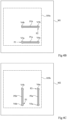
- FIG. 4B is a schematic and partial top view of the ground plane M1 of cell 105 of the Figure 4A and the Figure 4C is a schematic and partial top view of the ground plane M2 of cell 105 of the Figure 4A .
- the cell 105 may further comprise one or more redistribution layers (“Redistribution Layer” (RDL) of the transmitted and received radiofrequency signals, a ground signal and a power supply signal.
- RDL redistribution Layer
- tracks P1a and P1b are substantially parallel to each other, and tracks P2a and P2b are substantially parallel to each other and orthogonal to tracks P1a and P1b.
- An advantage of the embodiment of cell 105 set forth above in relation to the Figures 4A to 4C is that it allows to further reduce or cancel the interference between the signals transmitted and received by the antenna.
- the isolation of cell 105 from the Figures 4A to 4C is improved by a factor of two, in decibels (dB), compared to that of cell 105 of the Figures 3A to 3B .
- cell 105 detailed above in connection with the Figures 4A to 4C is not limited to the structure described, other cell structures 105 may be provided by the person skilled in the art, based on the indications of the present description, for connecting the ports P1 and P2 of the first antenna element 105a to the ports P2 and P1, respectively, of the second antenna element 105b.
- the person skilled in the art is able to adapt the structure of the cell 105, in particular of the first and second antenna elements 105a and 105b, in the event that the polarization of the signal to be transmitted and/or of the signal received by the antenna 200 has a polarization different from a linear polarization, for example a circular polarization.
Landscapes
- Engineering & Computer Science (AREA)
- Computer Networks & Wireless Communication (AREA)
- Signal Processing (AREA)
- Variable-Direction Aerials And Aerial Arrays (AREA)
Applications Claiming Priority (1)
| Application Number | Priority Date | Filing Date | Title |
|---|---|---|---|
| FR2301423A FR3145841B1 (fr) | 2023-02-15 | 2023-02-15 | Cellule d’antenne à réseau transmetteur |
Publications (1)
| Publication Number | Publication Date |
|---|---|
| EP4421992A1 true EP4421992A1 (de) | 2024-08-28 |
Family
ID=86764873
Family Applications (1)
| Application Number | Title | Priority Date | Filing Date |
|---|---|---|---|
| EP24157412.8A Pending EP4421992A1 (de) | 2023-02-15 | 2024-02-13 | Antennenzelle mit sendernetzwerk |
Country Status (3)
| Country | Link |
|---|---|
| US (1) | US20240275417A1 (de) |
| EP (1) | EP4421992A1 (de) |
| FR (1) | FR3145841B1 (de) |
Family Cites Families (2)
| Publication number | Priority date | Publication date | Assignee | Title |
|---|---|---|---|---|
| US9966989B2 (en) * | 2007-10-17 | 2018-05-08 | Applied Radar, Inc. | Array antenna system and spread spectrum beamformer method |
| US10735872B2 (en) * | 2018-08-09 | 2020-08-04 | Starkey Laboratories, Inc. | Hearing device incorporating phased array antenna arrangement |
-
2023
- 2023-02-15 FR FR2301423A patent/FR3145841B1/fr active Active
-
2024
- 2024-02-13 EP EP24157412.8A patent/EP4421992A1/de active Pending
- 2024-02-14 US US18/441,237 patent/US20240275417A1/en active Pending
Non-Patent Citations (7)
| Title |
|---|
| A. HAMANIA. SILIGARISB. BLAMPEYJ. L. G. JIMENEZ: "167-GHz and 155-GHz High Gain D-band Power Amplifiers in CMOS SOI 45-nm Technology", EUROPEAN MICROWAVE INTEGRATED CIRCUITS CONFÉRENCE (EUMIC) » À UTRECHT, PAYS-BAS, 2021, pages 261 - 264 |
| FORMAN M ET AL: "A K-band full-duplex transmit-receive lens array", 2001 IEEE MTT-S INTERNATIONAL MICROWAVE SYMPOSIUM DIGEST.(IMS 2001). PHOENIX, AZ, MAY 20 - 25, 2001; [IEEE MTT-S INTERNATIONAL MICROWAVE SYMPOSIUM], NEW YORK, NY : IEEE, US, 20 May 2001 (2001-05-20), pages 1831, XP032405872, ISBN: 978-0-7803-6538-4, DOI: 10.1109/MWSYM.2001.967263 * |
| LANDSBERG NAFTALI ET AL: "Design and Measurements of 100 GHz Reflectarray and Transmitarray Active Antenna Cells", IEEE TRANSACTIONS ON ANTENNAS AND PROPAGATION, IEEE, USA, vol. 65, no. 12, 5 October 2017 (2017-10-05), pages 6986 - 6997, XP011673503, ISSN: 0018-926X, [retrieved on 20171128], DOI: 10.1109/TAP.2017.2759840 * |
| ORTIZ S ET AL: "A compact circularly polarized microstrip transmit-receive antenna for LAN applications", ANTENNAS AND PROPAGATION SOCIETY INTERNATIONAL SYMPOSIUM, 1998. IEEE ATLANTA, GA, USA 21-26 JUNE 1998, NEW YORK, NY, USA,IEEE, US, 21 June 1998 (1998-06-21), pages 2104, XP032386314, ISBN: 978-0-7803-4478-5, DOI: 10.1109/APS.1998.701624 * |
| ORTIZ S ET AL: "A transmit-receive spatial amplifier array", MICROWAVE SYMPOSIUM DIGEST, 1997., IEEE MTT-S INTERNATIONAL DENVER, CO, USA 8-13 JUNE 1997, NEW YORK, NY, USA,IEEE, US, 8 June 1997 (1997-06-08), pages 679 - 682vol.2, XP032379800, ISBN: 978-0-7803-3814-2, DOI: 10.1109/MWSYM.1997.602882 * |
| PAN WENBO ET AL: "An Amplifying Tunable Transmitarray Element", IEEE ANTENNAS AND WIRELESS PROPAGATION LETTERS, vol. 13, 25 March 2014 (2014-03-25), pages 702 - 705, XP011545949, ISSN: 1536-1225, [retrieved on 20140418], DOI: 10.1109/LAWP.2014.2313596 * |
| POPOVIC Z ET AL: "QUASI-OPTICAL TRANSMIT/RECEIVE FRONT ENDS", IEEE TRANSACTIONS ON MICROWAVE THEORY AND TECHNIQUES, IEEE, USA, vol. 46, no. 11, PART 02, 1 November 1998 (1998-11-01), pages 1964 - 1974, XP000785386, ISSN: 0018-9480, DOI: 10.1109/22.734521 * |
Also Published As
| Publication number | Publication date |
|---|---|
| US20240275417A1 (en) | 2024-08-15 |
| FR3145841A1 (fr) | 2024-08-16 |
| FR3145841B1 (fr) | 2025-10-03 |
Similar Documents
| Publication | Publication Date | Title |
|---|---|---|
| EP4117117B1 (de) | Antennenzelle mit sendenetz | |
| EP3392959B1 (de) | Grundzelle eines übertragungsnetzes für eine rekonfigurierbare antenne | |
| CA2053643C (fr) | Dispositif d'alimentation d'un element rayonnant fonctionnant en double polarisation | |
| CA2110634C (fr) | Antenne active a synthese de polarisation variable | |
| EP0108463B1 (de) | Strahlelement für orthogonal polarisierte Signale und flache Antennengruppe mit solchen nebeneinandergestellten Elementen | |
| EP3577720B1 (de) | Elementare antenne mit einer planaren strahlungsvorrichtung | |
| FR2648626A1 (fr) | Element rayonnant diplexant | |
| EP2532046A1 (de) | Flachplatten-abtastantenne für landfahrzeuganwendung, fahrzeug mit einer solchen antenne und satellitentelekommunikationssystem mit solch einem fahrzeug | |
| FR2866480A1 (fr) | Dispositif rayonnant compact multipolarisation a alimentation orthogonale par ligne(s) a champ de surface | |
| EP3329550B1 (de) | Sender-empfänger und zugehörige antenne | |
| FR3079075A1 (fr) | Antenne a reseau transmetteur large bande | |
| EP3176875A1 (de) | Aufbau einer aktiven hybriden rekonfigurierbaren strahlbildungsantenne | |
| WO1999060661A1 (fr) | Dispositif d'emission et de reception d'ondes hyperfrequences polarisees circulairement | |
| EP0518271A1 (de) | Mikrowellen-Antennenelement mit zwei Polarisationen | |
| EP0295688A1 (de) | Mikrowellenprimärsende- und Empfangsduplexer für orthogonalpolarisierte Wellen | |
| EP4421992A1 (de) | Antennenzelle mit sendernetzwerk | |
| EP4560832A1 (de) | Antennenzelle mit sendernetzwerk | |
| EP4092831B1 (de) | Antenne mit lückenhaftem verteilungsnetz | |
| EP4087060A1 (de) | Antennenzelle mit sendernetz | |
| EP4535564B1 (de) | Rekonfigurierbare antenne | |
| EP4535565A1 (de) | Rekonfigurierbare antenne | |
| EP0638821B1 (de) | In einem Satelliten untergebrachtes Mikrowellen-Abbildungsradarsystem mit doppeltem Erfassungsbereich | |
| EP0993073A1 (de) | Platte mit aktiven Antennen mit einer Mehrschichtstruktur | |
| WO2025016823A1 (fr) | Cellule polarisante, reseau transmetteur et antennes d'emission et de reception radio | |
| WO1999060717A1 (fr) | Circuit et procede de reception ou d'emission d'ondes hyperfrequences |
Legal Events
| Date | Code | Title | Description |
|---|---|---|---|
| PUAI | Public reference made under article 153(3) epc to a published international application that has entered the european phase |
Free format text: ORIGINAL CODE: 0009012 |
|
| STAA | Information on the status of an ep patent application or granted ep patent |
Free format text: STATUS: REQUEST FOR EXAMINATION WAS MADE |
|
| 17P | Request for examination filed |
Effective date: 20240213 |
|
| AK | Designated contracting states |
Kind code of ref document: A1 Designated state(s): AL AT BE BG CH CY CZ DE DK EE ES FI FR GB GR HR HU IE IS IT LI LT LU LV MC ME MK MT NL NO PL PT RO RS SE SI SK SM TR |
|
| RAP3 | Party data changed (applicant data changed or rights of an application transferred) |
Owner name: COMMISSARIAT A L'ENERGIE ATOMIQUE ET AUX ENERGIESALTERNATIVES |