EP4421994A1 - Übertragungsleitungsverbindungsstruktur - Google Patents
Übertragungsleitungsverbindungsstruktur Download PDFInfo
- Publication number
- EP4421994A1 EP4421994A1 EP22906376.3A EP22906376A EP4421994A1 EP 4421994 A1 EP4421994 A1 EP 4421994A1 EP 22906376 A EP22906376 A EP 22906376A EP 4421994 A1 EP4421994 A1 EP 4421994A1
- Authority
- EP
- European Patent Office
- Prior art keywords
- connection structure
- coupling
- ground layer
- transmission line
- coupling section
- Prior art date
- Legal status (The legal status is an assumption and is not a legal conclusion. Google has not performed a legal analysis and makes no representation as to the accuracy of the status listed.)
- Pending
Links
- 230000005540 biological transmission Effects 0.000 title claims abstract description 185
- 238000010168 coupling process Methods 0.000 claims abstract description 408
- 238000005859 coupling reaction Methods 0.000 claims abstract description 408
- 230000008878 coupling Effects 0.000 claims abstract description 398
- 239000004020 conductor Substances 0.000 claims abstract description 128
- 238000009413 insulation Methods 0.000 claims description 26
- 238000010586 diagram Methods 0.000 description 19
- 230000007704 transition Effects 0.000 description 12
- 230000008054 signal transmission Effects 0.000 description 11
- 239000002184 metal Substances 0.000 description 6
- 230000007423 decrease Effects 0.000 description 5
- 230000003071 parasitic effect Effects 0.000 description 4
- 230000008859 change Effects 0.000 description 3
- 238000002955 isolation Methods 0.000 description 3
- 230000009471 action Effects 0.000 description 2
- 230000001154 acute effect Effects 0.000 description 2
- 239000000463 material Substances 0.000 description 2
- 238000000034 method Methods 0.000 description 1
- 230000035515 penetration Effects 0.000 description 1
- 230000008569 process Effects 0.000 description 1
- 230000005855 radiation Effects 0.000 description 1
- 230000035945 sensitivity Effects 0.000 description 1
Images





Classifications
-
- H—ELECTRICITY
- H01—ELECTRIC ELEMENTS
- H01Q—ANTENNAS, i.e. RADIO AERIALS
- H01Q13/00—Waveguide horns or mouths; Slot antennas; Leaky-waveguide antennas; Equivalent structures causing radiation along the transmission path of a guided wave
- H01Q13/08—Radiating ends of two-conductor microwave transmission lines, e.g. of coaxial lines, of microstrip lines
-
- H—ELECTRICITY
- H01—ELECTRIC ELEMENTS
- H01P—WAVEGUIDES; RESONATORS, LINES, OR OTHER DEVICES OF THE WAVEGUIDE TYPE
- H01P3/00—Waveguides; Transmission lines of the waveguide type
- H01P3/02—Waveguides; Transmission lines of the waveguide type with two longitudinal conductors
- H01P3/08—Microstrips; Strip lines
-
- H—ELECTRICITY
- H01—ELECTRIC ELEMENTS
- H01P—WAVEGUIDES; RESONATORS, LINES, OR OTHER DEVICES OF THE WAVEGUIDE TYPE
- H01P5/00—Coupling devices of the waveguide type
- H01P5/08—Coupling devices of the waveguide type for linking dissimilar lines or devices
-
- H—ELECTRICITY
- H01—ELECTRIC ELEMENTS
- H01P—WAVEGUIDES; RESONATORS, LINES, OR OTHER DEVICES OF THE WAVEGUIDE TYPE
- H01P5/00—Coupling devices of the waveguide type
- H01P5/02—Coupling devices of the waveguide type with invariable factor of coupling
-
- H—ELECTRICITY
- H01—ELECTRIC ELEMENTS
- H01Q—ANTENNAS, i.e. RADIO AERIALS
- H01Q1/00—Details of, or arrangements associated with, antennas
- H01Q1/48—Earthing means; Earth screens; Counterpoises
-
- H—ELECTRICITY
- H01—ELECTRIC ELEMENTS
- H01Q—ANTENNAS, i.e. RADIO AERIALS
- H01Q1/00—Details of, or arrangements associated with, antennas
- H01Q1/12—Supports; Mounting means
- H01Q1/22—Supports; Mounting means by structural association with other equipment or articles
- H01Q1/24—Supports; Mounting means by structural association with other equipment or articles with receiving set
- H01Q1/241—Supports; Mounting means by structural association with other equipment or articles with receiving set used in mobile communications, e.g. GSM
- H01Q1/246—Supports; Mounting means by structural association with other equipment or articles with receiving set used in mobile communications, e.g. GSM specially adapted for base stations
Definitions
- Embodiments of this application relate to the antenna field, and in particular, to a transmission line connection structure.
- An antenna feed network of a base station includes transmission lines in different forms, and a transfer location exists between the different transmission lines. Due to field discontinuity, a severe loss occurs on the transfer location between the different transmission lines in a signal transmission process. This severely affects antenna system efficiency, a pattern gain, and the like. For example, in a feed network, a transfer location between a microstrip and a stripline causes a severe loss, and even excites a parasitic resonance mode. This severely affects signal transmission.
- a ground rod structure is added at a transfer location, and impact of field transfer discontinuity is reduced by using a ground screw or a metalized via, so that a transmission loss is reduced.
- this manner usually affects transmission line matching, increases a standing wave ratio, and use of the screw may cause a passive intermodulation risk. Therefore, how to better reduce impact caused by field discontinuity and obtain a better transfer apparatus to transit transmission lines in different forms becomes an urgent problem to be resolved.
- Embodiments of this application provide a transmission line connection structure. At a transfer location between two transmission lines, discontinuous ground layers are connected by using a coupling connection structure, to reduce a transmission loss caused by field discontinuity.
- a first aspect of embodiments of this application provides a transmission line connection structure.
- the transmission line connection structure includes as follows.
- the transmission line connection structure includes a first transmission line, a second transmission line, and a coupling connection structure.
- the first transmission line includes a conductor strip and a first ground layer
- the second transmission line includes the conductor strip and a second ground layer. Because the first ground layer and the second ground layer are discontinuous, a large loss usually occurs on a transfer location between a first transmission line and a second transmission line.
- the coupling connection structure is located near the conductor strip at the transfer location, and is configured to be coupled to the first ground layer and the second ground layer, to reduce impact caused by field discontinuity.
- the coupling connection structure includes a first coupling section 101, a second coupling section 102, and a third coupling section 103.
- a conductor part of the first coupling section 101 is coupled to the first ground layer
- a conductor part of the third coupling section 103 is coupled to the second ground layer
- the second coupling section 102 is connected to the first coupling section 101 and the third coupling section 103.
- the coupling connection structure is used as a transition structure near the transfer location between the first transmission line and the second transmission line, so that a loss caused by the field discontinuity can be greatly reduced, a parasitic resonance mode in an operating frequency band can be fully suppressed, and a transmission loss can be reduced.
- a location of the coupling connection structure may be more flexibly adjusted, so that transmission line impedance matching is properly controlled.
- a passive intermodulation risk can be avoided by using the coupling connection structure. Therefore, the transmission line connection structure has better performance, and transmission efficiency can be improved when signal transmission is performed between different transmission lines.
- the first coupling section 101 and the third coupling section 103 in the coupling connection structure are on different horizontal planes, and the first coupling section 101 is parallel to the third coupling section 103.
- the second coupling section 102 is perpendicular to the first coupling section 101 and the third coupling section 103. Because the second coupling section 102 is perpendicular to the first coupling section 101 and the third coupling section 103, a volume of the coupling connection structure 401 is small. This is more conducive to arrangement of the coupling connection structure 401 at a transfer location between different transmission lines.
- the first coupling section 101 and the third coupling section 103 in the coupling connection structure are on different horizontal planes, and the first coupling section 101 is parallel to the third coupling section 103.
- the second coupling section 102 is tilted relative to the first coupling section 101, and a tilt angle is formed between the second coupling section 102 and the first ground layer.
- the location of the coupling connection structure may be adjusted to control the transmission line impedance matching
- tilt of the coupling transition structure may be adjusted to control the transmission line impedance matching.
- the tilt angle of the coupling transition structure decreases, so that a field change becomes smoother. This can further reduce the loss.
- impact on the impedance matching is also reduced, and a voltage standing wave ratio decreases constantly.
- the conductor strip may have a coupling connection structure on one side, or may have a coupling connection structure on each of two sides.
- the transmission line connection structure may include a first coupling connection structure and a second coupling connection structure.
- the first coupling connection structure is located on a first side of the conductor strip
- the second coupling connection structure is located on a second side of the conductor strip.
- the first coupling connection structure and the second coupling connection structure may be symmetrically distributed on both sides of the conductor strip, to further reduce the loss caused by the field discontinuity.
- a plurality of coupling connection structures on both sides of the conductor strip may share a part of the coupling sections.
- the first coupling connection structure and the second coupling connection structure may share the third coupling section 103 coupled to the second ground layer. In this way, the first coupling connection structure and the second coupling connection structure may bypass the conductor strip and are bridged between the first ground layer and the second ground layer by.
- the coupling connection structure may be a multi-coupling connection structure.
- the coupling connection structure may include a third coupling connection structure, a fourth coupling connection structure, a fifth coupling connection structure, and a sixth coupling connection structure.
- the third coupling connection structure is located on a first side of a first section of the conductor strip
- the fourth coupling connection structure is located on a second side of the first section of the conductor strip
- the fifth coupling connection structure is located on a first side of a second section of the conductor strip
- the sixth coupling connection structure is located on a second side of the second section of the conductor strip.
- Each section of the conductor strip has a coupling connection structure on each of two sides, to reduce a loss.
- the third coupling connection structure and the fourth coupling connection structure may share one third coupling section 103 coupled to the second ground layer
- the fourth coupling connection structure and the fifth coupling connection structure may share one first coupling section 101 coupled to the first ground layer
- the fifth coupling connection structure and the sixth coupling connection structure may share one third coupling section 103 coupled to the second ground layer.
- the coupling connection structure includes the conductor part and an insulation part.
- the insulation medium part exists between the first coupling section 101 and the first ground layer, and the insulation medium part exists between the third coupling section 103 and the second ground layer.
- the second coupling section 102 may have an insulation medium part, or may not have an insulation medium part. This is not specifically limited.
- a second aspect of embodiments of this application provides another transmission line connection structure.
- the transmission line connection structure includes as follows.
- the transmission line connection structure includes a first transmission line, a second transmission line, a third transmission line, a fourth transmission line, and a coupling connection structure.
- the transmission line connection structure includes two conductor strips. A first conductor strip and a first ground layer correspond to the first transmission line. The first conductor strip and a second ground layer correspond to the second transmission line. A second conductor strip and the first ground layer correspond to the third transmission line. The second conductor strip and a third ground layer correspond to the fourth transmission line.
- the first ground layer, the second ground layer, and the third ground layer are all discontinuous.
- the coupling connection structure is configured to be bridged between the first ground layer, the second ground layer, and the third ground layer, and includes a first coupling section 101, a second coupling section 102, a third coupling section 103, a fourth coupling section 104, and a fifth coupling section 105.
- a conductor part of the first coupling section 101 is coupled to the first ground layer
- a conductor part of the third coupling section 103 is coupled to the second ground layer
- the second coupling section 102 is connected to the first coupling section 101 and the third coupling section 103.
- a conductor part of the fifth coupling section 105 is coupled to the third ground layer
- the fourth coupling section 104 is connected to the first coupling section 101 and the fifth coupling section 105.
- the coupling connection structure is configured to be coupled to the first ground layer and the second ground layer, and be coupled to the first ground layer and the third ground layer.
- the coupling connection structure is used, to reduce impact of field transfer discontinuity and ground layer discontinuity, and greatly reduce a loss.
- a location of the coupling connection structure may be more flexibly adjusted, so that transmission line impedance matching is properly controlled.
- a passive intermodulation risk can be avoided by using the coupling connection structure and isolation between two lines can be improved. Therefore, the transmission line connection structure has better performance, and transmission efficiency is further improved when signal transmission is performed between different transmission lines.
- the coupling connection structure includes the conductor part and an insulation part.
- the insulation medium part exists between the first coupling section 101 and the first ground layer, the insulation medium part exists between the third coupling section 103 and the second ground layer, and the insulation medium part exists between the fifth coupling section 105 and the third ground layer.
- the second coupling section 102 and the fourth coupling section 104 may have insulation medium parts, or may not have insulation medium parts. This is not specifically limited.
- Embodiments of this application provide a transmission line connection structure. At a transfer location between two transmission lines, discontinuous ground layers are connected by using a coupling connection structure, to reduce a transmission loss caused by field discontinuity.
- FIG. 1 is a diagram of a structure of a base station antenna feeder system according to an embodiment of this application.
- the base station antenna feeder system includes a base station antenna, a pole, an antenna adjustment support, a ground apparatus, and the like.
- a diagram of a structure of the base station antenna is shown in FIG. 2 .
- the base station antenna includes radiating elements, a metal reflection plate, a transmission or calibration network, a feed network, a radome, and the like.
- the radiating element is also referred to as an antenna element, and forms a basic structure in an antenna array together with the metal reflection plate.
- the radiating element is usually placed above the metal reflection plate, and can effectively radiate or receive a radio wave.
- the metal reflection plate is also referred to as an antenna panel, a metal reflection surface, or the like.
- the metal reflection plate is configured to reflect and aggregate an external antenna signal at a receiving point, to improve receiving sensitivity of the antenna signal. This not only can greatly enhance a signal receiving or transmitting capability of the antenna, but also can block or shield interference caused by other radio waves from a back (a reverse direction) to the received signal.
- the radome is a structure that protects an antenna system from an external environment. The radome not only has a good electromagnetic wave penetration characteristic in terms of electrical performance, but also has good mechanical performance that enables the base station antenna to withstand the external harsh environment.
- the feed network feeds a sent downlink signal to the radiating element based on a specific amplitude and phase, or send a received uplink signal to a signal processing unit of a base station based on a specific amplitude and phase.
- the antenna array receives or transmits a radio frequency signal by using the feed network.
- the feed network may implement different radiation beam directions by using a transmission component, or may be connected to the calibration network to obtain a calibration signal needed by the system.
- the feed network includes a controlled impedance transmission line, and includes a phase shifter, a combiner, a filter, and other components.
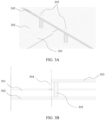
- FIG. 3A is a diagram of a structure of a transmission line connection structure according to an embodiment of this application. As shown in FIG. 3A , in a first part, a conductor strip 301 and a first ground layer 302 form a first transmission line (a microstrip structure).
- FIG. 3B is a side view of the transmission line connection structure shown in FIG. 3A .
- 304 is the transfer location between the first transmission line and the second transmission line.
- ground rods 305 are added near the transfer location 304 between the two transmission lines to perform transition, so that impact caused by field transfer discontinuity is reduced and a network loss is reduced.
- the ground rods 305 are generally ground screws, are located on two sides of the conductor strip 301 near the transfer location 304 between the microstrip and the stripline, and has a distance from the conductor strip 301.
- adding the ground screws may affect transmission line impedance matching, and sizes and locations of the ground screws are not flexibly adjusted, so that a standing wave ratio of the transmission line may be deteriorated.
- use of a form of screw ground rod may cause a passive intermodulation risk. Therefore, how to obtain a better transfer apparatus to transit transmission lines in different forms becomes an urgent problem to be resolved.
- embodiments of this application provide a transmission line connection structure.
- discontinuous ground layers are connected by using a coupling connection structure. This reduces a transmission loss, improves adjustment flexibility of the coupling connection structure, and can further avoid a passive intermodulation problem.
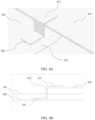
- FIG. 4A is a diagram of a structure of a transmission line connection structure according to an embodiment of this application.
- a coupling connection structure 401 is bridged between a first ground layer 302 and a second ground layer 303. Apart of a conductor strip 301 and the first ground layer 302 form a microstrip structure, to form a first transmission line. Behind a transfer location, the conductor strip 301 is located between the first ground layer 302 and the second ground layer 303, and forms a stripline structure with the first ground layer 302 and the second ground layer 303, to form a second transmission line.
- a part of the coupling connection structure 401 is coupled to the first ground layer 302, and another part is coupled to the second ground layer 303.
- the coupling connection structure 401 is located on one side of the conductor strip 301.
- An insulation medium 402 exists between the coupling connection structure 401 and each of the first ground layer 302 and the second ground layer 303.
- FIG. 4B is a side view of the transmission line connection structure shown in FIG. 4A .
- the coupling connection structure 401 is divided into three parts, including a first coupling section 101, a second coupling section 102, and a third coupling section 103.
- a conductor part of the first coupling section 101 is coupled to the first ground layer 302
- a conductor part of the third coupling section 103 is coupled to the second ground layer 303
- the second coupling section 102 is connected to the first coupling section 101 and the third coupling section 103.
- a plane on which the first coupling section 101 is located is parallel to a plane on which the third coupling section 103 is located, and a plane on which the second coupling section 102 is located is perpendicular to both the plane on which the first coupling section 101 is located and the plane on which the third coupling section 103 is located. It may be understood that, the plane on which the first coupling section 101 is located may not be absolutely parallel to the plane on which the third coupling section 103 is located, and a proper tilt angle also falls within the protection scope of this embodiment of this application. This is not specifically limited.
- the coupling connection structure 401 is used as a transition structure near the transfer location between a microstrip and a stripline, so that a loss caused by field discontinuity can be greatly reduced, a parasitic resonance mode in an operating frequency band can be fully suppressed, and a transmission loss can be reduced.
- a location of the coupling connection structure 401 may be more flexibly adjusted, so that transmission line impedance matching is properly controlled.
- a passive intermodulation risk can be avoided by using the coupling connection structure. Therefore, the transmission line connection structure has better performance, and transmission efficiency can be further improved when signal transmission is performed between different transmission lines.
- the coupling connection structure 401 because the second coupling section 102 is perpendicular to the first coupling section 101 and the third coupling section 103, a volume of the coupling connection structure 401 is small. This is more conducive to arrangement of the coupling connection structure 401 at a transfer location between different transmission lines.
- the coupling connection structure 401 may be distributed on one side of the conductor strip 301, or may be distributed on each of two sides of the conductor strip 301.
- distribution locations of the coupling connection structures 401 on the two sides of the conductor strip 301 are symmetrical. This further reduces impact caused by the field discontinuity, and improves the signal transmission efficiency.
- a plurality of coupling connection structures 401 on the two sides may share a part of the coupling sections.
- FIG. 5A is a diagram of a structure of another transmission line connection structure according to an embodiment of this application.
- a conductor strip 301 has a coupling connection structure on each of two sides, and two coupling connection structures may share a third coupling section 103, so that the coupling connection structure bypasses the conductor strip 301 and is bridged between a first ground layer 302 and a second ground layer 303.
- a part of the conductor strip 301 and the first ground layer 302 form a microstrip structure, to form a first transmission line. Behind a transfer location, the conductor strip 301 is located between the first ground layer 302 and the second ground layer 303, and forms a stripline structure with the first ground layer 302 and the second ground layer 303, to form a second transmission line.
- a part of the coupling connection structure is coupled to the first ground layer 302, and another part is coupled to the second ground layer 303.
- An insulation medium 402 exists between the coupling connection structure and each of the first ground layer 302 and the second ground layer 303.
- the coupling connection structure includes a first coupling connection structure and a second coupling connection structure.
- the first coupling connection structure includes a first coupling section 101, a second coupling section 102, and the third coupling section 103.
- the second coupling connection structure includes a fourth coupling section 104, a fifth coupling section 105, and the third coupling section 103.
- FIG. 5B is a side view of the transmission line connection structure shown in FIG. 5A .
- a conductor part of the first coupling section 101 and a conductor part of the fifth coupling section 105 are both coupled to the first ground layer 302, and a conductor part of the third coupling section 103 is coupled to the second ground layer 303.
- the second coupling section 102 is connected to the first coupling section 101 and the third coupling section 103, and the fourth coupling section 104 is connected to the fifth coupling section 105 and the third coupling section 103.
- the two coupling connection structures share the third coupling section 103 coupled to the second ground layer 303, so that a ⁇ -shaped structure is formed. This is more conducive to distribution of the coupling connection structure and improves integrity of the transmission line connection structure.
- FIG. 6A is a diagram of a structure of another transmission line connection structure according to an embodiment of this application.
- a second coupling section 102 is not perpendicular to a first coupling section 101 and a third coupling section 103, and the second coupling section 102 is tilted relative to a ground layer 601.
- a coupling connection structure is bridged between the ground layer 601 and a ground layer 602.
- a part of a conductor strip 603 and the ground layer 601 form a microstrip structure, to form a first transmission line.
- the other part of the conductor strip 603 is located between the ground layer 601 and the ground layer 602, and forms a suspended strip structure with the ground layer 601 and the ground layer 602, to form a second transmission line.
- a part of the coupling connection structure is coupled to the ground layer 601, and another part is coupled to the ground layer 602.
- An insulation medium 402 exists between the coupling connection structure and each of the ground layer 601 and the ground layer 602.
- FIG. 6B is a side view of the transmission line connection structure shown in FIG. 6A .
- the coupling connection structure is divided into three parts, including the first coupling section 101, the second coupling section 102, and the third coupling section 103.
- a conductor part of the first coupling section 101 is coupled to the ground layer 601
- a conductor part of the third coupling section 103 is coupled to the ground layer 602
- the second coupling section 102 is connected to the first coupling section 101 and the third coupling section 103.
- a plane on which the first coupling section 101 is located is parallel to a plane on which the third coupling section 103 is located, and an angle is formed between the second coupling section 102 and the ground layer 601.
- the angle between the second coupling section 102 and the ground layer 601 is a tilt angle of the coupling transition structure, namely, an angle between a projection of the second coupling section 102 on the ground layer 601 and the second coupling section 102.
- the coupling connection structure is formed by combining two coupling connection structures 401 located on two sides of the conductor strip 603.
- the conductor strip 603 may alternatively have one coupling connection structure on only one side, and a second coupling section 102 in the coupling connection structure is also tilted. This is not specifically limited.
- a loss caused by field discontinuity may be reduced, but impedance matching of the conductor strip 603 may be affected.
- a location of the coupling connection structure may be adjusted, and the tilt angle of the coupling transition structure may be adjusted. For example, the tilt angle of the coupling transition structure decreases, so that a field change becomes smoother. This can further reduce the loss.
- impact on the impedance matching is also reduced, and a voltage standing wave ratio decreases constantly.
- a structure of the second coupling section 102 in the coupling connection structure is changed, so that adjustment flexibility of the coupling connection structure can be improved.
- the tilt angle of the coupling connection structure is adjusted, so that the impedance matching can be improved, and the standing wave ratio decreases.
- the second coupling section 102 is tilted, so that the field change becomes smoother. This further reduces the loss, and improves signal transmission performance of the transmission line connection structure.
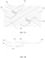
- FIG. 7A is a diagram of a structure of another transmission line connection structure according to an embodiment of this application.
- a coupling connection structure is used at a transfer location between a microstrip (a first transmission line) and a coplanar waveguide strip (a second transmission line).
- the coupling connection structure 401 is bridged between a ground layer 701 and a ground layer 702.
- a conductor strip 703 and the ground layer 702 are located on a same horizontal plane.
- a part of the conductor strip 703 and the ground layer 701 form a microstrip structure, to form the first transmission line.
- the other part of the conductor strip 703 is located between ground layers 702.
- the conductor strip 703 has a ground layer 702 on a left side and a ground layer 702 on a right side.
- the conductor strip 703 and the ground layer 702 form a coplanar waveguide strip structure, to form the second transmission line.
- a part of the coupling connection structure 401 is coupled to the ground layer 701, and another part is coupled to the ground layer 702.
- the coupling connection structure 401 may be located only on one side of the conductor strip 703, or may exist on each of two sides.
- An insulation medium 402 exists between the coupling connection structure 401 and each of the ground layer 701 and the ground layer
- FIG. 7B is a side view of the transmission line connection structure shown in FIG. 7A .
- the coupling connection structure 401 is divided into three parts, including a first coupling section 101, a second coupling section 102, and a third coupling section 103.
- a conductor part of the first coupling section 101 is coupled to the ground layer 701
- a conductor part of the third coupling section 103 is coupled to the ground layer 702
- the second coupling section 102 is connected to the first coupling section 101 and the third coupling section 103.
- a plane on which the first coupling section 101 is located is parallel to a plane on which the third coupling section 103 is located, and a plane on which the second coupling section 102 is located may be perpendicular or tilted to the plane on which the first coupling section 101 is located on and the plane on which the third coupling section 103 is located, so that an angle is formed between a projection of the second coupling section 102 on the ground layer 701 and the second coupling section 102.
- the plane on which the first coupling section 101 is located may not be absolutely parallel to the plane on which the third coupling section 103 is located, and a proper tilt angle also falls within the protection scope of this embodiment of this application. This is not specifically limited.
- a transition structure that is coupled to the ground layer 701 and the ground layer 702 is used on one side or each of two sides of the conductor strip 703, so that impact of field transfer discontinuity and impact of ground layer discontinuity are reduced, and a loss is greatly reduced.
- a location of the coupling connection structure 401 may be more flexibly adjusted, so that transmission line impedance matching is properly controlled.
- a passive intermodulation risk can be avoided by using the coupling connection structure. Therefore, the transmission line connection structure has better performance, and transmission efficiency is further improved when signal transmission is performed between different transmission lines.
- FIG. 8A is a diagram of a structure of another transmission line connection structure according to an embodiment of this application.
- a coupling connection structure is used at a transfer location between a microstrip (a first transmission line) and a ground coplanar waveguide strip (a second transmission line).
- the coupling connection structure 401 is bridged between a ground layer 801 and a ground layer 802.
- a conductor strip 803 and the ground layer 802 are located on a same horizontal plane.
- a part of the conductor strip 803 and the ground layer 801 form a microstrip structure, to form the first transmission line.
- the other part of the conductor strip 803 is located between ground layers 802.
- the conductor strip 803 has a ground layer 802 on a left side and a ground layer 802 on a right side.
- the conductor strip 803, the ground layer 801, and the ground layer 802 jointly form a ground coplanar waveguide strip structure, to form the second transmission line.
- a part of the coupling connection structure 401 is coupled to the ground layer 801, and another part is coupled to the ground layer 802.
- the coupling connection structure 401 may be located only on one side of the conductor strip 803, or may exist on each of two sides.
- An insulation medium 402 exists between the coupling connection structure 401 and each of the ground layer 801 and the ground layer 802.
- FIG. 8B is a side view of the transmission line connection structure shown in FIG. 8A .
- the coupling connection structure 401 is divided into three parts, including a first coupling section 101, a second coupling section 102, and a third coupling section 103.
- a conductor part of the first coupling section 101 is coupled to the ground layer 801
- a conductor part of the third coupling section 103 is coupled to the ground layer 802
- the second coupling section 102 is connected to the first coupling section 101 and the third coupling section 103.
- a plane on which the first coupling section 101 is located is parallel to a plane on which the third coupling section 103 is located, and a plane on which the second coupling section 102 is located may be perpendicular or tilted to the plane on which the first coupling section 101 is located and the plane on which the third coupling section 103 is located, so that an acute angle is formed between a projection of the second coupling section 102 on the ground layer 801 and the second coupling section 102.
- a transition structure that is coupled to the ground layer 801 and the ground layer 802 is used on one side or each of two sides of the conductor strip 803, so that impact of field transfer discontinuity and impact of ground layer discontinuity are reduced, and a loss is greatly reduced.
- a location of the coupling connection structure 401 may be more flexibly adjusted, so that transmission line impedance matching is properly controlled.
- a passive intermodulation risk can be avoided by using the coupling connection structure. Therefore, the transmission line connection structure has better performance, and transmission efficiency is further improved when signal transmission is performed between different transmission lines.
- FIG. 9A is a diagram of a structure of another transmission line connection structure according to an embodiment of this application.
- a multi-coupling connection structure is used at a plurality of transfer locations between a microstrip (a first transmission line) and a suspended strip (a second transmission line).
- the multi-coupling connection structure is bridged between a ground layer 901 and a ground layer 902.
- a conductor strip enters and exits from the ground layer 902 for a plurality of times.
- a part of the conductor strip 903 and the ground layer 901 form a microstrip structure, to form the first transmission line.
- the other part is located between the ground layer 901 and the ground layer 902, and the conductor strip 903, the ground layer 901, and the ground layer 902 jointly form a suspended strip structure, to form the second transmission line.
- Apart of the multi-coupling connection structure is coupled to the ground layer 901, and another part is coupled to the ground layer 902.
- the multi-coupling connection structure is bridged between a plurality of sections of the conductor strip 903.
- An insulation medium 402 exists between the multi-coupling connection structure and each of the ground layer 901 and the ground layer 902.
- FIG. 9B is a side view of the transmission line connection structure shown in FIG. 9A .
- the multi-coupling connection structure is divided into a plurality of coupling sections, and there is a coupling connection structure on each of two sides of each section of the conductor strip 903. Coupling connection structures in two adjacent sections of the conductor strip 903 are used as an example.
- a multi-coupling connection structure may include four coupling connection structures.
- a first coupling connection structure is located on a first side of a first section of the conductor strip 903.
- a second coupling connection structure is located on a second side of the first section of the conductor strip 903.
- a third coupling connection structure is located on a first side of a second section of the conductor strip 903.
- a fourth coupling connection structure is located on a second side of the second section of the conductor strip 903.
- the first coupling connection structure and the second coupling connection structure share one coupling section coupled to the ground layer 902.
- the second coupling connection structure and the third coupling connection structure share one coupling section coupled to the ground layer 901.
- the third coupling connection structure and the fourth coupling connection structure share one coupling section coupled to the ground layer 901.
- a conductor part of a first coupling section is coupled to the ground layer 901, a conductor part of a third coupling section is coupled to the ground layer 902, and a second coupling section is connected to the first coupling section and the third coupling section.
- a plane on which the first coupling section is located is parallel to a plane on which the third coupling section is located, and a plane on which the second coupling section is located may be perpendicular or tilted to the plane on which the first coupling section is located and the plane on which the second coupling section is located, so that an acute angle is formed between a projection of the second coupling section on the ground layer 901 and the second coupling section.
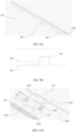
- connection structure includes two conductor strips: a conductor strip 1001 and a conductor strip 1002.
- a part of the conductor strip 1001 and a ground layer 1003 form a microstrip structure (a first transmission line), and the other part forms a suspended strip structure (a second transmission line) together with the ground layer 1003 and a ground layer 1004.
- a part of the conductor strip 1002 and the ground layer 1003 form a microstrip structure (a third transmission line), and the other part forms a suspended strip structure (a fourth transmission line) together with the ground layer 1003 and a ground layer 1005.
- a coupling connection structure 1006 is bridged between the ground layer 1003, the ground layer 1004, and the ground layer 1005.
- the coupling connection structure 1006 includes a first coupling section 101, a second coupling section 102, a third coupling section 103, a fourth coupling section 104, and a fifth coupling section 105.
- a conductor part of the first coupling section 101 is coupled to the ground layer 1003, a conductor part of the third coupling section 103 is coupled to the ground layer 1004, and the second coupling section 102 is connected to the first coupling section 101 and the third coupling section 103.
- a conductor part of the fifth coupling section 105 is coupled to the ground layer 1005, and the fourth coupling section 104 is connected to the first coupling section 101 and the fifth coupling section 105.
- FIG. 10B is a side view of the transmission line connection structure shown in FIG. 10A .
- a transition structure that is coupled to the ground layer 1003, the ground layer 1004, and the ground layer 1005 is used near a transfer location that is of a double-line structure and that is between a microstrip and a suspended strip, to reduce a transfer loss and improve isolation between the two lines.
- a specific implementation of the solution is that a first feed conductor strip 1010, a first short-circuit conductor strip 1011, and a first feed coaxial cable 1013 form a first feed structure, and are coupled to the conductor strip 1001 by using an insulation medium.
- a second feed conductor strip 1020, a second short-circuit conductor strip 1021, and a second feed coaxial cable 1023 form a second feed structure, and are coupled to the conductor strip 1002 by using an insulation medium.
- the coupling connection structure is used, to reduce impact of field transfer discontinuity and ground layer discontinuity, and greatly reduce a loss.
- a location of the coupling connection structure may be more flexibly adjusted, so that transmission line impedance matching is properly controlled.
- a passive intermodulation risk can be avoided by using the coupling connection structure and the isolation between the two lines can be improved. Therefore, the transmission line connection structure has better performance, and transmission efficiency is further improved when signal transmission is performed between different transmission lines.
Landscapes
- Engineering & Computer Science (AREA)
- Computer Networks & Wireless Communication (AREA)
- Waveguide Connection Structure (AREA)
- Waveguides (AREA)
Applications Claiming Priority (2)
| Application Number | Priority Date | Filing Date | Title |
|---|---|---|---|
| CN202111538192.8A CN116264356A (zh) | 2021-12-15 | 2021-12-15 | 一种传输线连接结构 |
| PCT/CN2022/137425 WO2023109628A1 (zh) | 2021-12-15 | 2022-12-08 | 一种传输线连接结构 |
Publications (2)
| Publication Number | Publication Date |
|---|---|
| EP4421994A1 true EP4421994A1 (de) | 2024-08-28 |
| EP4421994A4 EP4421994A4 (de) | 2025-02-26 |
Family
ID=86723524
Family Applications (1)
| Application Number | Title | Priority Date | Filing Date |
|---|---|---|---|
| EP22906376.3A Pending EP4421994A4 (de) | 2021-12-15 | 2022-12-08 | Übertragungsleitungsverbindungsstruktur |
Country Status (4)
| Country | Link |
|---|---|
| US (1) | US12658548B2 (de) |
| EP (1) | EP4421994A4 (de) |
| CN (1) | CN116264356A (de) |
| WO (1) | WO2023109628A1 (de) |
Family Cites Families (14)
| Publication number | Priority date | Publication date | Assignee | Title |
|---|---|---|---|---|
| US4862120A (en) * | 1988-02-29 | 1989-08-29 | Canadian Patents And Development Limited/Societe Canadienne Des Brevets Et D'exploitation Limitee | Wideband stripline to microstrip transition |
| FR2772518B1 (fr) * | 1997-12-11 | 2000-01-07 | Alsthom Cge Alcatel | Antenne a court-circuit realisee selon la technique des microrubans et dispositif incluant cette antenne |
| GB2337859B (en) * | 1998-05-29 | 2002-12-11 | Nokia Mobile Phones Ltd | Antenna |
| US6621466B2 (en) * | 2001-06-19 | 2003-09-16 | Tyco Electronics Logistics Ag | Multiple band split ground plane antenna assembly |
| US6933450B2 (en) * | 2002-06-27 | 2005-08-23 | Kyocera Corporation | High-frequency signal transmitting device |
| US7315223B2 (en) * | 2004-06-30 | 2008-01-01 | Emag Technologies, Inc. | Microstrip-to-microstrip RF transition including co-planar waveguide connected by vias |
| US7710338B2 (en) * | 2007-05-08 | 2010-05-04 | Panasonic Corporation | Slot antenna apparatus eliminating unstable radiation due to grounding structure |
| JP4737192B2 (ja) * | 2007-12-21 | 2011-07-27 | トヨタ自動車株式会社 | 2つのマイクロストリップ線路の接続構造及び筐体を用いた集積回路チップの実装基板への実装構造 |
| CN102738550B (zh) * | 2011-04-06 | 2014-11-05 | 安德鲁公司 | 带状线至微带线的电容耦合转换结构及包含该结构的天线 |
| US8912634B2 (en) * | 2012-03-29 | 2014-12-16 | International Business Machines Corporation | High frequency transition matching in an electronic package for millimeter wave semiconductor dies |
| CN103441325B (zh) * | 2013-08-15 | 2015-08-19 | 华为技术有限公司 | 一种通信天线系统 |
| EP3249741B1 (de) * | 2016-05-24 | 2020-02-26 | Nokia Shanghai Bell Co., Ltd. | Vorrichtung zur verbindung zwischen einer streifenleitung und einem koaxialkabel |
| KR102057314B1 (ko) * | 2018-11-26 | 2020-01-22 | 주식회사 센서뷰 | 밀리미터파(mmWave) 대역용 전송선로 일체형 저손실 유연 다중 포트 안테나 |
| CN113594658B (zh) * | 2021-08-11 | 2022-04-08 | 上海交通大学 | 接地共面波导到悬置微带线的宽带过渡结构 |
-
2021
- 2021-12-15 CN CN202111538192.8A patent/CN116264356A/zh active Pending
-
2022
- 2022-12-08 WO PCT/CN2022/137425 patent/WO2023109628A1/zh not_active Ceased
- 2022-12-08 EP EP22906376.3A patent/EP4421994A4/de active Pending
-
2024
- 2024-05-23 US US18/672,016 patent/US12658548B2/en active Active
Also Published As
| Publication number | Publication date |
|---|---|
| US12658548B2 (en) | 2026-06-16 |
| EP4421994A4 (de) | 2025-02-26 |
| US20240313382A1 (en) | 2024-09-19 |
| CN116264356A (zh) | 2023-06-16 |
| WO2023109628A1 (zh) | 2023-06-22 |
Similar Documents
| Publication | Publication Date | Title |
|---|---|---|
| CN114883797B (zh) | 双频双极化天线单元、子阵移相模块及相控阵天线阵列 | |
| CN112117533A (zh) | 双频双线极化相控阵天线及天线单元 | |
| WO2020233477A1 (zh) | 天线单元及终端设备 | |
| EP4407803A1 (de) | Antenne und basisstationsvorrichtung | |
| CN114765300B (zh) | 天线装置及电子设备 | |
| CN112751180B (zh) | 天线模组及电子设备 | |
| US20230335902A1 (en) | Multi-band antenna and communication device | |
| CN114883773B (zh) | 一种天线结构、电子设备及无线网络系统 | |
| US20250329916A1 (en) | Base station antenna and base station system | |
| US12627021B2 (en) | Base station antenna | |
| EP4579956A1 (de) | Antennenvorrichtung und drahtloskommunikationsvorrichtung | |
| EP4564604A1 (de) | Antenne und kommunikationsvorrichtung | |
| CN110011049A (zh) | 一种加载寄生贴片的微带天线 | |
| US20260045688A1 (en) | Antenna apparatus, antenna system, and communication device | |
| CN111864407B (zh) | 一种准八木天线阵列及毫米波基站设备 | |
| US12113289B2 (en) | Dual-frequency and dual-polarization antenna array and electronic device | |
| US11923611B2 (en) | Dual-frequency and dual-polarization antenna and electronic device | |
| US20240313382A1 (en) | Transmission line connection structure | |
| US20220094077A1 (en) | Antenna structure and wireless communication device using same | |
| US20250087895A1 (en) | Antenna, communication device, and communication system | |
| CN116154472A (zh) | 双极化天线单元、天线模组及基站 | |
| CN116266673A (zh) | 一种天线和通信设备 | |
| US5877729A (en) | Wide-beam high gain base station communications antenna | |
| EP4629443A1 (de) | Speisevorrichtung, antennenvorrichtung und kommunikationsvorrichtung | |
| EP4513676A1 (de) | Antenne und basisstation |
Legal Events
| Date | Code | Title | Description |
|---|---|---|---|
| STAA | Information on the status of an ep patent application or granted ep patent |
Free format text: STATUS: THE INTERNATIONAL PUBLICATION HAS BEEN MADE |
|
| PUAI | Public reference made under article 153(3) epc to a published international application that has entered the european phase |
Free format text: ORIGINAL CODE: 0009012 |
|
| STAA | Information on the status of an ep patent application or granted ep patent |
Free format text: STATUS: REQUEST FOR EXAMINATION WAS MADE |
|
| 17P | Request for examination filed |
Effective date: 20240523 |
|
| AK | Designated contracting states |
Kind code of ref document: A1 Designated state(s): AL AT BE BG CH CY CZ DE DK EE ES FI FR GB GR HR HU IE IS IT LI LT LU LV MC ME MK MT NL NO PL PT RO RS SE SI SK SM TR |
|
| REG | Reference to a national code |
Ref country code: DE Ref legal event code: R079 Free format text: PREVIOUS MAIN CLASS: H01Q0013080000 Ipc: H01P0005080000 |
|
| A4 | Supplementary search report drawn up and despatched |
Effective date: 20250127 |
|
| RIC1 | Information provided on ipc code assigned before grant |
Ipc: H01Q 1/24 20060101ALN20250121BHEP Ipc: H01P 5/08 20060101AFI20250121BHEP |
|
| DAV | Request for validation of the european patent (deleted) | ||
| DAX | Request for extension of the european patent (deleted) |