EP4424689A1 - Dérivés de 8,8-diméthyl-8h-thiéno[3',2':5,6]pyrido[3,2,1-jk]carbazole destinés à être utilisés dans des dispositifs photoélectriques - Google Patents
Dérivés de 8,8-diméthyl-8h-thiéno[3',2':5,6]pyrido[3,2,1-jk]carbazole destinés à être utilisés dans des dispositifs photoélectriques Download PDFInfo
- Publication number
- EP4424689A1 EP4424689A1 EP24159360.7A EP24159360A EP4424689A1 EP 4424689 A1 EP4424689 A1 EP 4424689A1 EP 24159360 A EP24159360 A EP 24159360A EP 4424689 A1 EP4424689 A1 EP 4424689A1
- Authority
- EP
- European Patent Office
- Prior art keywords
- group
- substituted
- unsubstituted
- chemical formula
- cyano
- Prior art date
- Legal status (The legal status is an assumption and is not a legal conclusion. Google has not performed a legal analysis and makes no representation as to the accuracy of the status listed.)
- Pending
Links
Images


Classifications
-
- C—CHEMISTRY; METALLURGY
- C07—ORGANIC CHEMISTRY
- C07D—HETEROCYCLIC COMPOUNDS
- C07D495/00—Heterocyclic compounds containing in the condensed system at least one hetero ring having sulfur atoms as the only ring hetero atoms
- C07D495/12—Heterocyclic compounds containing in the condensed system at least one hetero ring having sulfur atoms as the only ring hetero atoms in which the condensed system contains three hetero rings
- C07D495/14—Ortho-condensed systems
-
- C—CHEMISTRY; METALLURGY
- C07—ORGANIC CHEMISTRY
- C07D—HETEROCYCLIC COMPOUNDS
- C07D495/00—Heterocyclic compounds containing in the condensed system at least one hetero ring having sulfur atoms as the only ring hetero atoms
- C07D495/02—Heterocyclic compounds containing in the condensed system at least one hetero ring having sulfur atoms as the only ring hetero atoms in which the condensed system contains two hetero rings
- C07D495/04—Ortho-condensed systems
-
- H—ELECTRICITY
- H10—SEMICONDUCTOR DEVICES; ELECTRIC SOLID-STATE DEVICES NOT OTHERWISE PROVIDED FOR
- H10K—ORGANIC ELECTRIC SOLID-STATE DEVICES
- H10K30/00—Organic devices sensitive to infrared radiation, light, electromagnetic radiation of shorter wavelength or corpuscular radiation
- H10K30/60—Organic devices sensitive to infrared radiation, light, electromagnetic radiation of shorter wavelength or corpuscular radiation in which radiation controls flow of current through the devices, e.g. photoresistors
-
- C—CHEMISTRY; METALLURGY
- C07—ORGANIC CHEMISTRY
- C07D—HETEROCYCLIC COMPOUNDS
- C07D471/00—Heterocyclic compounds containing nitrogen atoms as the only ring hetero atoms in the condensed system, at least one ring being a six-membered ring with one nitrogen atom, not provided for by groups C07D451/00 - C07D463/00
- C07D471/02—Heterocyclic compounds containing nitrogen atoms as the only ring hetero atoms in the condensed system, at least one ring being a six-membered ring with one nitrogen atom, not provided for by groups C07D451/00 - C07D463/00 in which the condensed system contains two hetero rings
- C07D471/06—Peri-condensed systems
-
- C—CHEMISTRY; METALLURGY
- C07—ORGANIC CHEMISTRY
- C07D—HETEROCYCLIC COMPOUNDS
- C07D493/00—Heterocyclic compounds containing oxygen atoms as the only ring hetero atoms in the condensed system
- C07D493/02—Heterocyclic compounds containing oxygen atoms as the only ring hetero atoms in the condensed system in which the condensed system contains two hetero rings
- C07D493/06—Peri-condensed systems
-
- C—CHEMISTRY; METALLURGY
- C07—ORGANIC CHEMISTRY
- C07D—HETEROCYCLIC COMPOUNDS
- C07D495/00—Heterocyclic compounds containing in the condensed system at least one hetero ring having sulfur atoms as the only ring hetero atoms
- C07D495/12—Heterocyclic compounds containing in the condensed system at least one hetero ring having sulfur atoms as the only ring hetero atoms in which the condensed system contains three hetero rings
- C07D495/16—Peri-condensed systems
-
- C—CHEMISTRY; METALLURGY
- C07—ORGANIC CHEMISTRY
- C07D—HETEROCYCLIC COMPOUNDS
- C07D495/00—Heterocyclic compounds containing in the condensed system at least one hetero ring having sulfur atoms as the only ring hetero atoms
- C07D495/22—Heterocyclic compounds containing in the condensed system at least one hetero ring having sulfur atoms as the only ring hetero atoms in which the condensed system contains four or more hetero rings
-
- C—CHEMISTRY; METALLURGY
- C07—ORGANIC CHEMISTRY
- C07D—HETEROCYCLIC COMPOUNDS
- C07D513/00—Heterocyclic compounds containing in the condensed system at least one hetero ring having nitrogen and sulfur atoms as the only ring hetero atoms, not provided for in groups C07D463/00, C07D477/00 or C07D499/00 - C07D507/00
- C07D513/12—Heterocyclic compounds containing in the condensed system at least one hetero ring having nitrogen and sulfur atoms as the only ring hetero atoms, not provided for in groups C07D463/00, C07D477/00 or C07D499/00 - C07D507/00 in which the condensed system contains three hetero rings
- C07D513/14—Ortho-condensed systems
-
- C—CHEMISTRY; METALLURGY
- C07—ORGANIC CHEMISTRY
- C07D—HETEROCYCLIC COMPOUNDS
- C07D513/00—Heterocyclic compounds containing in the condensed system at least one hetero ring having nitrogen and sulfur atoms as the only ring hetero atoms, not provided for in groups C07D463/00, C07D477/00 or C07D499/00 - C07D507/00
- C07D513/12—Heterocyclic compounds containing in the condensed system at least one hetero ring having nitrogen and sulfur atoms as the only ring hetero atoms, not provided for in groups C07D463/00, C07D477/00 or C07D499/00 - C07D507/00 in which the condensed system contains three hetero rings
- C07D513/16—Peri-condensed systems
-
- C—CHEMISTRY; METALLURGY
- C07—ORGANIC CHEMISTRY
- C07F—ACYCLIC, CARBOCYCLIC OR HETEROCYCLIC COMPOUNDS CONTAINING ELEMENTS OTHER THAN CARBON, HYDROGEN, HALOGEN, OXYGEN, NITROGEN, SULFUR, SELENIUM OR TELLURIUM
- C07F7/00—Compounds containing elements of Groups 4 or 14 of the Periodic Table
- C07F7/02—Silicon compounds
- C07F7/08—Compounds having one or more C—Si linkages
- C07F7/0803—Compounds with Si-C or Si-Si linkages
- C07F7/081—Compounds with Si-C or Si-Si linkages comprising at least one atom selected from the elements N, O, halogen, S, Se or Te
- C07F7/0812—Compounds with Si-C or Si-Si linkages comprising at least one atom selected from the elements N, O, halogen, S, Se or Te comprising a heterocyclic ring
- C07F7/0816—Compounds with Si-C or Si-Si linkages comprising at least one atom selected from the elements N, O, halogen, S, Se or Te comprising a heterocyclic ring said ring comprising Si as a ring atom
-
- G—PHYSICS
- G01—MEASURING; TESTING
- G01N—INVESTIGATING OR ANALYSING MATERIALS BY DETERMINING THEIR CHEMICAL OR PHYSICAL PROPERTIES
- G01N21/00—Investigating or analysing materials by the use of optical means, i.e. using sub-millimetre waves, infrared, visible or ultraviolet light
- G01N21/17—Systems in which incident light is modified in accordance with the properties of the material investigated
- G01N21/25—Colour; Spectral properties, i.e. comparison of effect of material on the light at two or more different wavelengths or wavelength bands
- G01N21/27—Colour; Spectral properties, i.e. comparison of effect of material on the light at two or more different wavelengths or wavelength bands using photo-electric detection ; circuits for computing concentration
-
- G—PHYSICS
- G06—COMPUTING OR CALCULATING; COUNTING
- G06V—IMAGE OR VIDEO RECOGNITION OR UNDERSTANDING
- G06V10/00—Arrangements for image or video recognition or understanding
- G06V10/10—Image acquisition
- G06V10/12—Details of acquisition arrangements; Constructional details thereof
- G06V10/14—Optical characteristics of the device performing the acquisition or on the illumination arrangements
- G06V10/143—Sensing or illuminating at different wavelengths
-
- G—PHYSICS
- G06—COMPUTING OR CALCULATING; COUNTING
- G06V—IMAGE OR VIDEO RECOGNITION OR UNDERSTANDING
- G06V10/00—Arrangements for image or video recognition or understanding
- G06V10/10—Image acquisition
- G06V10/12—Details of acquisition arrangements; Constructional details thereof
- G06V10/14—Optical characteristics of the device performing the acquisition or on the illumination arrangements
- G06V10/147—Details of sensors, e.g. sensor lenses
-
- H—ELECTRICITY
- H10—SEMICONDUCTOR DEVICES; ELECTRIC SOLID-STATE DEVICES NOT OTHERWISE PROVIDED FOR
- H10K—ORGANIC ELECTRIC SOLID-STATE DEVICES
- H10K30/00—Organic devices sensitive to infrared radiation, light, electromagnetic radiation of shorter wavelength or corpuscular radiation
- H10K30/80—Constructional details
- H10K30/81—Electrodes
-
- H—ELECTRICITY
- H10—SEMICONDUCTOR DEVICES; ELECTRIC SOLID-STATE DEVICES NOT OTHERWISE PROVIDED FOR
- H10K—ORGANIC ELECTRIC SOLID-STATE DEVICES
- H10K39/00—Integrated devices, or assemblies of multiple devices, comprising at least one organic radiation-sensitive element covered by group H10K30/00
- H10K39/30—Devices controlled by radiation
- H10K39/32—Organic image sensors
- H10K39/34—Organic image sensors integrated with organic light-emitting diodes [OLED]
-
- H—ELECTRICITY
- H10—SEMICONDUCTOR DEVICES; ELECTRIC SOLID-STATE DEVICES NOT OTHERWISE PROVIDED FOR
- H10K—ORGANIC ELECTRIC SOLID-STATE DEVICES
- H10K59/00—Integrated devices, or assemblies of multiple devices, comprising at least one organic light-emitting element covered by group H10K50/00
- H10K59/30—Devices specially adapted for multicolour light emission
- H10K59/35—Devices specially adapted for multicolour light emission comprising red-green-blue [RGB] subpixels
-
- H—ELECTRICITY
- H10—SEMICONDUCTOR DEVICES; ELECTRIC SOLID-STATE DEVICES NOT OTHERWISE PROVIDED FOR
- H10K—ORGANIC ELECTRIC SOLID-STATE DEVICES
- H10K65/00—Integrated devices, or assemblies of multiple devices, comprising at least one organic light-emitting element and at least one organic radiation-sensitive element, e.g. organic opto-couplers
-
- H—ELECTRICITY
- H10—SEMICONDUCTOR DEVICES; ELECTRIC SOLID-STATE DEVICES NOT OTHERWISE PROVIDED FOR
- H10K—ORGANIC ELECTRIC SOLID-STATE DEVICES
- H10K85/00—Organic materials used in the body or electrodes of devices covered by this subclass
- H10K85/40—Organosilicon compounds, e.g. TIPS pentacene
-
- H—ELECTRICITY
- H10—SEMICONDUCTOR DEVICES; ELECTRIC SOLID-STATE DEVICES NOT OTHERWISE PROVIDED FOR
- H10K—ORGANIC ELECTRIC SOLID-STATE DEVICES
- H10K85/00—Organic materials used in the body or electrodes of devices covered by this subclass
- H10K85/60—Organic compounds having low molecular weight
- H10K85/615—Polycyclic condensed aromatic hydrocarbons, e.g. anthracene
- H10K85/621—Aromatic anhydride or imide compounds, e.g. perylene tetra-carboxylic dianhydride or perylene tetracarboxylic di-imide
-
- H—ELECTRICITY
- H10—SEMICONDUCTOR DEVICES; ELECTRIC SOLID-STATE DEVICES NOT OTHERWISE PROVIDED FOR
- H10K—ORGANIC ELECTRIC SOLID-STATE DEVICES
- H10K85/00—Organic materials used in the body or electrodes of devices covered by this subclass
- H10K85/60—Organic compounds having low molecular weight
- H10K85/649—Aromatic compounds comprising a hetero atom
- H10K85/654—Aromatic compounds comprising a hetero atom comprising only nitrogen as heteroatom
-
- H—ELECTRICITY
- H10—SEMICONDUCTOR DEVICES; ELECTRIC SOLID-STATE DEVICES NOT OTHERWISE PROVIDED FOR
- H10K—ORGANIC ELECTRIC SOLID-STATE DEVICES
- H10K85/00—Organic materials used in the body or electrodes of devices covered by this subclass
- H10K85/60—Organic compounds having low molecular weight
- H10K85/649—Aromatic compounds comprising a hetero atom
- H10K85/657—Polycyclic condensed heteroaromatic hydrocarbons
- H10K85/6574—Polycyclic condensed heteroaromatic hydrocarbons comprising only oxygen in the heteroaromatic polycondensed ring system, e.g. cumarine dyes
-
- H—ELECTRICITY
- H10—SEMICONDUCTOR DEVICES; ELECTRIC SOLID-STATE DEVICES NOT OTHERWISE PROVIDED FOR
- H10K—ORGANIC ELECTRIC SOLID-STATE DEVICES
- H10K85/00—Organic materials used in the body or electrodes of devices covered by this subclass
- H10K85/60—Organic compounds having low molecular weight
- H10K85/649—Aromatic compounds comprising a hetero atom
- H10K85/657—Polycyclic condensed heteroaromatic hydrocarbons
- H10K85/6576—Polycyclic condensed heteroaromatic hydrocarbons comprising only sulfur in the heteroaromatic polycondensed ring system, e.g. benzothiophene
-
- H—ELECTRICITY
- H10—SEMICONDUCTOR DEVICES; ELECTRIC SOLID-STATE DEVICES NOT OTHERWISE PROVIDED FOR
- H10K—ORGANIC ELECTRIC SOLID-STATE DEVICES
- H10K30/00—Organic devices sensitive to infrared radiation, light, electromagnetic radiation of shorter wavelength or corpuscular radiation
- H10K30/30—Organic devices sensitive to infrared radiation, light, electromagnetic radiation of shorter wavelength or corpuscular radiation comprising bulk heterojunctions, e.g. interpenetrating networks of donor and acceptor material domains
-
- Y—GENERAL TAGGING OF NEW TECHNOLOGICAL DEVELOPMENTS; GENERAL TAGGING OF CROSS-SECTIONAL TECHNOLOGIES SPANNING OVER SEVERAL SECTIONS OF THE IPC; TECHNICAL SUBJECTS COVERED BY FORMER USPC CROSS-REFERENCE ART COLLECTIONS [XRACs] AND DIGESTS
- Y02—TECHNOLOGIES OR APPLICATIONS FOR MITIGATION OR ADAPTATION AGAINST CLIMATE CHANGE
- Y02E—REDUCTION OF GREENHOUSE GAS [GHG] EMISSIONS, RELATED TO ENERGY GENERATION, TRANSMISSION OR DISTRIBUTION
- Y02E10/00—Energy generation through renewable energy sources
- Y02E10/50—Photovoltaic [PV] energy
- Y02E10/549—Organic PV cells
Definitions
- Example embodiments relate to compounds, photoelectric devices, light absorption sensors, sensor-embedded display panels, and electronic devices.
- a display device implementing a biometric recognition technology that authenticates the person by extracting specific biometric information or behavioral characteristic information of a person with an automated device, centering on finance, healthcare, and mobile device. Accordingly, research is being conducted on a display device including a sensor capable of biometric recognition.
- Such a sensor capable of biometric recognition may be disposed under a display panel of a display device or may be separately manufactured as a separate module and mounted outside the display device.
- the sensor is configured to recognize an object recognized through the display panel, various films, and/or parts with improved performance and having improved integration overcoming limitations in terms of design and usability that may be associated with sensors manufactured and mounted as separate modules. Accordingly, a sensor-embedded display panel including a sensor capable of improving performance by being integrated with the display panel has been proposed.
- the photoelectric device used in the sensor as described above is a device that converts light into an electrical signal using the photoelectric effect, and may include a photodiode and a phototransistor.
- a sensor e.g., an image sensor
- a photodiode has a higher resolution and a smaller pixel size.
- a silicon photodiode is widely used, but it has a problem of deteriorated sensitivity since silicon photodiode has a smaller absorption area due to small pixels. Accordingly, an organic material that is capable of replacing silicon has been researched.
- the organic material has a high extinction coefficient and selectively absorbs light in a particular wavelength region depending on a molecular structure, and thus may simultaneously replace a photodiode and a color filter and resultantly improve sensitivity and contribute to high integration.
- Some example embodiments provide a compound that can selectively absorb light in a visible light region and improve light absorption characteristics of a device.
- Some example embodiments provide a photoelectric device that selectively absorbs light in the visible light region and has improved light absorption characteristics of the device.
- Some example embodiments provide a (light absorption) sensor including the photoelectric device.
- Some example embodiments provide a sensor-embedded display panel including the photoelectric device or (light absorption) sensor.
- Some example embodiments provide an electronic device including the photoelectric device or (light absorption) sensor.
- a compound may be represented by Chemical Formula 1, and the compound may have a reorganization energy of the compound of less than about 0.163 eV and a maximum absorption wavelength value calculated by density functional theory (DFT) of less than or equal to about 495 nm.
- DFT density functional theory
- Chemical Formula 1 may include a carbazolyl ring group that includes a benzene ring.
- nitrogen (N) may be included at position 1 of the carbazolyl ring group.
- R x , R y , and R z may each independently be hydrogen or an electron donating group selected from a C1 to C10 alkyl group and a C1 to C10 alkoxy group.
- Chemical Formula 1 may include a ring structure.
- the ring structure may be a substituted or unsubstituted C5 to C30 hydrocarbon ring group or a substituted or unsubstituted C2 to C30 heterocyclic group.
- the ring structure may include a moiety represented by Chemical Formula 2.
- the ring structure may include one of the moieties represented by Chemical Formula 3.
- At least one CH present in the aromatic ring of moiety (3), (4), (5), (6), (7), (8), or (9) may be replaced by N.
- EWG may be a cyclic group represented by Chemical Formula 4.
- EWG may be a cyclic group represented by any one of Chemical Formula 5A to Chemical Formula 5H.
- the compound may have a polarizability of less than or equal to about 500 bhor 3 .
- the compound may have an oscillator strength value of greater than or equal to about 0.8.
- the dipole moment of the compound may be greater than or equal to about 3 Debye (D).
- the compound may have a maximum absorption wavelength ( ⁇ max ) in a wavelength range of about 500 nm to about 540 nm in a thin film state.
- a sublimation temperature of the compound represented by Chemical Formula 1 may be less than or equal to about 280 °C.
- the compound may exhibit an absorption curve with a full width at half maximum (FWHM) of less than or equal to about 150 nm in a thin film state.
- FWHM full width at half maximum
- a photoelectric device e.g., organic photoelectric device
- a photoelectric device includes a first electrode and a second electrode facing each other, and
- the light absorbing layer may be configured to absorb light of a red wavelength spectrum, a green wavelength spectrum, a blue wavelength spectrum, an infrared wavelength spectrum, or any combination thereof.
- a light absorption sensor including the photoelectric device is provided.
- the light absorption sensor may include a semiconductor substrate integrated with a plurality of first photo-sensing devices configured to sense light in a blue wavelength region and a plurality of second photo-sensing devices configured to sense light in a red wavelength region, and the photoelectric device may be a green photoelectric device configured to sense light in a green wavelength region and may be on the semiconductor substrate.
- the light absorbing layer may include a p-type semiconductor and an n-type semiconductor, the p-type semiconductor includes the compound represented by Chemical Formula 1, and the n-type semiconductor includes fullerene, a fullerene derivative, sub-phthalocyanine or a sub-phthalocyanine derivative, thiophene or a thiophene derivative, or a compound represented by Chemical Formula 6.
- the light absorption sensor may further include a color filter layer including a blue filter selectively transmitting light in a blue wavelength region and a red filter selectively transmitting light in a red wavelength region.
- the light absorption sensor may include the photoelectric device, wherein the photoelectric device is a green photoelectric device configured to sense light in a green wavelength region, the light absorption sensor further includes a semiconductor substrate integrated with a plurality of first photo-sensing devices configured to sense light in a blue wavelength region and a plurality of second photo-sensing devices configured to sense light in a red wavelength region, and the photoelectric device is on the semiconductor substrate.
- a sensor-embedded display panel may include a substrate, a light emitting element disposed on the substrate and including a light emitting layer, and a light absorption sensor disposed on the substrate and comprising a light absorbing layer, the light absorbing layer being arranged in parallel with the light emitting layer along an in-plane direction of the substrate such that the light absorbing layer and the light emitting layer at least partially overlap in the in-plane direction, wherein the light absorbing layer is configured to absorb light of a red wavelength spectrum, a green wavelength spectrum, a blue wavelength spectrum, an infrared wavelength spectrum, or any combination thereof, the light absorbing layer configured to absorb light of the green wavelength spectrum includes the compound represented by Chemical Formula 1.
- the light emitting element may include first, second and third light emitting elements configured to emit light of different wavelength spectra, and the light absorption sensor may be configured to absorb light emitted from at least one of the first, second, or third light emitting elements and then reflected by the recognition target to the light absorption sensor and to convert the absorbed light into an electrical signal.
- the light emitting element and the light absorption sensor may each include a separate portion of a common electrode configured to apply a common voltage to the light emitting element and the light absorption sensor, and the sensor-embedded display panel may further include a first common auxiliary layer that is a single piece of material that extends continuously between the light emitting layer and the common electrode and between the light absorbing layer and the common electrode.
- a difference between a LUMO energy level of the first common auxiliary layer and a LUMO energy level of the compound represented by Chemical Formula 1 may be less than or equal to about 1.2 eV.
- the sensor-embedded display panel may further include a second common auxiliary layer that is a single piece of material that extends continuously between the light emitting layer and the substrate and between the light absorbing layer and the substrate.
- the light emitting element may include first, second, and third light emitting elements configured to emit light of any one wavelength spectrum of the red wavelength spectrum, the green wavelength spectrum, or the blue wavelength spectrum, and the light absorbing layer may be configured to absorb light having a same wavelength spectrum as light emitted from at least one of the first, second, or third light emitting elements.
- the sensor-embedded display panel may include a display area configured to display a color and a non-display area excluding the display area, and the light absorption sensor may be in the non-display area.
- the display area may include a plurality of first subpixels configured to display light of the red wavelength spectrum and comprising the first light emitting element, a plurality of second subpixels configured to display light of the green wavelength spectrum and comprising the second light emitting element, and a plurality of third subpixels configured to display light of the blue wavelength spectrum and comprising the third light emitting element, and the light absorption sensor may be between at least two subpixels of a first subpixel of the plurality of first subpixels, a second subpixel of the plurality of second subpixels, or a third subpixel of the plurality of third subpixels.
- the light absorbing layer may include a p-type semiconductor and an n-type semiconductor, the p-type semiconductor includes the compound represented by Chemical Formula 1, and the n-type semiconductor includes fullerene, fullerene derivative, sub-phthalocyanine or a sub-phthalocyanine derivative, thiophene or a thiophene derivative, or the compound represented by Chemical Formula 6.
- an electronic device including the light absorption sensor or a sensor-embedded display panel is provided.
- the compound can selectively absorb light in the visible light region and has excellent light absorption characteristics, and thus it can be suitably used in photoelectric devices or light absorption sensors, especially sensor-embedded display panels.
- At least one of A, B, or C refers to each constituent element, and any combination thereof (e.g., A; B; C; A and B; A and C; B and C; or A, B, and C).
- substituted refers to replacement of hydrogen of a compound or a functional group by a substituent selected from a halogen (F, Br, Cl, or I), a hydroxy group, a nitro group, a cyano group, an amine group, an azido group, an amidino group, a hydrazino group, a hydrazono group, a carbonyl group, a carbamyl group, a thiol group, an ester group, a carboxyl group or a salt thereof, a sulfonic acid group or a salt thereof, a phosphoric acid group or a salt thereof, a C1 to C30 alkyl group, a C2 to C30 alkenyl group, a C2 to C30 alkynyl group, a C6 to C30 aryl group, a C7 to C30 arylalkyl group, a C1 to C30 alk
- hetero refers to one including 1 to 4 heteroatoms selected from N, O, S, Se, Te, Si, and P.
- alkyl group refers to a monovalent linear or branched saturated hydrocarbon group, for example a methyl group, an ethyl group, a propyl group, an isopropyl group, an n-butyl group, an isobutyl group, a t-butyl group, a pentyl group, a hexyl group, and the like.
- alkoxy group is expressed as -OR, where R may be the alkyl group described above.
- cycloalkyl group refers to a monovalent hydrocarbon ring group in which the atoms of the cycle are carbon, for example a cyclopropyl group, a cyclobutyl group, a cyclopentyl group, a cyclohexyl group, and the like.
- aryl group refers to a substituent in which all ring-forming elements have p-orbitals which form conjugation, and it may be a monocyclic, polycyclic or fused-ring polycyclic (e.g., rings sharing adjacent pairs of carbon atoms) functional group.
- cyano-containing group refers to a monovalent group such as a C1 to C30 alkyl group, a C2 to C30 alkenyl group, or a C2 to C30 alkynyl group where at least one hydrogen is substituted with a cyano group.
- R x , R y , R x' , and R y' may each independently be hydrogen or a C1 to C10 alkyl group and p is an integer of 0 to 10 (or 1 to 10).
- a monovalent functional group specific examples of the cyano-containing group may be a dicyanomethyl group, a dicyanovinyl group, a cyanoethynyl group, and the like.
- the cyano-containing group does not include a functional group including a cyano group (-CN) alone.
- hydrocarbon ring group may be a C3 to C30 hydrocarbon ring group.
- the hydrocarbon ring group may be an arene group (e.g., a C6 to C30 arene group, a C6 to C20 arene group, or a C6 to C10 arene group), an alicyclic hydrocarbon ring group (e.g., a C3 to C30 cycloalkyl group, a C5 to C30 cycloalkyl group, a C3 to C20 cycloalkyl group, or a C3 to C10 cycloalkyl group) or a fused ring thereof.
- an arene group e.g., a C6 to C30 arene group, a C6 to C20 arene group, or a C6 to C10 arene group
- an alicyclic hydrocarbon ring group e.g., a C3 to C30 cycloalkyl group, a C5 to C30
- the fused ring thereof may refer to a fused ring of an aromatic ring (arene ring) and a non-aromatic ring (alicyclic ring), for example a fused ring of at least one aromatic ring (arene ring) such as a C6 to C30 arene group, a C6 to C20 arene group, or a C6 to C10 arene group and at least one non-aromatic ring (alicyclic ring) such as a C3 to C30 cycloalkyl group, a C3 to C20 cycloalkyl group, or a C3 to C10 cycloalkyl group.
- aromatic ring arene ring
- a non-aromatic ring alicyclic ring
- heterocyclic group may be a C2 to C30 heterocyclic group.
- arene group refers to a hydrocarbon group having an aromatic ring, and includes monocyclic and polycyclic hydrocarbon groups, and the additional ring of the polycyclic hydrocarbon group may be an aromatic ring or a nonaromatic ring.
- Heteroarene group refers to an arene group including 1 to 3 heteroatoms selected from N, O, S, Se, Te, P, and Si in a cyclic group.
- ring structure regarding “linked to each other to form a ring structure” may refer to a C5 to C10 carbocyclic group (e.g., C6 to C10 aryl group or C6 aryl group) providing a conjugated structure or a C2 to C10 heterocyclic group (e.g., C2 to C10 heteroaryl group or C2 to C4 heteroaryl group) providing a conjugated structure.
- C5 to C10 carbocyclic group e.g., C6 to C10 aryl group or C6 aryl group
- C2 to C10 heterocyclic group e.g., C2 to C10 heteroaryl group or C2 to C4 heteroaryl group
- aromatic hydrocarbon group includes a phenyl group, a naphthyl group, a C6 to C30 aryl group, a C6 to C30 arylene group, but is not limited thereto.
- aromatic ring may include a fused ring of an aromatic ring and an alicyclic ring.
- aromatic ring refers to a C6 to C20 aryl group (e.g., C6 to C10 aryl group) or C2 to C20 heteroaryl group (e.g., C2 to C4 heteroaryl group).
- alicyclic ring refers to a C3 to C10 cycloalkyl group or a C2 to C10 heterocycloalkyl group.
- Elements and/or properties thereof that are “substantially identical” to, “substantially the same” as or “substantially equal” to other elements and/or properties thereof will be understood to include elements and/or properties thereof that are identical to, the same as, or equal to the other elements and/or properties thereof within manufacturing tolerances and/or material tolerances. Elements and/or properties thereof that are identical or substantially identical to and/or the same or substantially the same as other elements and/or properties thereof may be structurally the same or substantially the same, functionally the same or substantially the same, and/or compositionally the same or substantially the same. While the term “same,” “equal” or “identical” may be used in description of some example embodiments, it should be understood that some imprecisions may exist.
- the energy level is the highest occupied molecular orbital (HOMO) energy level or the lowest unoccupied molecular orbital (LUMO) energy level.
- a work function or energy level is expressed as an absolute value from a vacuum level.
- the work function or the energy level when referred to be deep, high, or large, it may have a large absolute value based on "0 eV" of the vacuum level while when the work function or the energy level is referred to be shallow, low, or small, it may have a small absolute value based on "0 eV" of the vacuum level.
- a difference between the work function and/or the energy level may be a value obtained by subtracting a small value of the absolute value from a large value of the absolute value.
- the HOMO energy level may be evaluated by the amount of photoelectrons emitted according to energy by irradiating UV light onto a thin film using AC-2 (Hitachi) or AC-3 (Riken Keiki Co., LTD.).
- the LUMO energy level is obtained as follow: an energy bandgap is obtained using a UV-Vis spectrometer (Shimadzu Corporation), and then the LUMO energy level is calculated from the energy bandgap and the measured HOMO energy level.
- reorganization energy, dipole moment, and oscillator strength are values calculated at the DFT B3LYP/DGDZVP level using the Gaussian 09 program.
- Polarizability refers to an average electric dipole moment created by unit electric field strength per molecule, and can be obtained by calculating at the DFT B3LYP/DGDZVP level using the Gaussian 09 program.
- the sublimation temperature can be confirmed by thermogravimetric analysis (TGA), and may be a temperature at which, for example, a weight loss of 10% compared to the initial weight occurs when thermogravimetric analysis is performed at a pressure of about 10 Pa or less.
- TGA thermogravimetric analysis
- the present inventors have found that if the maximum absorption wavelength value and the reorganization energy of the compound calculated by density functional theory are within certain ranges, a compound having improved absorption intensity in a specific wavelength region of the visible light region (for example, the green wavelength region) and electrical characteristics may be provided to complete the present inventive concepts and to improve the functionality (e.g., improved photoelectric conversion performance and/or efficiency) of a photoelectric device including the compound in an active layer thereof.
- the compound is represented by Chemical Formula 1 and has a reorganization energy of the compound that is less than about 0.163 eV and a maximum absorption wavelength value calculated by density functional theory (DFT) of less than or equal to about 495 nm.
- DFT density functional theory
- the compound represented by Chemical Formula 1 includes an electron donor moiety of a carbazolyl ring group, a thiophene linker, and an electron acceptor moiety represented by EWG, and the electron donor moiety and thiophene linker are linked by G'.
- the compound of Chemical Formula 1 has a donor-acceptor structure, whereby the absorption wavelength may be adjusted within a particular (or, alternatively, predetermined) range of the visible light wavelength range (greater than or equal to about 500 nm and less than or equal to about 540 nm, for example, greater than or equal to about 500 nm and less than or equal to about 535 nm, greater than or equal to about 500 nm and less than or equal to about 534 nm, greater than or equal to about 500 nm and less than or equal to about 533 nm, greater than or equal to about 500 nm and less than or equal to about 532 nm, greater than or equal to about 500 nm and less than or equal to about 531 nm, greater than or equal to about 500 nm and less than or equal to about 530 nm, greater than or equal to about 500 nm and less than or equal to about 529 nm, greater than or equal to about 500 nm and less than or equal to about 528 n
- nitrogen (N) may be included at position 1 of the carbazolyl ring group. In this case, intramolecular interactions increase, which can improve the light absorption characteristics of the compound.
- R x , R y , and R z may each independently be hydrogen or an electron donating group selected from a C1 to C10 alkyl group and a C1 to C10 alkoxy group.
- R x , R y , and R z may each independently be hydrogen or an electron donating group including a C1 to C10 alkyl group or a C1 to C10 alkoxy group.
- Chemical Formula 1 may include a ring structure (e.g., a ring structure formed by G 1 of Chemical Formula 1 linking R cc and R dd , R ee and R ff , R gg and R hh , or R ii and R jj ).
- the ring structure may be a substituted or unsubstituted C5 to C30 hydrocarbon ring group or a substituted or unsubstituted C2 to C30 heterocyclic group.
- the substituted or unsubstituted C5 to C30 hydrocarbon ring group may be, for example, a substituted or unsubstituted C5 to C30 cycloalkyl group (e.g., a substituted or unsubstituted C5 to C20 cycloalkyl group or a substituted or unsubstituted C5 to C10 cycloalkyl group); or a fused ring of at least one substituted or unsubstituted C5 to C30 cycloalkyl group (e.g., a substituted or unsubstituted C5 to C20 cycloalkyl group or a substituted or unsubstituted C5 to C10 cycloalkyl group) and at least one substituted or unsubstituted C6 to C30 aryl group (e.g., a substituted or unsubstituted C6 to C20 aryl group or a substituted or unsubstituted C6 to C10
- the substituted or unsubstituted C2 to C30 heterocyclic group may be, for example, a substituted or unsubstituted C2 to C30 heterocycloalkyl group (e.g., a substituted or unsubstituted C2 to C20 heterocycloalkyl group or a substituted or unsubstituted C2 to C10 heterocycloalkyl group).
- the substituted or unsubstituted C2 to C30 heterocyclic group may mean that the fused ring exemplified by the substituted or unsubstituted C5 to C30 hydrocarbon cyclic group includes at least one heteroatom.
- the substituted or unsubstituted C2 to C30 heterocyclic group may be a fused ring of at least one of a substituted or unsubstituted C2 to C30 heterocycloalkyl group (e.g., a substituted or unsubstituted C3 to C20 heterocycloalkyl group or a substituted or unsubstituted C3 to C10 heterocycloalkyl group) and at least one of a substituted or unsubstituted C6 to C30 aryl group (e.g., a substituted or unsubstituted C6 to C20 aryl group or a substituted or unsubstituted C6 to C10 aryl group); a fused ring of at least one of a substituted or unsubstituted C5 to C30 cycloalkyl group (e.g., a substituted or unsubstituted C5 to C20 cycloalkyl group or a substituted or un
- the ring structure (a ring structure formed by G 1 of Chemical Formula 1 linking R cc and R dd , R ee and R ff , R gg and R hh , or R ii and R jj ) may include a moiety represented by Chemical Formula 2.
- the ring structure (a ring structure formed by G 1 of Chemical Formula 1 being linked to each pair of R cc and R dd , R ee and R ff , R gg and R hh , or R ii and R jj ) may include one of moieties represented by Chemical Formula 3.
- CH present in the aromatic ring of the moiety (3), (4), (5), (6), (7), (8), or (9) may be replaced by nitrogen (N).
- EWG may be a cyclic group represented by Chemical Formula 4.
- Z 1 and Z 2 when both Z 1 and Z 2 are CR a R b , at least one of Z 1 or Z 2 may include a cyano group or a cyano-containing group.
- EWG may be a cyclic group represented by Chemical Formula 5A.
- Z 1 and Z 2 of Chemical Formula 5A when both Z 1 and Z 2 of Chemical Formula 5A are CR a R b , at least one of Z 1 or Z 2 may include a cyano group or a cyano-containing group.
- the cyclic group represented by Chemical Formula 5A may be a cyclic group represented by Chemical Formula 5A-1 or Chemical Formula 5A-2.
- Chemical Formula 5A two adjacent groups of R 11 , R 12 , and R 13 are not linked to each other to form a fused ring. That is, the cyclic group represented by Chemical Formula 5A does not include the cyclic group represented by Chemical Formula 5A-3. If it contains a ring group represented by Chemical Formula 5A-3, the reorganization energy and absorption wavelength values in the desired range cannot be obtained.
- EWG may be a cyclic group represented by Chemical Formula 5B.
- Z 1 and Z 2 of Chemical Formula 5B are CR a R b
- at least one of Z 1 or Z 2 may include a cyano group or a cyano-containing group.
- the cyclic group represented by Chemical Formula 5B may be, for example, a cyclic group represented by Chemical Formula 5B-1, Chemical Formula 5B-2 or Chemical Formula 5B-3.
- EWG may be a cyclic group represented by Chemical Formula 5C.
- Z 1 and Z 2 of Chemical Formula 5C when both Z 1 and Z 2 of Chemical Formula 5C are CR a R b , at least one of Z 1 or Z 2 may include a cyano group or a cyano-containing group.
- the cyclic group represented by Chemical Formula 5C may be, for example, a cyclic group represented by Chemical Formula 5C-1 or Chemical Formula 5C-2.
- EWG may be a cyclic group represented by Chemical Formula 5D.
- Z 1 and Z 2 of Chemical Formula 5D are CR a R b
- at least one of Z 1 or Z 2 may include a cyano group or a cyano-containing group.
- EWG may be a cyclic group represented by Chemical Formula 5E.
- Z 1 and Z 2 of Chemical Formula 5E when both Z 1 and Z 2 of Chemical Formula 5E are CR a R b , at least one of Z 1 or Z 2 may include a cyano group or a cyano-containing group.
- EWG may be a cyclic group represented by Chemical Formula 5F. wherein, in Chemical Formula 5F,
- Z 1 and Z 2 of Chemical Formula 5F when both Z 1 and Z 2 of Chemical Formula 5F are CR a R b , at least one of Z 1 or Z 2 may include a cyano group or a cyano-containing group.
- EWG may be a cyclic group represented by Chemical Formula 5G.
- EWG may be a cyclic group represented by Chemical Formula 5H.
- At least one of Z 1 to Z 4 may include a cyano group or a cyano-containing group.
- Specific examples of the compound of Chemical Formula 1 may include compounds of Group 1-1 to Group 1-5, but are not limited thereto.
- Groups 1-1 to 1-5 at least one hydrogen present in each ring may be replaced by a substituent selected from a C1 to C10 alkyl group, a C1 to C10 alkoxy group, a C6 to C10 aryl group, a C4 to C10 heteroaryl group, a halogen (F, Cl, Br, or I), a cyano group (-CN), a cyano-containing group, or any combination thereof.
- the compound may have a reorganization energy of less than about 0.163 eV.
- the reorganization energy of the compound may be less than or equal to about 0.162 eV, less than or equal to about 0.161 eV, less than or equal to about 0.160 eV, less than or equal to about 0.159 eV, less than or equal to about 0.158 eV, less than or equal to about 0.157 eV, less than or equal to about 0.156 eV, less than or equal to about 0.155 eV, less than or equal to about 0.154 eV, less than or equal to about 0.153 eV, less than or equal to about 0.152 eV, less than or equal to about 0.151 eV, or less than or equal to about 0.150 eV and greater than or equal to about 0.05 eV, greater than or equal to about 0.06 eV, or greater than or equal to about 0.07 eV.
- the mobility of the compound can be less than or equal to about 0.05 eV, greater than
- the compound may have a maximum absorption wavelength calculated by density functional theory (DFT) of less than or equal to about 495 nm.
- the calculated maximum absorption wavelength value may be, for example, less than or equal to about 490 nm, less than or equal to about 485 nm, or less than or equal to about 480 nm, and greater than or equal to about 450 nm, greater than or equal to about 455 nm, or greater than or equal to about 460 nm.
- the absorption wavelength (corrected absorption wavelength) of the thin film including the compound may be in the range of about 500 nm to about 535 nm. If the maximum absorption wavelength value calculated by the DFT exceeds about 495 nm, the wavelength absorption selectivity may be reduced because the corrected absorption wavelength is in the yellow wavelength region rather than the green wavelength region.
- the compound may have a polarizability of less than or equal to about 500 bhor 3 , for example less than or equal to about 490 bhor 3 , less than or equal to about 480 bhor 3 , less than or equal to about 470 bhor 3 , less than or equal to about 460 bhor 3 , less than or equal to about 450 bhor 3 and greater than or equal to about 340 bhor 3 , for example greater than or equal to about 345 bhor 3 .
- the compound has a polarizability within the above range, the light absorption characteristics of the compound may be improved.
- the compound may have a dipole moment of greater than or equal to about 3 Debye, for example greater than or equal to about 4 Debye, or greater than or equal to about 5 Debye and less than or equal to about 10 Debye, for example less than or equal to about 9 Debye, or less than or equal to about 8 Debye.
- a dipole moment of greater than or equal to about 3 Debye, for example greater than or equal to about 4 Debye, or greater than or equal to about 5 Debye and less than or equal to about 10 Debye, for example less than or equal to about 9 Debye, or less than or equal to about 8 Debye.
- the compound may have an oscillator strength value of greater than or equal to about 0.8, for example, greater than or equal to about 0.85, or greater than or equal to about 0.80 and less than or equal to about 1.8, for example less than or equal to about 1.7, or less than or equal to about 1.6.
- the oscillator strength is in the above range, the absorption coefficient of the compound may be increased.
- the compound represented by Chemical Formula 1 is a compound that selectively absorbs (e.g., is configured to selectively absorb) light in the visible light wavelength region (e.g., green wavelength region), and may have a maximum absorption wavelength ( ⁇ max ) in a wavelength range of greater than or equal to about 500 nm, for example, greater than or equal to about 505 nm and less than or equal to about 540 nm, for example, less than or equal to about 535 nm, less than or equal to about 534 nm, less than or equal to about 533 nm, less than or equal to about 532 nm, less than or equal to about 531 nm, less than or equal to about 530 nm, less than or equal to about 529 nm, less than or equal to about 528 nm, less than or equal to about 527 nm, less than or equal to about 526 nm, or less than or equal to about 525 nm, for example, greater than or equal to about 500 nm and
- the compound represented by Chemical Formula 1 has an absorption curve having a full width at half maximum (FWHM) of less than or equal to about 150 nm, for example about 20 nm to about 150 nm, about 20 nm to about 120 nm, about 20 nm to about 110 nm, or about 20 nm to about 100 nm.
- FWHM full width at half maximum
- the thin film may be a thin film deposited under vacuum conditions.
- the sublimation temperature (temperature formed by vacuum deposition, also referred to as "deposition temperature”) of the compound represented by Chemical Formula 1 may be less than or equal to about 270 °C, for example, about 100 °C to about 270 °C. Due to the sublimation temperature in the above range, there is little possibility of impurity mixing when forming a thin film by deposition.
- the sublimation temperature may be confirmed by thermogravimetric analysis (TGA), and may be, for example, a temperature at which a weight loss of 10% relative to an initial weight occurs during thermogravimetric analysis at a pressure of 10 Pa or less.
- a micro lens array may be formed to concentrate light after manufacturing an organic photoelectric device during manufacture of an image sensor. Formation of this micro lens array requires a relatively high temperature (greater than or equal to about 160 °C, for example greater than or equal to about 170 °C, greater than or equal to about 180 °C, or greater than or equal to about 190 °C).
- the performance of the photoelectric devices e.g., organic photoelectric devices
- the performance deterioration of the organic photoelectric device during the heat treatment of MLA may be caused not by chemical decomposition of an organic material but its morphology change.
- the morphology change is in general caused, when a material starts a thermal vibration due to a heat treatment, but even a material having a firm molecule structure may not have the thermal vibration and be prevented from the deterioration by the heat treatment.
- the compound represented by Chemical Formula 1 has a ring structure linked by G 1 in the donor moiety and thus may be stably maintained during the MLA heat treatment and secure process stability.
- the compound represented by Chemical Formula 1 may be a p-type semiconductor.
- the compound may have a HOMO energy level in the range of about 4.5 eV to about 6.5 eV, and an energy bandgap of greater than or equal to about 2.0 eV, for example, about 2.0 eV to about 3.0 eV.
- the LUMO energy level is located between about 2.5 eV and about 4.5 eV.
- the compound represented by Chemical Formula 1 may be used as a p-type semiconductor.
- the n-type semiconductor that can be used with the compound represented by Chemical Formula 1 may include fullerene, a fullerene derivative, sub-phthalocyanine or a sub-phthalocyanine derivative, thiophene or a thiophene derivative, the compound represented by Chemical Formula 6, or any combination thereof.
- a composition including a p-type semiconductor including the compound represented by Chemical Formula 1 and an n-type semiconductor including a fullerene, a fullerene derivative, sub-phthalocyanine or a sub-phthalocyanine derivative, thiophene or a thiophene derivative, or the compound represented by Chemical Formula 6 has excellent absorption in the entire green wavelength range, and the photoelectric conversion efficiency and/or power consumption efficiency of photoelectric devices and light absorption sensors including these may be improved and dark current and remaining charges thereof may be greatly reduced, thereby improving the functionality of such devices and sensors (e.g., improving light sensing and/or image generating performance without compromising power consumption).
- the compound represented by Chemical Formula 6 may include a planar core having an imide group or an anhydride group.
- Chemical Formula 6
- fullerene examples include C60, C70, C76, C78, C80, C82, C84, C90, C96, C240, C540, a mixture thereof, a fullerene nanotube, and the like.
- the fullerene derivative may refer to compounds of these fullerenes having a substituent thereof.
- the fullerene derivative may include a substituent such as an alkyl group (e.g., C1 to C30 alkyl group), an aryl group (e.g., C6 to C30 aryl group), a heterocyclic group (e.g., C3 to C30 heterocycloalkyl group), and the like.
- aryl groups and heterocyclic groups may be a benzene ring, a naphthalene ring, an anthracene ring, a phenanthrene ring, a fluorene ring, a triphenylene ring, a naphthacene ring, a biphenyl ring, a pyrrole ring, a furan ring, a thiophene ring, an imidazole ring, an oxazole ring, a thiazole ring, a pyridine ring, a pyrazine ring, a pyrimidine ring, a pyridazine ring, an indolizine ring, an indole ring, a benzofuran ring, a benzothiophene ring, a isobenzofuran ring, a benzimidazole ring, a imidazopyridine ring, a quino
- the subphthalocyanine or subphthalocyanine derivative may be represented by Chemical Formula 7.
- Z may be a halogen or a halogen-containing group, for example F, Cl, an F-containing group, or a Cl-containing group.
- the halogen refers to F, Cl, Br, or I and the halogen-containing group refers to alkyl group (C1 to C30 alkyl group) where at least one hydrogen of the alkyl group may be replaced by F, Cl, Br, or I.
- the thiophene derivative may be for example represented by Chemical Formula 8 or Chemical Formula 9, but is not limited thereto.
- Chemical Formula 9 EWG 1 -T 1 -T 2 -T 3 -EWG 2
- At least one of X 3 to X 8 may be an electron withdrawing group, for example, a cyano group or a cyano-containing group.
- specific examples of the compound represented by Chemical Formula 6 include compounds represented by Chemical Formula 6A or 6B.
- R 81 to R 84 , R a1 and R a2 may each independently be hydrogen, deuterium, a substituted or unsubstituted C1 to C30 alkyl group, a substituted or unsubstituted C1 to C30 alkoxy group, a substituted or unsubstituted C6 to C30 aryl group, a substituted or unsubstituted C3 to C30 heterocyclic group, a halogen, a cyano group, or any combination thereof.
- R a1 or R a2 may include an electron withdrawing group.
- R a1 and R a2 may each include an electron withdrawing group.
- R a1 or R a2 may be a halogen; a cyano group; a halogen-substituted C1 to C30 alkyl group; a halogen-substituted C6 to C30 aryl group; a halogen-substituted C3 to C30 heterocyclic group; a cyano-substituted C1 to C30 alkyl group; a cyano-substituted C6 to C30 aryl group; a cyano-substituted C3 to C30 heterocyclic group; a substituted or unsubstituted pyridinyl group; a substituted or unsubstituted pyrimidinyl group; a substituted or unsubstituted triazinyl group; a substituted or unsubstituted pyrazinyl group; a substituted or unsubstituted quinolinyl group; a substituted or
- R a1 and R a2 may be each a halogen; a cyano group; a halogen-substituted C1 to C30 alkyl group; a halogen-substituted C6 to C30 aryl group; a halogen-substituted C3 to C30 heterocyclic group; a cyano-substituted C1 to C30 alkyl group; a cyano-substituted C6 to C30 aryl group; a cyano-substituted C3 to C30 heterocyclic group; a substituted or unsubstituted pyridinyl group; a substituted or unsubstituted pyrimidinyl group; a substituted or unsubstituted triazinyl group; a substituted or unsubstituted pyrazinyl group; a substituted or unsubstituted quinolinyl group; a substituted or unsubsti
- R a1 and R a2 may be the same or different from each other and in some example embodiments, R a1 and R a2 may be the same.
- the compound represented by Chemical Formula 6 may be selected from, for example, the compounds listed in Group 2, but is not limited thereto.
- each aromatic ring or heteroaromatic ring may be hydrogen or may be replaced by substituent selected from deuterium, a substituted or unsubstituted C1 to C30 alkyl group, a substituted or unsubstituted C1 to C30 alkoxy group, a substituted or unsubstituted C6 to C30 aryl group, a substituted or unsubstituted C3 to C30 heterocyclic group, a halogen, a cyano group, or any combination thereof.
- FIG. 1 is a cross-sectional view showing a photoelectric device according to some example embodiments.
- a photoelectric device 100 includes a first electrode 10 and a second electrode 20 (which may be facing each other), and an active layer 30 (also referred to as a light absorbing layer) between the first electrode 10 and the second electrode 20.
- One of the first electrode 10 or the second electrode 20 is an anode and the other is a cathode.
- At least one of the first electrode 10 or the second electrode 20 may be a light-transmitting electrode, and the light-transmitting electrode may be made of, for example, a transparent conductor such as indium tin oxide (ITO) or indium zinc oxide (IZO), or a metal thin layer of a single layer or multilayer.
- ITO indium tin oxide
- IZO indium zinc oxide
- a metal thin layer of a single layer or multilayer When one of the first electrode 10 or the second electrode 20 is a non-light-transmitting electrode, it may include (e.g., may be made of), for example, an opaque conductor such as aluminum (Al).
- the active layer 30 is a layer including a p-type semiconductor and an n-type semiconductor that form (e.g., establish, define, etc.) a pn junction, and absorbs external (e.g., incident) light to generate excitons and then separates the generated excitons into holes and electrons.
- the active layer 30 includes the compound represented by Chemical Formula 1.
- the p-type semiconductor may include a compound represented by Chemical Formula 1
- the n-type semiconductor may include fullerene, a fullerene derivative, subphthalocyanine or a subphthalocyanine derivative, thiophene or a thiophene derivative, or a compound represented by Formula 6.
- the external quantum efficiency and remaining charge characteristics of the photoelectric device can be greatly improved.
- the photoelectric conversion efficiency, and thus the photoelectric conversion performance and/or the power consumption efficiency, of the photoelectric device 100 may be improved based on including the compound represented by Chemical Formula 1 in the active layer 30.
- the photoelectric conversion performance of the photoelectric device 100 may be improved and/or the power consumption by the photoelectric device 100 may be reduced without compromising the photoelectric conversion performance of the photoelectric device 100.
- the active layer 30 may have a maximum absorption wavelength ( ⁇ max ) in a wavelength range of greater than or equal to about 500 nm, for example, greater than or equal to about 505 nm and less than or equal to about 535 nm, for example, less than or equal to about 534 nm, less than or equal to about 533 nm, less than or equal to about 532 nm, less than or equal to about 531 nm, or less than or equal to about 530 nm.
- ⁇ max maximum absorption wavelength
- the active layer 30 may exhibit an absorption curve with a relatively small full width at half maximum (FWHM) of less than or equal to about 150 nm, for example about 20 nm to about 150 nm, about 20 nm to about 120 nm, about 20 nm to about 110 nm, or about 20 nm to about 100 nm. Accordingly, the active layer 30 can have high selectivity for light in the green wavelength range.
- FWHM full width at half maximum
- the active layer 30 may include a bi-layer including a p-type layer including the aforementioned p-type semiconductor and an n-type layer including the aforementioned n-type semiconductor.
- a volume ratio and/or thickness ratio of the p-type layer and the n-type layer may be about 1:9 to about 9:1, and within the above range, for example, about 2:8 to about 8:2, about 3:7 to about 7:3, about 4:6 to about 6:4, or about 5:5.
- the active layer 30 may be an intrinsic layer (I layer) in which a p-type semiconductor and an n-type semiconductor are mixed in a bulk heterojunction form.
- the p-type semiconductor and n-type semiconductor may be mixed in a volume ratio (or a thickness ratio) of about 1:9 to about 9:1, for example, about 2:8 to about 8:2, about 3:7 to about 7:3, about 4:6 to about 6:4, or about 5:5.
- a volume ratio or a thickness ratio
- the active layer 30 may further include a p-type layer and/or an n-type layer in addition to the intrinsic layer.
- the p-type layer may include the aforementioned p-type semiconductor
- the n-type layer may include the aforementioned n-type semiconductor.
- the active layer 30 may be, for example, an intrinsic layer (I layer), a p-type layer/I layer, an I layer/n-type layer, a p-type layer/l layer/n-type layer, a p-type layer/n-type layer, and the like.
- the active layer 30 may have a thickness of about 1 nm to about 500 nm and specifically, about 5 nm to about 300 nm. When the active layer 30 has a thickness within the range, the active layer may effectively absorb light, effectively separate holes from electrons, and deliver them, thereby effectively improving photoelectric conversion efficiency.
- a desirable thickness of the active layer 30 may be, for example, determined by an absorption coefficient of the active layer 30, and may be, for example, a thickness being capable of absorbing light of at least about 70% or more, for example about 80% or more, and for another example about 90% or more.
- excitons when light enters from the first electrode 10 and/or second electrode 20, and when the active layer 30 absorbs light in a desired and/or alternatively particular (or, alternatively, predetermined) wavelength region, excitons may be produced from the inside.
- the excitons are separated into holes and electrons in the active layer 30, and the separated holes are transported to an anode that is one of the first electrode 10 or the second electrode 20 and the separated electrons are transported to the cathode that is the other of the first electrode 10 or the second electrode 20 so as to flow a current in the photoelectric device.
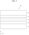
- FIG. 2 a photoelectric device according to some example embodiments is described with reference to FIG. 2 .
- FIG. 2 is a cross-sectional view showing a photoelectric device according to some example embodiments.
- a photoelectric device 200 includes a first electrode 10 and a second electrode 20 facing each other, and an active layer 30 between the first electrode 10 and the second electrode 20, like some example embodiments, including the example embodiments shown in FIG. 1 .
- the photoelectric device 200 according to some example embodiments, including the example embodiments shown in FIG. 2 further includes charge auxiliary layers 40 and 45 between the first electrode 10 and the active layer 30, and the second electrode 20 and the active layer 30, unlike some example embodiments, including the example embodiments shown in FIG. 1 .
- the charge auxiliary layers 40 and 45 may facilitate the transfer of holes and electrons separated from the active layer 30, so as to increase efficiency.
- the charge auxiliary layers 40 and 45 may be at least one selected from a hole injection layer (HIL) for facilitating hole injection, a hole transport layer (HTL) for facilitating hole transport, an electron blocking layer (EBL) for preventing electron transport, an electron injection layer (EIL) for facilitating electron injection, an electron transport layer (ETL) for facilitating electron transport, and a hole blocking layer (HBL) for preventing hole transport.
- HIL hole injection layer
- HTL hole transport layer
- EBL electron blocking layer
- EIL electron injection layer
- ETL electron transport layer
- HBL hole blocking layer
- the charge auxiliary layers 40 and 45 may include, for example, an organic material, an inorganic material, or an organic/inorganic material.
- the organic material may be an organic compound having hole or electron characteristics
- the inorganic material may be, for example, a metal oxide such as molybdenum oxide, tungsten oxide, nickel oxide, or the like.
- the hole injection layer (HIL) and/or hole transport layer (HTL) may include one selected from, for example, poly(3,4-ethylenedioxythiophene):poly(styrenesulfonate) (PEDOT:PSS), polyarylamine, poly(N-vinylcarbazole), polyaniline, polypyrrole, N,N,N',N'-tetrakis(4-methoxyphenyl)-benzidine (TPD), 4,4'-bis[N-(1-naphthyl)-N-phenyl-amino]biphenyl ( ⁇ -NPD), m-MTDATA, 4,4',4"-tris(N-carbazolyl)-triphenylamine (TCTA), or any combination thereof, but is not limited thereto.
- PEDOT:PSS poly(3,4-ethylenedioxythiophene):poly(styrenesulfonate)
- PDOT:PSS poly(styre
- the electron blocking layer may include one selected from, for example, poly(3,4-ethylenedioxythiophene):poly(styrenesulfonate) (PEDOT:PSS), polyarylamine, poly(N-vinylcarbazole), polyaniline, polypyrrole, N,N,N',N'-tetrakis(4-methoxyphenyl)-benzidine (TPD), 4,4'-bis[N-(1-naphthyl)-N-phenyl-amino]biphenyl ( ⁇ -NPD), m-MTDATA, 4,4',4"-tris(N-carbazolyl)-triphenylamine (TCTA), or any combination thereof, but is not limited thereto.
- the electron injection layer (EIL) and/or electron transport layer (ETL) may include one selected from, for example, 1,4,5,8-naphthalene-tetracarboxylic dianhydride (NTCDA), bathocuproine (BCP), LiF, Alq 3 , Gaq 3 , Inq 3 , Znq 2 , Zn(BTZ) 2 , BeBq 2 , or any combination thereof, but is not limited thereto.
- NTCDA 1,4,5,8-naphthalene-tetracarboxylic dianhydride
- BCP bathocuproine
- LiF LiF
- the hole blocking layer may include one selected from, for example, 1,4,5,8-naphthalene-tetracarboxylic dianhydride (NTCDA), bathocuproine (BCP), LiF, Alq 3 , Gaq 3 , Inq 3 , Znq 2 , Zn(BTZ) 2 , BeBq 2 , or any combination thereof, but is not limited thereto.
- NTCDA 1,4,5,8-naphthalene-tetracarboxylic dianhydride
- BCP bathocuproine
- LiF LiF
- Either one of the charge auxiliary layers 40 or 45 may be omitted.
- the photoelectric devices 100 and 200 may be applied to a solar cell, a light absorption sensor (e.g., an image sensor), a photo detector, an optical sensor, and a light emitting element, but is not limited thereto.
- a light absorption sensor e.g., an image sensor
- a photo detector e.g., an optical sensor
- a light emitting element e.g., a light emitting element
- an example of an image sensor including the organic photoelectric device is described referring to drawings.
- an image sensor also referred to herein as a light absorption sensor
- an organic CMOS image sensor according to some example embodiments is described, but it will be understood that the example embodiments are not limited thereto.
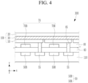
- FIG. 3 is a schematic top plan view showing an organic CMOS image sensor according to some example embodiments
- FIG. 4 is a cross-sectional view showing the organic CMOS image sensor of FIG. 3 .
- an organic CMOS image sensor 300 (which may also be referred to as a light absorption sensor) according to some example embodiments includes a semiconductor substrate 110 integrated with photo-sensing devices 50 (50B and 50R), which may be referred to as a blue photo-sensing device 50B and a red photo-sensing device 50R, a transmission transistor (not shown), a charge storage 55, a lower insulation layer 60, a color filter layer 70, an upper insulation layer 80, and a photoelectric device 100.
- the semiconductor substrate 110 may be a silicon substrate, and is integrated with the photo-sensing devices 50B and 50R, the transmission transistor (not shown), and the charge storage 55.
- the photo-sensing devices 50B and 50R may be photodiodes.
- the photo-sensing devices 50B and 50R, the transmission transistor, and/or the charge storage 55 may be integrated in each pixel, for example may be integrated in the semiconductor substrate 110 such that the photo-sensing devices 50B and 50R are located within a volume space defined by outermost surface of the semiconductor substrate 110 and may be at least partially exposed by the semiconductor substrate 110 or may be enclosed within an interior of the semiconductor substrate 110. As shown in the drawing, the photo-sensing devices 50B and 50R may be respectively included in a blue pixel and a red pixel and the charge storage 55 may be included in a green pixel.
- the blue photo-sensing device 50B may be configured to sense (e.g., selectively sense, including selectively absorbing and photoelectrically converting) blue light which is light in a blue wavelength region
- the red photo-sensing device 50R may be configured to sense (e.g., selectively sense, including selectively absorbing and photoelectrically converting) red light which is light in a red wavelength region.
- the photo-sensing devices 50B and 50R may be configured to sense (e.g., selectively sense) light, the information sensed by the photo-sensing devices 50B and 50R may be transferred by the transmission transistor, the charge storage 55 is electrically connected to the photoelectric device 100, and the information of the charge storage 55 may be transferred by the transmission transistor.
- the photo-sensing devices 50B and 50R are, for example, arranged in parallel without limitation, and the blue photo-sensing device 50B and the red photo-sensing device 50R may be stacked in a vertical direction.
- a metal wire (not shown) and a pad (not shown) are formed on the semiconductor substrate 110.
- the metal wire and pad may be made of a metal having low resistivity, for example, aluminum (Al), copper (Cu), silver (Ag), and alloys thereof, but are not limited thereto. Further, it is not limited to the structure, and the metal wire and pad may be positioned under the photo-sensing devices 50B and 50R.
- the lower insulation layer 60 is formed on the metal wire and the pad.
- the lower insulation layer 60 may be made of an inorganic insulating material such as a silicon oxide and/or a silicon nitride, or a low dielectric constant (low K) material such as SiC, SiCOH, SiCO, and SiOF.
- the lower insulation layer 60 has a trench exposing the charge storage 55. The trench may be filled with fillers.
- a color filter layer 70 is formed on the lower insulation layer 60.
- the color filter layer 70 includes a blue filter 70B formed in the blue pixel and configured to selectively transmit blue light and a red filter 70R formed in the red pixel and configured to selectively transmit red light.
- a cyan filter and a yellow filter may be disposed instead of the blue filter 70B and red filter 70R.
- a green filter is not included, but a green filter may be further included in some example embodiments.
- the color filter layer 70 may be omitted.
- the blue photo-sensing device 50B and the red photo-sensing device 50R may selectively absorb light in each wavelength region depending on their stack depth, and the color filter layer 70 may not be equipped.
- the upper insulation layer 80 is formed on the color filter layer 70.
- the upper insulation layer 80 eliminates a step caused by the color filter layer 70 and smoothens the surface.
- the upper insulation layer 80 and the lower insulation layer 60 may include a contact hole (not shown) exposing a pad, and a through-hole 85 exposing the charge storage 55 of the green pixel.
- the aforementioned photoelectric device 100 is formed on the upper insulation layer 80.
- the photoelectric device 100 includes the first electrode 10, the active layer 30, and the second electrode 20 as described above.
- the first electrode 10 and the second electrode 20 may be transparent electrodes, and the active layer 30 is the same as described above.
- the active layer 30 selectively absorbs and/or senses light in a green wavelength region and replaces a color filter of a green pixel.
- the light in a green wavelength region may be mainly absorbed in the active layer 30 and photoelectrically converted, while the light in the rest of the wavelength regions passes through first electrode 10 and may be sensed in the photo-sensing devices 50B and 50R.
- the photoelectric devices selectively absorbing light in a green wavelength region are stacked and thereby a size of an image sensor may be decreased and a down-sized image sensor may be realized.
- additional color filters may be further disposed on the photoelectric device 100.
- the additional color filters may include a blue filter 70B and a red filter 70R or a cyan filter and a yellow filter.
- FIG. 5 is a schematic cross-sectional view showing an organic CMOS image sensor according to some example embodiments.
- an organic CMOS image sensor 400 has the same structure as FIG. 4 except that a color filter layer 72 including the blue filter 72B and the red filter 72R is disposed on the photoelectric device 100 instead of a color filter layer 70 including the blue filter 70B and the red filter 70R disposed on the lower insulating layer 60.
- a cyan filter and a yellow filter may be disposed respectively.
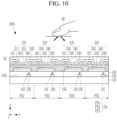
- FIG. 6 is a cross-sectional view showing an organic CMOS image sensor 500 to which the photoelectric device 200 is applied.
- the organic CMOS image sensor 500 includes a semiconductor substrate 110 integrated with photo-sensing devices 50B and 50R, a transmission transistor (not shown), and a charge storage 55, a lower insulation layer 60, and an upper insulation layer 80, like some example embodiments, including the example embodiments shown in FIG. 4 .
- the organic CMOS image sensor 500 includes the photoelectric device 200, unlike some example embodiments, including the example embodiments shown in FIG. 4 , which include the photoelectric device 100.
- FIG. 7 is a cross-sectional view showing an organic CMOS image sensor according to some example embodiments.
- the organic CMOS image sensor 600 includes a semiconductor substrate 110 integrated with photo-sensing devices 50B and 50R, a transmission transistor (not shown), and a charge storage 55, an insulation layer 80, and a photoelectric device 100, like some example embodiments, including the example embodiments illustrated in FIG. 4 .
- the organic CMOS image sensor 600 includes the blue photo-sensing device 50B and the red photo-sensing device 50R that are stacked in a vertical direction (e.g., perpendicular to a direction in which the upper surface of the semiconductor substrate 110 extends as shown in FIG. 7 ) in the semiconductor substrate 110 and does not include a color filter layer 70 and a lower insulation layer 60, unlike some example embodiments, including the example embodiments illustrated in FIG. 4 .
- the blue photo-sensing device 50B and the red photo-sensing device 50R are electrically connected with the charge storage 55, and the information of the charge storage 55 may be transferred by the transmission transistor (not shown).
- the blue photo-sensing device 50B and the red photo-sensing device 50R may selectively absorb light in each wavelength region depending on a stack depth.
- the photoelectric devices selectively absorbing light in a green wavelength region are stacked and the red photo-sensing device and the blue photo-sensing device are stacked, and thereby a size of an image sensor may be decreased and a down-sized image sensor may be realized.
- the photoelectric device 100 has improved green wavelength selectivity, and crosstalk caused by unnecessary absorption of light in a wavelength region except green may be decreased while increasing sensitivity.
- the photoelectric devices including an active layer 30 including the compound represented by Chemical Formula 1 may have improved photoelectric performance and/or reduced power consumption without compromising photoelectric conversion performance.
- the photoelectric device 100 of FIG. 1 is included, but it is not limited thereto, and thus the photoelectric device 200 of FIG. 2 may be applied in the same manner.
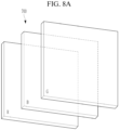
- FIG. 8A is a schematic view showing an organic CMOS image sensor according to some example embodiments and FIG. 8B is a cross-sectional view of the organic CMOS image sensor of FIG. 8A .
- the organic CMOS image sensor 700 includes a green photoelectric device (G) configured to selectively absorb light in a green wavelength region, a blue photoelectric device (B) configured to selectively absorb light in a blue wavelength region, and a red photoelectric device (R) configured to selectively absorb light in a red wavelength region that are stacked.
- G green photoelectric device
- B blue photoelectric device
- R red photoelectric device
- the organic CMOS image sensor 700 may include a green photoelectric device configured to selectively sense light in a green wavelength region, a blue photoelectric device configured to selectively sense light in a blue wavelength region, and a red photoelectric device configured to selectively sense light in a red wavelength region, where the green photoelectric device, the blue photoelectric device, and the red photoelectric device are stacked as shown in at least FIG. 8A .
- the photoelectric devices 100a to 100c may be stacked in a vertical direction on the semiconductor substrate 110, such that the photoelectric devices 100a to 100c at least partially overlap each other in a vertical direction that is perpendicular to an upper surface 110S of the semiconductor substrate 110, but example embodiments are not limited thereto.
- the organic CMOS image sensor 700 includes a semiconductor substrate 110, a lower insulation layer 60, an intermediate insulation layer 65, an upper insulation layer 80, a first device (i.e., photoelectric device, the same below) 100a, a second device 100b, and a third device 100c.
- a first device i.e., photoelectric device, the same below
- the semiconductor substrate 110 may be a silicon substrate, and a transmission transistor (not shown) and charge storages 155a, 155b, and 155c are integrated therein.
- Metal wires (not shown) and pads (not shown) are formed on the semiconductor substrate 110, and the lower insulation layer 60 is formed on the metal wires and the pads.
- the first device 100a, the second device 100b, and the third device 100c are sequentially formed on the lower insulation layer 60.
- any one of the first, second, or third devices 100a, 100b, or 100c may be the photoelectric devices 100 and/or 200 (e.g., a green photoelectric device according to some example embodiments) of FIG. 1 or 2 , and the other two of them (a red photoelectric device and a blue photoelectric device) may have the same structure as the photoelectric devices 100 and/or 200, but an active layer 30 therein may selectively absorb light in a red or blue wavelength region to photoelectrically convert the light.
- the first electrode 10 or the second electrode 20 of the photoelectric devices 100 and 200, the red photoelectric device and the blue photoelectric device may be connected to the charge storages 155a, 155b, and 155c.
- the active layer 30 of the first device 100a may selectively absorb light in any one wavelength region of red, blue, or green to photoelectrically convert the light.
- the first device 100a may be a red photoelectric conversion device configured to selectively sense light in a red wavelength region.
- the first electrode 10 or the second electrode 20 of the first device 100a may be electrically connected to the first charge storage 155a.
- a "photoelectric conversion device” may be interchangeably referred to herein as a "photoelectric device.”
- the intermediate insulation layer 65 may be formed on the first device 100a and the second device 100b may be formed on the intermediate insulation layer 65.
- the active layer 30 of the second device 100b may selectively absorb light in any one wavelength region of red, blue, or green to photoelectrically convert the light.
- the second device 100b may be a green photoelectric conversion device configured to selectively sense light in a green wavelength region.
- the second device 100b may be a blue photoelectric conversion device configured to selectively sense light in a blue wavelength region.
- the first electrode 10 or the second electrode 20 of the second device 100b may be electrically connected to the second charge storage 155b.
- the upper insulation layer 80 is formed on the second device 100b.
- the lower insulation layer 60, the intermediate insulation layer 65, and the upper insulation layer 80 have a plurality of through-holes 85a, 85b, and 85c exposing the charge storages 155a, 155b, and 155c.
- the third device 100c is formed on the upper insulation layer 80.
- the active layer 30 of the third device 100c may selectively absorb light in any one wavelength region of red, blue, or green to photoelectrically convert the light.
- the third device 100c may be a blue photoelectric conversion device configured to selectively sense light in a blue wavelength region.
- the third device 100c may be a green photoelectric conversion device configured to selectively sense light in a green wavelength region.
- the first electrode 10 or the second electrode 20 of the third device 100c may be electrically connected to the third charge storage 155c.
- a focusing lens (not shown) may be further formed on the third device 100c.
- the focusing lens may control direction of incident light and gather the light in one region.
- the focusing lens may have a shape of, for example, a cylinder or a hemisphere, but is not limited thereto.
- the first device 100a, the second device 100b, and the third device 100c that absorb light in different wavelength regions have a stacked structure, further reducing a size of the image sensor, implementing a down-sized image sensor, and simultaneously increasing sensitivity and reducing a crosstalk.
- the green photoelectric device, the blue photoelectric device, and the red photoelectric device are sequentially stacked, but the stack order may be changed without limitation.
- the green photoelectric device (G) may be the aforementioned photoelectric device 100 or photoelectric device 200
- the blue photoelectric device (B) may include electrodes facing each other and an active layer therebetween and including an organic material selectively absorbing light in a blue wavelength region
- the red photoelectric device (R) may include electrodes facing each other and an active layer therebetween and including an organic material selectively absorbing light in a red wavelength region.
- the green photoelectric device (G) configured to selectively absorb light in a green wavelength region
- the blue photoelectric device (B) configured to selectively absorb light in a blue wavelength region
- the red photoelectric device (R) configured to selectively absorb light in a red wavelength region
- the sensor-embedded display panel may be a display panel capable of performing a display function and a recognition function (e.g., biometric recognition function), and may be an in-cell type display panel in which a sensor performing a recognition function (e.g., biometric recognition function) is embedded in the display panel.
- a recognition function e.g., biometric recognition function
- FIG. 9 is a plan view illustrating an example of a sensor-embedded display panel according to some example embodiments and FIG. 10 is a cross-sectional view illustrating an example of a sensor-embedded display panel according to some example embodiments.
- a sensor-embedded display panel 1000 includes a plurality of subpixels PX's displaying different colors.
- the plurality of subpixels PX's may display at least three primary colors, for example, a first subpixel PX1, a second subpixel PX2, and a third subpixel PX3 displaying different first color, second color, and third color selected from red, green, and blue.
- the first color, the second color, and the third color may be red, green, and blue, respectively.
- the first subpixel PX1 may be a red subpixel displaying red
- the second subpixel PX2 may be a green subpixel displaying green
- the third subpixel PX3 may be a blue subpixel displaying blue.
- an auxiliary subpixel such as a white subpixel may be further included.
- Displaying a color may refer to emitting light corresponding to the color (e.g., light in a wavelength spectrum of the color).
- the sensor-embedded display panel 1000 may include a plurality of first subpixels PX1 configured to display a red color (e.g., light of a red wavelength spectrum) and including a first light emitting element (e.g., the first light emitting element 210 shown in FIG. 10 ), a plurality of second subpixels PX2 configured to display a green color (e.g., light of a green wavelength spectrum) and including a second light emitting element (e.g., the second light emitting element 220 shown in FIG.
- a red color e.g., light of a red wavelength spectrum
- a first light emitting element e.g., the first light emitting element 210 shown in FIG. 10
- a plurality of second subpixels PX2 configured to display a green color (e.g., light of a green wavelength spectrum) and including a second light emitting element (e.g., the second light emitting element 220 shown in FIG.
- third subpixels PX3 configured to display a blue color (e.g., light of a blue wavelength spectrum) and including a third light emitting element (e.g., the third light emitting element 230 shown in FIG. 10 ), where the first subpixels PX1, the second subpixels PX2, and the third subpixels PX3 are located in and/or at least partially define the display area DA.
- a blue color e.g., light of a blue wavelength spectrum
- a third light emitting element e.g., the third light emitting element 230 shown in FIG. 10
- the plurality of subpixels PX's including the first subpixel PX1, the second subpixel PX2, and the third subpixel PX3 may constitute (e.g., may define) one unit pixel UP to be arranged repeatedly along the row and/or column.
- a structure including one first subpixel PX1, two second subpixels PX2, and one third subpixel PX3 in the unit pixel UP is illustrated, but the inventive concepts are not limited thereto.
- At least one first subpixel PX1, at least one second subpixel PX2, and at least one third subpixel PX3 may be included.
- an arrangement of a Pentile type is illustrated, but the inventive concepts are not limited thereto.
- the subpixels PX's may be arranged variously.
- An area occupied by the plurality of subpixels PX's and displaying colors by the plurality of subpixels PX's may be a display area DA displaying an image.
- the area (e.g., in the xy plane) of the subpixels PX may collectively define the display area DA that is configured to display an image thereon (e.g., configured to display one or more colors).
- a portion of the area (e.g., in the xy plane) of the sensor-embedded display panel 1000 that excludes the display area DA may be a non-display area NDA that is configured to not display an image thereon (e.g., configured to not display any color).
- Each of the first subpixel PX1, the second subpixel PX2, and the third subpixel PX3 may include a light emitting element.
- the first subpixel PX1 may include a first light emitting element 210 capable of emitting light of a wavelength spectrum of a first color
- the second subpixel PX2 may include a second light emitting element 220 capable of emitting light of a wavelength spectrum of a second color
- the third subpixel PX3 may include a third light emitting element 230 capable of emitting light having a wavelength spectrum of a third color.
- the inventive concepts are not limited thereto, and at least one of the first subpixel PX1, the second subpixel PX2, or the third subpixel PX3 may include a light emitting element that emits light of a combination of a first color, a second color, and a third color, that is, light in a white wavelength spectrum, and may display a first color, a second color, or a third color through a color filter (not shown).
- a light emitting element that emits light of a combination of a first color, a second color, and a third color, that is, light in a white wavelength spectrum, and may display a first color, a second color, or a third color through a color filter (not shown).
- the terms “wavelength spectrum” and “wavelength region” may be used interchangeably.
- the sensor-embedded display panel 1000 includes the light absorption sensor 310.
- the light absorption sensor 310 may be disposed in a non-display area NDA.
- the non-display area NDA may be an area other than the display area DA, in which the first subpixel PX1, the second subpixel PX2, the third subpixel PX3, and optionally auxiliary subpixels are not arranged (e.g., a portion of the total area of the sensor-embedded display panel 1000 that excludes the display area DA, excludes the subpixels PX, is between adjacent subpixels PX, etc.).
- the area (e.g., in the xy plane) of the subpixels PX may collectively define the display area DA that is configured to display an image thereon (e.g., configured to display one or more colors).
- a portion of the area (e.g., in the xy plane) of the sensor-embedded display panel 1000 that excludes the display area DA e.g., portions of the area of the sensor-embedded display panel 1000 that are between adjacent subpixels PX in the xy direction, xy plane, etc.
- the light absorption sensor 310 may be disposed between at least two subpixels selected from the first subpixel PX1, the second subpixel PX2, and the third subpixel PX3 (e.g., between at least two subpixels of a first subpixel PX1 of a plurality of first subpixels PX1, a second subpixel PX2 of the plurality of second subpixels PX2, or a third subpixel PX3 of the plurality of third subpixels PX3), and may be disposed in parallel with the first, second, and third light emitting elements 210, 220, and 230 in the display area DA for example in parallel along the in-plane direction of the semiconductor substrate 110 (e.g., the xy direction as shown), which may be a direction extending parallel to an upper surface 110S of the semiconductor substrate 110.
- the third subpixel PX3 e.g., between at least two subpixels of a first subpixel PX1 of a plurality of first subpixels PX1, a second subpixel P
- the light absorption sensor 310 may be an optical type recognition sensor (e.g., biometric sensor).
- the light absorption sensor 310 may absorb light generated by reflection of light emitted from at least one of the first, second, or third light emitting elements 210, 220, or 230 disposed in the display area DA, by a recognition target 90 such as a living body, a tool, or a thing (e.g., may be configured to absorb light of a red wavelength spectrum, a green wavelength spectrum, a blue wavelength spectrum, an infrared wavelength spectrum, or any combination thereof), and then may convert it (the absorbed light) into an electrical signal.
- a recognition target 90 such as a living body, a tool, or a thing
- the living body may be a finger, a fingerprint, a palm, an iris, a face, and/or a wrist, but is not limited thereto.
- the light absorption sensor 310 may be, for example, a fingerprint sensor, an illumination sensor, an iris sensor, a distance sensor, a blood vessel distribution sensor, and/or a heart rate sensor, but is not limited thereto.
- the light absorption sensor 310 may be disposed on the semiconductor substrate 110 on the same plane as the first, second, and third light emitting elements 210, 220, and 230, and may be embedded in the sensor-embedded display panel 1000. Restated, the light absorption sensor 310 may be in parallel with the first, second, and third light emitting elements 210, 220, and 230 on the semiconductor substrate 110 along an in-plane direction of the semiconductor substrate 110. As described herein, the in-plane direction of the semiconductor substrate 110 may be a direction (e.g., the xy direction as shown) that extends in parallel with at least a portion of the semiconductor substrate 110, including an upper surface 110S of the semiconductor substrate 110.
- the sensor-embedded display panel 1000 includes a semiconductor substrate 110; a thin film transistor 120 disposed on the semiconductor substrate 110; an insulation layer 140 disposed on thin film transistor 120; a pixel definition layer 150 disposed on the insulation layer 140; and first, second, and third light emitting elements 210, 220, and 230 and the light absorption sensor 310 disposed in a space partitioned by the pixel definition layer 150.
- the semiconductor substrate 110 may be a light-transmitting substrate, for example, a glass substrate or a polymer substrate.
- the polymer substrate may include, for example, polycarbonate, polymethylmethacrylate, polyethyleneterephthalate, polyethylenenaphthalate, polyimide, polyamide, polyamideimide, polyethersulfone, polyorganosiloxane, a styrene-ethylene-butylene-styrene copolymer, polyurethane, polyacrylate, polyolefin, or any combination thereof, but is not limited thereto.
- a plurality of thin film transistors 120 are formed on the semiconductor substrate 110.
- One or more thin film transistor 120 may be included in each subpixel PX, and may include, for example, at least one switching thin film transistor and/or at least one driving thin film transistor.
- the semiconductor substrate 110 on which the thin film transistor 120 is formed may be referred to as a thin film transistor substrate (TFT substrate) or a thin film transistor backplane (TFT backplane).
- the insulation layer 140 may have a plurality of contact holes 141 for electrically connecting the first, second, and third light emitting elements 210, 220, and 230 and the thin film transistor 120 and a plurality of contact holes 142 for electrically connecting the light absorption sensor 310 and the thin film transistor 120.
- the insulation layer 140 may include an organic, inorganic, or organic-inorganic insulating material, in some example embodiments, an inorganic insulating material such as silicon oxide, silicon nitride, silicon oxynitride, aluminum oxide, aluminum nitride, or aluminum oxynitride; an organic insulating material such as polyimide, polyamide, polyamideimide, or polyacrylate; or an organic-inorganic insulating material such as polyorganosiloxane or polyorganosilazane.
- an inorganic insulating material such as silicon oxide, silicon nitride, silicon oxynitride, aluminum oxide, aluminum nitride, or aluminum oxynitride
- an organic insulating material such as polyimide, polyamide, polyamideimide, or polyacrylate
- an organic-inorganic insulating material such as polyorganosiloxane or polyorganosilazane.
- the pixel definition layer 150 may also be formed on the whole surface of the semiconductor substrate 110 and may be disposed between adjacent subpixels PX's to partition each subpixel PX.
- the pixel definition layer 150 may have a plurality of openings 151 disposed in each subpixel PX, and in each opening 151, any one of first, second, or third light emitting elements 210, 220, or 230 or the light absorption sensor 310 may be disposed.
- the pixel definition layer 150 be an insulation layer that may include an organic, inorganic, or organic-inorganic insulating material, in some example embodiments, an inorganic insulating material such as silicon oxide, silicon nitride, or silicon oxynitride; an organic insulating material such as polyimide; or an organic-inorganic insulating material such as polyorganosiloxane or polyorganosilazane.
- an inorganic insulating material such as silicon oxide, silicon nitride, or silicon oxynitride
- an organic insulating material such as polyimide
- an organic-inorganic insulating material such as polyorganosiloxane or polyorganosilazane.
- the first, second and third light emitting elements 210, 220, and 230 are formed on the semiconductor substrate 110 (or thin film transistor substrate), and are repeatedly arranged along the plane direction (e.g., xy direction) of the semiconductor substrate 110 (also referred to as an in-plane direction of the semiconductor substrate 110). As described above, the first, second, and third light emitting elements 210, 220, and 230 may be included in the first subpixel PX1, the second subpixel PX2, and the third subpixel PX3, respectively. The first, second, and third light emitting elements 210, 220, and 230 may be electrically connected to separate thin film transistors 120 and may be driven independently.
- the first, second and third light emitting elements 210, 220, and 230 may each independently emit one light selected from a red wavelength spectrum, a green wavelength spectrum, a blue wavelength spectrum, an infrared wavelength spectrum, or any combination thereof.
- the first light emitting element 210 may emit light of a red wavelength spectrum
- the second light emitting element 220 may emit light of a green wavelength spectrum
- the third light emitting element 230 may emit light of a blue wavelength spectrum.
- the red wavelength spectrum, the green wavelength spectrum, and the blue wavelength spectrum may have a maximum emission wavelength ( ⁇ max ) in a wavelength region of greater than about 600 nm and less than about 750 nm, about 500 nm to about 600 nm, and greater than or equal to about 400 nm and less than about 500 nm, respectively.
- ⁇ max maximum emission wavelength
- the first, second, and third light emitting elements 210, 220, and 230 may be, for example, light emitting diodes, for example, an organic light emitting diode including an organic material.
- the light absorption sensor 310 may be formed on the semiconductor substrate 110 (or the thin film transistor substrate), and may be randomly or regularly arranged along the plane direction (e.g., xy direction) of the semiconductor substrate 110. As described above, the light absorption sensor 310 may be disposed in the non-display area NDA, and may be connected to a separate thin film transistor 120 to be independently driven. The light absorption sensor 310 may absorb light of the same wavelength spectrum as the light emitted from at least one of the first, second, or third light emitting elements 210, 220, or 230 to convert it (the absorbed light) into an electrical signal.
- the light absorption sensor 310 may be, for example, a photoelectric diode, for example, an organic photoelectric diode including an organic material.
- Each of the first, second, and third light emitting elements 210, 220, and 230 and the light absorption sensor 310 may include separate, respective pixel electrodes 211, 221, 231, and 311; a separate portion of a common electrode 320 facing the pixel electrodes 211, 221, 231, and 311 and to which a common voltage is applied; and separate, respective light emitting layers 212, 222, and 232 or a light absorbing layer 330, a separate portion of a first common auxiliary layer 340, and a separate portion of a second common auxiliary layer 350 between the pixel electrodes 211, 221, 231, and 311 and the common electrode 320.
- the first, second, and third light emitting elements 210, 220, and 230 and the light absorption sensor 310 may be arranged in parallel along the plane direction (e.g., xy direction) of the semiconductor substrate 110, and the common electrode 320, the first common auxiliary layer 340, and the second common auxiliary layer 350 which are formed on the whole surface may be shared. For example, as shown in at least FIG.
- the light absorbing layer 330 of the light absorption sensor 310 and the light emitting layers 212, 222, and 232 of the first, second, and third light emitting elements 210, 220, and 230 may at least partially overlap with each other (e.g., partially or completely overlap each other) in the in-plane direction (e.g., xy direction) of the semiconductor substrate 110, which may be understood to be a horizontal direction that extends in parallel to an upper surface 110S of the semiconductor substrate 110 as shown in FIG.
- the light absorbing layer 330 and the light emitting layers 212, 222, and 232 may be at least partially positioned on the same plane (e.g., an xy plane extending in the xy directions that intersects each of the light absorbing layer 330 and the light emitting layers 212, 222, and 232).
- the common electrode 320 is continuously formed as a single piece of material that extends on the upper portion of the light emitting layers 212, 222, and 232 and the light absorbing layer 330, and is substantially formed on the whole surface of the semiconductor substrate 110.
- the common electrode 320 may apply a common voltage to the first, second, and third light emitting elements 210, 220, and 230 and the light absorption sensor 310.
- the first, second, and third light emitting elements 210, 220, and 230 and the light absorption sensor 310 may include separate portions of a single common electrode 320 that is a single piece of material that extends on each of the respective light emitting layers 212, 222, and 232 and the light absorbing layer 330 and between the first, second, and third light emitting elements 210, 220, and 230 and the light absorption sensor 310.
- the first common auxiliary layer 340 is disposed between the light emitting layers 212, 222, and 232 and light absorbing layer 330 and the common electrode 320 and may be continuously formed as a single piece of material that extends on the upper portions of the light emitting layers 212, 222, and 232 and the light absorbing layer 330 and on the lower portions of the common electrode 320.
- the first, second, and third light emitting elements 210, 220, and 230 and the light absorption sensor 310 may include separate portions of a single first common auxiliary layer 340 that is a single piece of material that extends on each of the respective light emitting layers 212, 222, and 232 and the light absorbing layer 330 and between the first, second, and third light emitting elements 210, 220, and 230 and the light absorption sensor 310.
- the first common auxiliary layer 340 is a charge auxiliary layer (e.g., electron auxiliary layer) that facilitates injection and/or movement of charges (e.g., electrons) from the common electrode 320 to the light emitting layers 212, 222, and 232.
- the LUMO energy level of the first common auxiliary layer 340 may be disposed between the LUMO energy levels of the light emitting layers 212, 222, and 232 and the work function of the common electrode 320, and the work function of the common electrode 320, the LUMO energy level of the first common auxiliary layer 340, and the LUMO energy levels of the light emitting layers 212, 222, and 232 may become shallow in sequence.
- the LUMO energy level of the first common auxiliary layer 340 may be shallower than the LUMO energy level of the light absorbing layer 330 and the work function of the common electrode 320, respectively.
- the first common auxiliary layer 340 may include an organic material, an inorganic material, an organic-inorganic material, or any combination thereof satisfying the LUMO energy level, for example a halogenated metal such as LiF, NaCl, CsF, RbCl, and Rbl; a lanthanide metal such as Yb; a metal oxide such as Li 2 O or BaO; Liq (lithium quinolate), Alq3 (tris(8-hydroxyquinolinato)aluminum), 1,3,5-tri[(3-pyridyl)-phen-3-yl]benzene, 2,4,6-tris (3'-(pyridin-3-yl)biphenyl-3-yl)-1,3,5-triazine, 2-(4-(N-phenylbenzoimidazolyl-1-ylphenyl)-9,10-dinaphthylanthracene, TPBi (1,3,5-tri(1-phenyl-1H-benzo[d]
- the second common auxiliary layer 350 may be disposed between the light emitting layers 212, 222, and 232 and the light absorbing layer 330 and the semiconductor substrate 110, and may be disposed between the light emitting layers 212, 222, and 232 and the light absorbing layer 330 and the pixel electrodes 211, 221, 231, and 311.
- the second common auxiliary layer 350 may be continuously formed as a single piece of material that extends on the lower portions of the light emitting layers 212, 222, and 232 and the light absorbing layer 330 and on the upper portions of pixel electrodes 211, 221, 231, and 311.
- the first, second, and third light emitting elements 210, 220, and 230 and the light absorption sensor 310 may include separate portions of a single second common auxiliary layer 350 that is a single piece of material that extends under each of the respective light emitting layers 212, 222, and 232 and the light absorbing layer 330 and between the first, second, and third light emitting elements 210, 220, and 230 and the light absorption sensor 310.
- the second common auxiliary layer 350 is a charge auxiliary layer (e.g., hole auxiliary layer) that facilitates injection and/or movement of charges (e.g., holes) from the pixel electrodes 211, 221, and 231 to the light emitting layers 212, 222, and 232.
- a charge auxiliary layer e.g., hole auxiliary layer
- the HOMO energy level of the second common auxiliary layer 350 may be disposed between the HOMO energy level of the light emitting layers 212, 222, and 232 and the work functions of the pixel electrodes 211, 221, and 231, and the work functions of the pixel electrodes 211, 221, and 231, the HOMO energy level of the second common auxiliary layer 350, and the HOMO energy levels of the light emitting layers 212, 222, and 232 may be sequentially deepened.
- the second common auxiliary layer 350 may include an organic material, an inorganic material, an organic-inorganic material, or any combination thereof satisfying the HOMO energy level, for example a phthalocyanine compound such as copper phthalocyanine; DNTPD (N,N'-diphenyl-N,N'-bis-[4-(phenyl-m-tolyl-amino)-phenyl]-biphenyl-4,4'-diamine), m-MTDATA (4,4',4"-[tris(3-methylphenyl)phenylamino] triphenylamine), TDATA (4,4'4"-tris(N,N-diphenylamino)triphenylamine), 2-TNATA (4,4',4"-tris(N-(2-naphthyl)-N-phenylamino)-triphenylamine), PEDOT/PSS (poly(3,4-ethylenedioxythiophene)/poly(4-styrenesul
- Each of the first, second, and third light emitting elements 210, 220, 230, and the light absorption sensor 310 includes a separate pixel electrode 211, 221, 231, or 311 facing the common electrode 320.
- One of the pixel electrodes 211, 221, 231, and 311 or the common electrode 320 is an anode and the other is a cathode.
- the pixel electrodes 211, 221, 231, and 311 may be an anode and the common electrode 320 may be a cathode.
- the pixel electrodes 211, 221, 231, and 311 are separated for each subpixel PX, and may be electrically connected to a separate thin film transistor 120 to be independently driven.
- the pixel electrodes 211, 221, 231, and 311 and the common electrode 320 may each be a light-transmitting electrode or a reflective electrode, and for example, at least one of the pixel electrodes 211, 221, 231, and 311 or the common electrode 320 may be a light-transmitting electrode.
- the light-transmitting electrode may be a transparent electrode or a semi-transmissive electrode.
- the transparent electrode may have a light transmittance of greater than or equal to about 85%, greater than or equal to about 90%, or greater than or equal to about 95% and the semi-transmissive electrode may have a light transmittance of greater than or equal to about 30% and less than about 85%, about 40% to about 80%, or about 40% to about 75%.
- the transparent electrode and the semi-transmissive electrode may include, for example, at least one of an oxide conductor, a carbon conductor, or a metal thin film.
- the oxide conductors may include, for example, one or more selected from indium tin oxide (ITO), indium zinc oxide (IZO), zinc tin oxide (ZTO), aluminum tin oxide (ATO), and aluminum zinc oxide (AZO), the carbon conductor may include one or more selected from graphene and carbon nanostructures, and the metal thin film may be a very thin film including aluminum (Al), magnesium (Mg), silver (Ag), gold (Au), magnesium-silver (Mg-Ag), magnesium-aluminum (Mg-Al), an alloy thereof, or any combination thereof.
- ITO indium tin oxide
- IZO indium zinc oxide
- ZTO zinc tin oxide
- ATO aluminum tin oxide
- AZO aluminum zinc oxide
- the carbon conductor may include one or more selected from graphene and carbon nanostructures
- the metal thin film may be a very thin film including aluminum (Al), magnesium (Mg), silver (Ag), gold (Au), magnesium-silver (M
- the reflective electrode may include a reflective layer having a light transmittance of less than or equal to about 5% and/or a reflectance of greater than or equal to about 80%, and the reflective layer may include an optically opaque material.
- the optically opaque material may include a metal, a metal nitride, or any combination thereof, for example silver (Ag), copper (Cu), aluminum (Al), gold (Au), titanium (Ti), chromium (Cr), nickel (Ni), an alloy thereof, a nitride thereof (e.g., TiN), or any combination thereof, but is not limited thereto.
- the reflective electrode may be formed of a reflective layer or may have a stacked structure of a reflective layer/transmissive layer or a transmissive layer/reflective layer/transmissive layer, and the reflective layer may be one layer or two or more layers.
- the sensor-embedded display panel 1000 may be a bottom emission type display panel that emits light toward the semiconductor substrate 110.
- the sensor-embedded display panel 1000 may be a top emission type display panel that emits light to the opposite side of the semiconductor substrate 110.
- the sensor-embedded display panel 1000 may be a both side emission type display panel.
- the pixel electrodes 211, 221, 231, and 311 may be reflective electrodes and the common electrode 320 may be a semi-transmissive electrode.
- the sensor-embedded display panel 1000 may have a microcavity structure. In the microcavity structure, reflection may occur repeatedly between the reflective electrode and the semi-transmissive electrode separated by a particular (or, alternatively, predetermined) optical length (e.g., a distance between the semi-transmissive electrode and the reflective electrode) and light of a particular (or, alternatively, predetermined) wavelength spectrum may be enhanced to improve optical properties.
- the sensor-embedded display panel 1000 may express colors with high color purity.
- light of a particular (or, alternatively, predetermined) wavelength spectrum may be repeatedly reflected between the semi-transmissive electrode and the reflective electrode to be modified.
- the modified light light having a wavelength spectrum corresponding to the resonance wavelength of a microcavity may be enhanced to exhibit photoelectric conversion characteristics amplified in a narrow wavelength region. Accordingly, the light absorption sensor 310 may exhibit high photoelectric conversion characteristics in a narrow wavelength region.
- Each of the first, second, and third light emitting elements 210, 220, and 230 includes light emitting layers 212, 222, and 232 between the pixel electrodes 211, 221, and 231 and the common electrode 320.
- Each of the light emitting layer 212 included in the first light emitting element 210, the light emitting layer 222 included in the second light emitting element 220, and the light emitting layer 232 included in the third light emitting element 230 may emit light in the same or different wavelength spectra and may emit light in, for example a red wavelength spectrum, a green wavelength spectrum, a blue wavelength spectrum, an infrared wavelength spectrum, or any combination thereof.
- the light emitting layer 212 may be a red light emitting layer that emits light in a red wavelength spectrum
- the light emitting layer 222 included in the second light emitting element 220 may be a green light emitting layer that emits light in a green wavelength spectrum
- the light emitting layer 232 included in the third light emitting element 230 may be a blue light emitting layer that emits light in a blue wavelength spectrum.
- the red wavelength spectrum, the green wavelength spectrum, and the blue wavelength spectrum may have a maximum emission wavelength in a wavelength region of greater than about 600 nm and less than about 750 nm, about 500 nm to about 600 nm, and greater than or equal to about 400 nm and less than about 500 nm, respectively.
- the light emitting layer of the white light emitting element may emit light of a full visible light wavelength spectrum, for example, light in a wavelength spectrum of greater than or equal to about 380 nm and less than about 750 nm, about 400 nm to about 700 nm, or about 420 nm to about 700 nm.
- the light emitting layers 212, 222, and 232 may include at least one host material and a fluorescent or phosphorescent dopant, and at least one of the at least one host material or the fluorescent or phosphorescent dopant may be an organic material.
- the organic material may include, for example, a low molecular weight organic material, such as a depositable organic material.
- the light emitting layers 212, 222, and 232 may include perylene; rubrene; 4-(dicyanomethylene)-2-methyl-6-[p-(dimethylamino)styryl]-4H-pyran; coumarin or a derivative thereof; carbazole or a derivative thereof; TPBi (2,2',2"-(1,3,5-benzenetriyl)-tris(1-phenyl-1-H-benzimidazole); TBADN (2-t-butyl-9,10-di(naphth-2-yl)anthracene); AND (9,10-di(naphthalene-2-yl)anthracene); CBP (4,4'-bis(N-carbazolyl)-1,1'-biphenyl); TCTA (4,4',4"-tris(carbazol-9-yl)-triphenylamine); DSA (distyrylarylene); CDBP (4,4'-bis(9
- the first, second, and third light emitting elements 210, 220, and 230 may be, for example, a quantum dot light emitting diode including quantum dots, or a perovskite light emitting diode including perovskite.
- the quantum dot may include, for example, a Group II-VI semiconductor compound, a Group III-V semiconductor compound, a Group IV-VI semiconductor compound, a Group IV semiconductor element or compound, a Group I-III-VI semiconductor compound, a Group I-II-IV-VI semiconductor compound, a Group II-III-V semiconductor compound, or any combination thereof.
- the Group II-IV semiconductor compound may be, for example, selected from a binary element semiconductor compound selected from CdSe, CdTe, ZnS, ZnSe, ZnTe, ZnO, HgS, HgSe, HgTe, MgSe, MgS, or a mixture thereof; a ternary element semiconductor compound selected from CdSeS, CdSeTe, CdSTe, ZnSeS, ZnSeTe, ZnSTe, HgSeS, HgSeTe, HgSTe, CdZnS, CdZnSe, CdZnTe, CdHgS, CdHgSe, CdHgTe, HgZnS, HgZnSe, HgZnTe, MgZnSe, MgZnS, or a mixture thereof; and a quaternary element semiconductor compound selected from HgZnTeS, CdZnSeS, CdZ
- the Group III-V semiconductor compound may be, for example, selected from a binary element semiconductor compound selected from GaN, GaP, GaAs, GaSb, AlN, AlP, AlAs, AlSb, InN, InP, InAs, InSb, or a mixture thereof; a ternary element semiconductor compound selected from GaNP, GaNAs, GaNSb, GaPAs, GaPSb, AlNP, AlNAs, AlNSb, AlPAs, AlPSb, InNP, InNAs, InNSb, InPAs, InPSb, or a mixture thereof; and a quaternary element semiconductor compound selected from GaAlNP, GaAlNAs, GaAlNSb, GaAlPAs, GaAlPSb, GaInNP, GaInNAs, GaInNSb, GaInPAs, GaInPSb, InAlNP, InAlNAs, InAlNSb, InAlPAs, InAlPSb, or a mixture thereof, but is not limited thereto.
- the Group IV-VI semiconductor compound may be, for example, selected from a binary element semiconductor compound selected from SnS, SnSe, SnTe, PbS, PbSe, PbTe, or a mixture thereof; a ternary element semiconductor compound selected from SnSeS, SnSeTe, SnSTe, PbSeS, PbSeTe, PbSTe, SnPbS, SnPbSe, SnPbTe, or a mixture thereof; and a quaternary element semiconductor compound selected from SnPbSSe, SnPbSeTe, SnPbSTe, or a mixture thereof, but is not limited thereto.
- the Group IV semiconductor element or compound may be, for example, selected from a semiconductor element such as Si, Ge, or a mixture thereof; and a binary element compound selected from SiC, SiGe, or a mixture thereof, but is not limited thereto.
- the Group I-III-VI semiconductor compound may be, for example, CuInSe 2 , CuInS 2 , CuInGaSe, CuInGaS, or a mixture thereof, but is not limited thereto.
- the Group I-II-IV-VI semiconductor compound may be, for example, CuZnSnSe, CuZnSnS, or a mixture thereof, but is not limited thereto.
- the Group II-III-V semiconductor compound may be, for example, InZnP, but is not limited thereto.
- the perovskite may be CH 3 NH 3 PbBr 3 , CH 3 NH 3 PbI 3 , CH 3 NH 3 SnBr 3 , CH 3 NH 3 SnI 3 , CH 3 NH 3 Sn 1-x Pb x Br 3 , CH 3 NH 3 Sn 1-x Pb x I 3 , HC(NH 2 ) 2 PbI 3 , HC(NH 2 ) 2 SnI 3 , (C 4 H 9 NH 3 ) 2 PbBr 4 , (C 6 H 5 CH 2 NH 3 ) 2 PbBr 4 , (C 6 H 5 CH 2 NH 3 ) 2 PbI 4 , (C 6 H 5 C 2 H 4 NH 3 ) 2 PbBr 4 , (C 6 H 13 NH 3 ) 2 (CH 3 NH 3 ) n-1 Pb n I 3n+1 (0 ⁇ x ⁇ 1 and n being any positive integer), or any combination thereof, but is not limited thereto.
- the light absorption sensor 310 includes a light absorbing layer 330 between the pixel electrode 311 and the common electrode 320.
- the light absorbing layer 330 is disposed in parallel with the light emitting layers 212, 222, and 232 of the first, second, and third light emitting elements 210, 220, and 230 along the plane direction (e.g., xy direction) of the semiconductor substrate 110.
- the light absorbing layer 330 and the light emitting layers 212, 222, and 232 may be disposed on the same plane.
- the light absorbing layer 330 may absorb light of a particular (or, alternatively, predetermined) wavelength spectrum and convert it into an electrical signal.
- the light absorbing layer 330 may absorb light generated by reflection of the aforementioned light emitted from at least one of the first, second, or third light emitting elements 210, 220, or 230, by the recognition target 90 and may convert it into an electrical signal.
- the light absorbing layer 330 may absorb light of a red wavelength spectrum, a green wavelength spectrum, a blue wavelength spectrum, an infrared wavelength spectrum, or any combination thereof.
- the light absorbing layer 330 may selectively absorb light of a red wavelength spectrum having a maximum absorption wavelength belonging to greater than about 600 nm and less than about 750 nm, and may absorb light generated by reflection of the light emitted from the red light emitting element among the first, second, and third light emitting elements 210, 220, and 230, by the recognition target 90.
- the light absorbing layer 330 may selectively absorb light of a green wavelength spectrum having a maximum absorption wavelength belonging to about 500 nm to about 600 nm, and may absorb light generated by reflection of the light emitted from the green light emitting element among the first, second and third light emitting elements 210, 220, and 230, by the recognition target 90.
- the light absorbing layer 330 may selectively absorb light in a blue wavelength spectrum having a maximum absorption wavelength belonging to greater than or equal to about 380 nm and less than about 500 nm, and may absorb light generated by reflection of the light emitted from the blue light emitting element among the first, second, and third light emitting elements 210, 220, and 230, by the recognition target 90.
- the light absorbing layer 330 may absorb light of a red wavelength spectrum, a green wavelength spectrum, and a blue wavelength spectrum, that is, light of a full visible wavelength spectrum of greater than or equal to about 380 nm and less than about 750 nm.
- the light absorbing layer 330 may absorb light generated by reflection of a combination of light emitted from the light emitting elements 210, 220, and 230, by the recognition target 90.
- the light absorbing layer 330 may include a p-type semiconductor and/or an n-type semiconductor for photoelectric conversion of the absorbed light.
- the p-type semiconductor and the n-type semiconductor may form a pn junction, generate excitons by receiving light from the outside, and then separate the generated excitons into holes and electrons.
- Each of the p-type semiconductor and the n-type semiconductor may be one or two or more, and the p-type semiconductor may be the compound represented by Chemical Formula 1.
- the light absorbing layer 330 may include the compound represented by Chemical Formula 1 as a p-type semiconductor and fullerene, a fullerene derivative, sub-phthalocyanine or a sub-phthalocyanine derivative, thiophene or a thiophene derivative, or the compound represented by Chemical Formula 6 as an n-type semiconductor.
- the n-type semiconductor may be represented by Chemical Formula 6A or 6B.
- the light absorbing layer 330 may be disposed in parallel with the light emitting layers 212, 222, and 232 along the plane direction (e.g., xy direction) of the semiconductor substrate 110 as described above, and may be disposed on the same plane as the light emitting layers 212, 222, and 232.
- the compound represented by Chemical Formula 1 may have an energy level capable of forming effective electrical matching with the first common auxiliary layer 340 as a p-type semiconductor of the light absorbing layer 330.
- a difference between the LUMO energy level of the first common auxiliary layer 340 and the LUMO energy level of the compound may be less than or equal to about 1.2 eV, and within the above range, less than or equal to about 1.1 eV, less than or equal to about 1.0 eV, less than or equal to about 0.8 eV, less than or equal to about 0.7 eV, less than or equal to about 0.5 eV, about 0 eV to about 1.2 eV, about 0 eV to about 1.1 eV, about 0 eV to about 1.0 eV, about 0 eV to about 0.8 eV, about 0 eV to about 0.7 eV, about 0 eV to about 0.5 eV, about 0.01 eV to about 1.2 eV,
- the light absorbing layer 330 may be an intrinsic layer (l layer) in which a p-type semiconductor and the n-type semiconductor are mixed in a bulk heterojunction form.
- the p-type semiconductor and the n-type semiconductor may be mixed in a volume ratio (or a thickness ratio) of about 1:9 to about 9:1, and within the above range, for example, about 2:8 to about 8:2, about 3:7 to about 7:3, about 4:6 to about 6:4, or about 5:5.
- a volume ratio or a thickness ratio
- the light absorbing layer 330 may include a p-type layer and an n-type layer instead of the intrinsic layer (I layer) or further include a p-type layer and/or an n-type layer on and/or under the intrinsic layer (I layer).
- the p-type layer may include, for example, a p-type semiconductor and the n-type layer may include an n-type semiconductor.
- the light absorbing layer 330 may be, for example, an I layer, a p-type layer/n-type layer, a p-type layer/I layer, an I layer/n-type layer, or a p-type layer/I layer/n-type layer, but is not limited thereto.
- the light emitting layers 212, 222, and 232 and the light absorbing layer 330 may each independently have a thickness of about 5 nm to about 300 nm, which may be about 10 nm to about 250 nm, about 20 nm to about 200 nm, or about 30 nm to about 180 nm within the above range.
- the difference between the thicknesses of the light emitting layers 212, 222, and 232 and the light absorbing layer 330 may be less than or equal to about 20 nm, within the above range, less than or equal to about 15 nm, less than or equal to about 10 nm, or less than or equal to about 5 nm.
- the light emitting layers 212, 222, and 232 and the light absorbing layer 330 may substantially have the same thickness.
- An encapsulation layer 95 may be formed on the first, second, and third light emitting elements 210, 220, and 230 and the light absorption sensor 310.
- the encapsulation layer 95 may include, for example, a glass plate, a metal thin film, an organic film, an inorganic film, an organic-inorganic film, or any combination thereof.
- the organic film may include, for example, an acrylic resin, a (meth)acrylic resin, polyisoprene, a vinyl resin, an epoxy resin, a urethane resin, a cellulose resin, a perylene resin, or any combination thereof, but is not limited thereto.
- the inorganic film may include, for example, oxides, nitrides and/or oxynitrides, for example silicon oxide, silicon nitride, silicon oxynitride, aluminum oxide, aluminum nitride, aluminum oxynitride, zirconium oxide, zirconium nitride, zirconium oxynitride, titanium oxide, titanium nitride, titanium oxynitride, hafnium oxide, hafnium nitride, hafnium oxynitride, tantalum oxide, tantalum nitride, tantalum oxynitride, or any combination thereof, but is not limited thereto.
- the organic-inorganic film may include, for example, polyorganosiloxane, but is not limited thereto.
- the encapsulation layer 95 may have one or two or more layers.
- the sensor-embedded display panel 1000 includes the first, second, and third light emitting elements 210, 220, and 230 for displaying colors by emitting light of a particular (or, alternatively, predetermined) wavelength spectrum, and the light absorption sensor 310 that absorbs the light generated by reflection of the light by the recognition target 90 and converts it into an electrical signal in the same plane on the semiconductor substrate 110, and thereby the display function and the recognition function (e.g., biometric recognition function) may be performed together.
- the display function and the recognition function e.g., biometric recognition function
- high performance slim-type sensor-embedded display panel 1000 may be implemented without increasing the thickness, unlike the conventional display panel in which a sensor is manufactured as a separate module and then is attached to the outside of the display panel or formed on the lower portion of the display panel.
- a recognition function e.g., a biometric recognition function
- a separate light source since there is no need to provide a separate light source outside the display panel, it is possible to prevent a decrease of the aperture ratio of the display panel due to the area occupied by the light source, and at the same time to save the power consumed by the separate light source, improving power consumption of the sensor-embedded display panel 1000.
- the first, second, and third light emitting elements 210, 220, and 230 and the light absorption sensor 310 share the common electrode 320, the first common auxiliary layer 340, and the second common auxiliary layer 350, and thereby the structure and process may be simplified compared to the case of forming the first, second, and third light emitting elements 210, 220, and 230 and the light absorption sensor 310 through separate processes.
- the light absorption sensor 310 may be an organic photoelectric diode including an organic light absorbing layer. Accordingly, it may have a light absorption that is twice or more higher than that of an inorganic diode such as a silicon photodiode and thus may have a high-sensitivity sensing function.
- the light absorbing layer 330 of the light absorption sensor 310 may include the compound represented by Chemical Formula 1, thereby selectively increasing the sensitivity to light in the green wavelength spectrum and improving color separation characteristics without mixing the absorption spectrum.
- the sensor-embedded display panel 1000 may additionally implement an anti-spoofing effect in addition to the aforementioned effect, and thus the color separation characteristics of the light reflected by the recognition target 90 may be improved, thereby further increasing the detail of the shape of the recognition target 90 and the color of the reflected light (e.g., skin color) may be selectively recognized, thereby further enhancing the accuracy of the biometric recognition function.
- the organic material included in the light absorbing layer 330 of the light absorption sensor 310 has a sublimation temperature difference within a particular (or, alternatively, predetermined) range with the organic materials of the light emitting layers 212, 222, and 232 of the first, second and third light emitting elements 210, 220, and 230, and thus deposition may be performed in the same process, thereby simplifying the process and increasing process stability.
- the light absorption sensor 310 may be disposed anywhere in the non-display area NDA (e.g., anywhere in a portion of the sensor-embedded display panel 1000 that does not vertically overlap (e.g., in the z direction) with any light emitting elements and thus is not configured to emit light and/or display color), a desired quantity of the light absorption sensors 310 may be disposed at one or more desired locations in the sensor-embedded display panel 1000.
- the biometric recognition function may be performed on any part of the screen of the electronic device such as a mobile device, and the biometric recognition function may be selectively performed at a specific location alone where the biometric recognition function is required according to the user's selection.
- FIG. 11 is a cross-sectional view illustrating another example of a sensor-embedded display panel according to some example embodiments.
- a sensor-embedded display panel 1000 includes a plurality of subpixels PX displaying different colors, that is, a first subpixel PX1, a second subpixel PX2, and a third subpixel PX3 displaying a first color, a second color, and a third color selected from red, green, and blue, and the first subpixel PX1, the second subpixel PX2, and the third subpixel PX3 include a first light emitting element 210, a second light emitting element 220, and a third light emitting element 230, respectively, like some example embodiments, including the example embodiments illustrated in FIGS. 9 and 10 .
- the sensor-embedded display panel 1000 may include the fourth light emitting element 240 that emits light in an infrared wavelength spectrum.
- the fourth light emitting element 240 may be included in the fourth subpixel PX4 adjacent to the first subpixel PX1, the second subpixel PX2, and/or the third subpixel PX3, or may be included in a non-display area, NDA.
- the fourth subpixel PX4 may form one unit pixel UP together with the first subpixel PX1, the second subpixel PX2, and the third subpixel PX3, and the unit pixel UP may be arranged repeatedly along rows and/or columns.
- the fourth light emitting element 240 is disposed on the semiconductor substrate 110 and may be disposed on the same plane as the first, second, and third light emitting elements 210, 220, and 230 and the light absorption sensor 310. For example, as shown in at least FIG.
- the light absorbing layer 330 of the light absorption sensor 310 and the light emitting layers 212, 222, 232, and 242 of the first, second, third, and fourth light emitting elements 210, 220, 230, and 240 may at least partially overlap with each other (e.g., partially or completely overlap each other) in the in-plane direction (e.g., xy direction) of the semiconductor substrate 110, which may be understood to be a horizontal direction that extends in parallel to an upper surface 110S of the semiconductor substrate 110 as shown in FIG.
- the light absorbing layer 330 and the light emitting layers 212, 222, 232, and 242 may be at least partially positioned on the same plane (e.g., an xy plane extending in the xy directions that intersects each of the light absorbing layer 330 and the light emitting layers 212, 222, 232, and 242).
- the fourth light emitting element 240 may be electrically connected to a separate thin film transistor 120 and driven independently.
- the fourth light emitting element 240 may have a structure in which the pixel electrode 241, the second common auxiliary layer 350, the light emitting layer 242, the first common auxiliary layer 340, and the common electrode 320 are sequentially stacked.
- the common electrode 320, the first common auxiliary layer 340, and the second common auxiliary layer 350 may be shared with the first, second, and third light emitting elements 210, 220, and 230, and the light absorption sensor 310.
- the light emitting layer 242 may emit light of an infrared wavelength spectrum, which may have for example a maximum emission wavelength in a range of greater than or equal to about 750 nm, about 750 nm to about 20 ⁇ m, about 780 nm to about 20 ⁇ m, about 800 nm to about 20 ⁇ m, about 750 nm to about 15 ⁇ m, about 780 nm to about 15 ⁇ m, about 800 nm to about 15 ⁇ m, about 750 nm to about 10 ⁇ m, about 780 nm to about 10 ⁇ m, about 800 nm to about 10 ⁇ m, about 750 nm to about 5 ⁇ m, about 780 nm to about 5 ⁇ m, about 800 nm to about 5 ⁇ m, about 750 nm to about 3 ⁇ m, about 780 nm to about 3 ⁇ m, about 800 nm to about 3 ⁇ m, about 750 nm to about 2 ⁇ m, about 780 n
- the light absorption sensor 310 may absorb light generated by reflection of light emitted from at least one of the first, second, third, or fourth light emitting elements 210, 220, 230, or 240, by a recognition target 90 such as a living body or a tool, and then convert it into an electrical signal.
- the light absorption sensor 310 may absorb light in an infrared wavelength spectrum generated by reflection of light emitted from the fourth light emitting element 240, by the recognition target 90, and then convert it into an electrical signal.
- the light absorbing layer 330 of the light absorption sensor 310 may include an organic material, an inorganic material, an organic-inorganic material, or any combination thereof that selectively absorbs light in the infrared wavelength spectrum.
- the light absorbing layer 330 may include a quantum dot, a quinoid metal complex compound, a polymethine compound, a cyanine compound, a phthalocyanine compound, a merocyanine compound, a naphthalocyanine compound, an immonium compound, a diimmonium compound, a triarylmethane compound, a dipyrromethene compound, an anthraquinone compound, a diquinone compound, a naphthoquinone compound, a squarylium compound, a rylene compound, a perylene compound, a squaraine compound, a pyrylium compound, a thiopyrylium compound, a diketopyrrolopyrrole compound, a boron dipyrromethene compound, a nickel-dithiol complex compound, a croconium compound, a derivative thereof, or any combination thereof, but is not limited thereto.
- the sensor-embedded display panel 1000 includes the fourth light emitting element 240 that emits light in the infrared wavelength spectrum and the light absorption sensor 310 that absorbs light in the infrared wavelength spectrum. Therefore, in addition to the recognition function (biometric recognition function), the sensitivity of the light absorption sensor 310 may be improved even in a low-illumination environment, and the detection capability of a 3D image may be further increased by widening a dynamic range for detailed division of black and white contrast. Accordingly, the sensing capability of the sensor-embedded display panel 1000 may be further improved.
- the light absorption sensor 310 may be provided separately from (e.g., independently of) a sensor-embedded display panel 1000 and/or from any light emitting elements, for example as a separate component of an electronic device.
- an electronic device such as the electronic device 2000 shown in FIG. 13 , may include a plurality of light absorption sensors 310, as a separate at least one additional device 1340, to serve as a camera for the electronic device separately from any light emitting elements and/or display panels of the electronic device 2000.
- first common auxiliary layer 340 and/or the second common auxiliary layer 350 may be absent from the sensor-embedded display panel 1000, and the light absorbing layer 330 may be understood to be between (e.g., directly between) a pair of electrodes (e.g., pixel electrode 211 and a portion of the common electrode 320).
- the common electrode 320 may be replaced by a plurality of separate pixel electrodes that are each included in a separate one of the light emitting elements 210, 220, 230, and/or 240 and/or the light absorption sensor 310 and may face a separate pixel electrode 211, 221, 231, and/or 241, and/or 311, such that the light absorbing layer 330 may be understood to be between (e.g., directly between) a pair of electrodes that include the pixel electrode 311 and a separate electrode included in the light absorption sensor 310.
- the aforementioned sensor-embedded display panel 1000 may be applied to (e.g., included in) electronic devices such as various display devices.
- Electronic devices such as display devices may be applied to, for example, mobile phones, video phones, smart phones, smart pads, smart watches, digital cameras, tablet PCs, laptop PCs, notebook computers, computer monitors, wearable computers, televisions, digital broadcasting terminals, e-books, personal digital assistants (PDAs), portable multimedia player (PMP), enterprise digital assistant (EDA), head mounted display (HMD), vehicle navigation, Internet of Things (IoT), Internet of all things (IoE), drones, door locks, safes, automatic teller machines (ATM), security devices, medical devices, or automotive electronic components, but are not limited thereto.
- PDAs personal digital assistants
- PMP portable multimedia player
- EDA enterprise digital assistant
- HMD head mounted display
- vehicle navigation Internet of Things
- IoT Internet of all things
- IoE Internet of all things
- drones door locks, safes, automatic teller
- FIG. 12 is a schematic view illustrating an example of a smart phone as an electronic device according to some example embodiments.
- the electronic device 2000 may include the aforementioned sensor-embedded display panel 1000, the sensor-embedded display panel 1000 having the light absorption sensor 310 disposed on the whole or a part of its area, and thus a biometric recognition function may be performed on any part of the screen, and according to the user's selection, the biometric recognition function may be selectively performed at a specific location alone where the biometric recognition function is required.
- An example of a method of recognizing the recognition target 90 in an electronic device 2000 such as a display device may include, for example, driving the first, second, and third light emitting elements 210, 220, and 230 of the sensor-embedded display panel 1000 (or the first, second, third, and fourth light emitting elements 210, 220, 230, and 240) and the light absorption sensor 310 to detect the light reflected by the recognition target 90 among the light emitted from the first, second, and third light emitting elements 210, 220, and 230 (or the first, second, third and fourth light emitting elements 210, 220, 230, and 240), in the light absorption sensor 310; comparing the image of the recognition target 90 stored in advance with the image of the recognition target 90 detected by the light absorption sensor 310; and judging the consistency of the compared images and if they match according to the determination that recognition of the recognition target 90 is complete, turning off the light absorption sensor 310, permitting user's access to the display device, and driving the
- FIG. 13 is a schematic view illustrating an example of a configuration diagram of an electronic device according to some example embodiments.
- the electronic device 2000 may further include a bus 1310, a processor 1320, a memory 1330, and at least one additional device 1340.
- Information of the aforementioned sensor-embedded display panel 1000, processor 1320, memory 1330, and at least one additional device 1340 may be transmitted to each other through the bus 1310.
- the at least one additional device 1340 may be omitted.
- the sensor-embedded display panel 1000 may be replaced by a display device including, for example, exclusively light emitting elements and no light absorption sensors, while the at least one additional device 1340 may include one or a plurality (e.g., an array) of photosensors according to any of the example embodiments which may serve as a biometric sensor, a camera, or the like.
- a display device including, for example, exclusively light emitting elements and no light absorption sensors
- the at least one additional device 1340 may include one or a plurality (e.g., an array) of photosensors according to any of the example embodiments which may serve as a biometric sensor, a camera, or the like.
- the processor 1320 may include one or more articles (e.g., units, instances, etc.) of processing circuitry such as a hardware including logic circuits; a hardware/software combination such as processor-implemented software; or any combination thereof.
- the processing circuitry may be a central processing unit (CPU), an arithmetic logic unit (ALU), a digital signal processor, a microcomputer, a field programmable gate array (FPGA), System-on-Chip (SoC), a programmable logic unit, a microprocessor, an application-specific integrated circuit (ASIC), and the like.
- the processing circuitry may include a non-transitory computer readable storage device.
- the processor 1320 may control, for example, a display operation of the sensor-embedded display panel 1000 or a sensor operation of the light absorption sensor 310.
- the memory 1330 may be a non-transitory computer readable storage medium, such as, for example, as a solid state drive (SSD) and may store an instruction program (e.g., program of instructions), and the processor 1320 may perform a function related to the sensor-embedded display panel 1000 by executing the stored instruction program.
- SSD solid state drive
- the at least one additional device 1340 may include one or more communication interfaces (e.g., wireless communication interfaces, wired interfaces), user interfaces (e.g., keyboard, mouse, buttons, etc.), power supply and/or power supply interfaces, or any combination thereof.
- communication interfaces e.g., wireless communication interfaces, wired interfaces
- user interfaces e.g., keyboard, mouse, buttons, etc.
- power supply and/or power supply interfaces e.g., power supply and/or power supply interfaces, or any combination thereof.
- the units and/or modules described herein may be implemented using hardware constituent elements and software constituent elements.
- the units and/or modules described herein may include, may be included in, and/or may be implemented by one or more articles of processing circuitry such as a hardware including logic circuits; a hardware/software combination such as processor-implemented software; or any combination thereof.
- the processing circuitry may be a central processing unit (CPU), an arithmetic logic unit (ALU), a digital signal processor, a microcomputer, a field programmable gate array (FPGA), System-on-Chip (SoC), a programmable logic unit, a microprocessor, an application-specific integrated circuit (ASIC), and the like.
- the hardware constituent elements may include microphones, amplifiers, band pass filters, audio-to-digital converters, and processing devices.
- the processing device may be implemented using one or more hardware devices configured to perform and/or execute program code by performing arithmetic, logic, and input/output operations.
- the processing device may include a processor, a controller and an arithmetic logic unit, a digital signal processor, a microcomputer, a field programmable array, a programmable logic unit, a microprocessor, or any other device capable of responding to and executing instructions.
- the processing device may access, store, operate, process, and generate data in response to execution of an operating system (OS) and one or more software running on the operating system.
- OS operating system
- the software may include a computer program, a code, an instruction, or any combination thereof, and may transform a processing device for a special purpose by instructing and/or configuring the processing device independently or collectively to operate as desired.
- the software and data may be implemented permanently or temporarily as signal waves capable of providing or interpreting instructions or data to machines, parts, physical or virtual equipment, computer storage media or devices, or processing devices.
- the software may also be distributed over networked computer systems so that the software may be stored and executed in a distributed manner.
- the software and data may be stored by one or more non-transitory computer readable storage devices.
- the method according to the foregoing example embodiments may be recorded in a non-transitory computer readable storage device including program instructions for implementing various operations of the aforementioned example embodiments.
- the storage device may also include program instructions, data files, data structures, and the like alone or in combination.
- the program instructions recorded in the storage device may be specially designed for some example embodiments or may be known to those skilled in computer software and available for use.
- Examples of non-transitory computer-readable storage devices may include magnetic media such as hard disks, floppy disks, and magnetic tapes; optical media such as CD-ROM discs, DVDs and/or blue-ray discs; magneto-optical media such as optical disks; and a hardware device configured to store and execute program instructions such as ROM, RAM, flash memory, and the like.
- the aforementioned device may be configured to operate as one or more software modules to perform the operations of the aforementioned example embodiments.
- a mixture of 1,4,5,8-naphthalenetetracarboxylic dianhydride (1 eq.) and 4-chloroaniline (2.2 eq.) is dissolved in a solvent of dimethyl formamide (DMF) and then, added to a two-necked and round-bottomed flask and stirred at 180 °C for 24 hours. Subsequently, after lowering the temperature to room temperature, methanol is added thereto to precipitate a product, which is filtered to obtain a powder-type material. The material is several times washed with methanol and then, purified by recrystallization with ethyl acetate and dimethylsulfoxide (DMSO).
- DMSO dimethylsulfoxide
- the compound represented by Chemical Formula 2-2 (made by Tokyo Chemical Industry) is purified through sublimation and may be used as an n-type semiconductor of a photoelectric device.
- Fullerene (C 60 , nanom purple ST, Frontier Carbon Corp.) is prepared and used as an N-type semiconductor of a photoelectric device.
- the compounds of Synthesis Examples 1-1 to 1-4 exhibit low reorganization energy of 0.091 eV to 0.162 eV, a DFT-calculated maximum absorption wavelength of 454.05 nm to 475.21 nm, and a corrected maximum absorption wavelength of 507.69 nm to 525.73 nm, which confirm absorption characteristics of a green wavelength region.
- the compounds of Comparative Synthesis Examples 1-1C and 1-2C exhibit high reorganization energy, and in addition, the compound of Comparative Synthesis Example 1-1C exhibits a longer maximum absorption wavelength than those of Synthesis Examples 1-1 to 1-4.
- the compounds of Synthesis Examples 1-1 to 1-4 exhibit polarizability of 500 bhor 3 or less, a dipole moment of 3 Debye or more, and oscillator strength of 0.8 or more and are expected to exhibit excellent electric characteristics and absorption coefficient.
- the compounds according to Synthesis Examples 1-1 to 1-4 are respectively deposited on a glass substrate, and energy levels of the deposited thin films (thickness: 15 nm) are measured.
- HOMO energy levels are evaluated with an amount of photoelectrons emitted by energy when irradiating UV light to a thin film using AC-2 (Hitachi) or AC-3 (Riken Keiki Co., Ltd.).
- Energy bandgaps are obtained by using a UV-Vis spectrometer (Shimadzu Corp.).
- LUMO energy levels are calculated by using the energy bandgaps and the HOMO energy levels. The results are shown in Table 3.
- the compounds according to Synthesis Example 1-1 to Synthesis Example 1-4 can be used as a p-type semiconductor.
- the sublimation temperature is evaluated through thermogravimetric analysis (TGA) from a temperature where a weight of a sample decreases by 10% relative to the initial weight by increasing the temperature under high vacuum (about 10 Pa or less).
- TGA thermogravimetric analysis
- the sublimation temperatures of the compounds according to the synthesis example is low, and thus the deposition stability thereof is improved.
- Example 1-1A Manufacture of Photoelectric Device
- Al (10 nm), ITO (100 nm), and Al (8 nm) are sequentially deposited on a glass substrate to form a lower electrode with an Al/ITO/Al structure (work function: 4.9 eV).
- N,N'-bis(3-methylphenyl)-N,N'-diphenyl-[1,1-biphenyl]-4,4'-diamine is deposited on the lower electrode to form a hole auxiliary layer (HOMO: 5.30 to 5.70 eV, LUMO: 2.00 to 2.30 eV).
- the compound represented by Chemical Formula 1-1 obtained in Synthesis Example 1-1 is deposited on the hole auxiliary layer at a rate of 0.25 ⁇ /s to form a p-type layer (10 nm), and the compound represented by Chemical Formula 2-1 according to Synthesis Example 2-1 is deposited at a rate of 0.25 ⁇ /s to form an n-type layer (40 nm), to form an active layer.
- 4,7-diphenyl-1,10-phenanthroline is deposited on the active layer to form an electron auxiliary layer (HOMO: 6.10 to 6.40 eV, LUMO: 2.90 to 3.20 eV).
- magnesium and silver are deposited on the electron auxiliary layer to form a Mg:Ag upper electrode to manufacture a photoelectric device (sensor).
- Each photoelectric device (sensor) according to Examples 1-2A to 1-4A is manufactured in the same manner as in Example 1-1A, except that each of the compounds represented by Chemical Formulas 1-2 to 1-4 according to Synthesis Examples 1-2 to 1-4 is used, instead of the compound represented by Chemical Formula 1-1 according to Synthesis Example 1-1.
- Each photoelectric device (sensor) according to Comparative Examples 1-1CA and 1-2CA is manufactured in the same manner as in Example 1-1A, except that the compound represented by Chemical Formula 1-1C or 1-2C according to Comparative Synthesis Example 1-1C or 1-2C is used, instead of the compound represented by Chemical Formula 1-1 according to Synthesis Example 1-1.
- Example 1-1B Manufacture of Photoelectric Device
- ITO is laminated on a glass substrate through sputtering to form an about 150 nm-thick anode, and the ITO glass substrate is ultrasonic wave-cleaned with acetone/isopropyl alcohol/pure water respectively for 15 minutes and then, UV ozone-cleaned. Subsequently, the compound according to Synthesis Example 1-1 and C60 are codeposited in a volume ratio of 1:1 to form a 100 nm-thick active layer, and ITO is vacuum-deposited to be 7 nm thick to manufacture a photoelectric device (sensor) having a structure of ITO (150 nm)/active layer (100 nm)/ITO (7 nm).
- Each photoelectric device (sensor) according to Examples 1-2B to 1-4B is manufactured in the same manner as in Example 1-1B, except that each of the compounds represented by Chemical Formulas 1-2 to 1-4 according to Synthesis Examples 1-2 to 1-4 is used, instead of the compound represented by Chemical Formula 1-1 according to Synthesis Example 1-1.
- Each photoelectric device (sensor) according to Comparative Examples 1-1CB and 1-2CB is manufactured in the same manner as in Example 1-1B, except that the compound represented by Chemical Formula 1-1C or 1-2C according to Comparative Synthesis Example 1-1C or 1-2C is used, instead of the compound represented by Chemical Formula 1-1 according to Synthesis Example 1-1.
- the external quantum efficiency (EQE) of the photoelectric devices according to Example 1-2A and Comparative Examples 1-1 CA and 1-2CA is evaluated at high temperature (85 °C).
- the external quantum efficiency (EQE) is evaluated by using incident photon to current efficiency (IPCE) at a wavelength of 450 nm (blue, B), 530 nm (green, G), and 630 nm (red, R).
- IPCE incident photon to current efficiency
- the photoelectric device according to Example 1-2A exhibits improved external quantum efficiency (photoelectric conversion efficiency) in the green wavelength spectrum compared to the photoelectric device according to Comparative Example 1-1CA or 1-2CA.
- the external quantum efficiency (EQE) of the photoelectric devices according to Example 1-2B and Comparative Examples 1-1CB and 1-2CB is evaluated at room temperature and high temperature (160 °C, 180 °C, and 190 °C).
- the external quantum efficiency (EQE) is evaluated by using incident photon to current efficiency (IPCE) at a wavelength of 450 nm (blue, B), 530 nm (green, G), and 630 nm (red, R).
- IPCE incident photon to current efficiency
- External quantum efficiency at high temperature is measured after leaving the photoelectric device at 160 °C, 180 °C, and 190 °C for 1 hour.
- the photoelectric device according to Example 1-2B exhibits improved external quantum efficiency (photoelectric conversion efficiency) in the green wavelength spectrum compared to the photoelectric device according to Comparative Example 1-1CB or 1-2CB.
- the photoelectric device of Example 1-2B exhibits a higher absorption coefficient (absorption intensity) than the photoelectric device of Comparative Examples 1-1CB and 1-2CB.
- an amount of the charges in the following frame is called to be an amount of remaining charges.
- the amount of the remaining charges is measured by irradiating light in the green wavelength region of 532 nm where the photoelectric conversion may occur for desired and/or alternatively predetermined time (40 sec), turning off the light, and integrating the current measured in units of 10 -6 seconds with an oscilloscope equipment, by time.
- the amount of the remaining charges is evaluated by a mA/cm 2 unit based on 5000 lux light. The results are shown in Table 7.
- the photoelectric device according to Example 1-2A has a lower number of remaining charges at room temperature and high temperature compared to the photoelectric device according to Comparative Example 1-2CA.
Landscapes
- Chemical & Material Sciences (AREA)
- Organic Chemistry (AREA)
- Physics & Mathematics (AREA)
- Engineering & Computer Science (AREA)
- Materials Engineering (AREA)
- Spectroscopy & Molecular Physics (AREA)
- Electromagnetism (AREA)
- General Physics & Mathematics (AREA)
- Theoretical Computer Science (AREA)
- Multimedia (AREA)
- Health & Medical Sciences (AREA)
- General Health & Medical Sciences (AREA)
- Vascular Medicine (AREA)
- Immunology (AREA)
- Pathology (AREA)
- Biochemistry (AREA)
- Analytical Chemistry (AREA)
- Life Sciences & Earth Sciences (AREA)
- Mathematical Physics (AREA)
- Plural Heterocyclic Compounds (AREA)
- Nitrogen Condensed Heterocyclic Rings (AREA)
- Electroluminescent Light Sources (AREA)
Applications Claiming Priority (1)
| Application Number | Priority Date | Filing Date | Title |
|---|---|---|---|
| KR20230025425 | 2023-02-24 |
Publications (1)
| Publication Number | Publication Date |
|---|---|
| EP4424689A1 true EP4424689A1 (fr) | 2024-09-04 |
Family
ID=90054098
Family Applications (1)
| Application Number | Title | Priority Date | Filing Date |
|---|---|---|---|
| EP24159360.7A Pending EP4424689A1 (fr) | 2023-02-24 | 2024-02-23 | Dérivés de 8,8-diméthyl-8h-thiéno[3',2':5,6]pyrido[3,2,1-jk]carbazole destinés à être utilisés dans des dispositifs photoélectriques |
Country Status (4)
| Country | Link |
|---|---|
| US (1) | US20240298535A1 (fr) |
| EP (1) | EP4424689A1 (fr) |
| KR (1) | KR20240132216A (fr) |
| CN (1) | CN118546157A (fr) |
Families Citing this family (2)
| Publication number | Priority date | Publication date | Assignee | Title |
|---|---|---|---|---|
| KR20230045272A (ko) * | 2021-09-28 | 2023-04-04 | 삼성전자주식회사 | 아민계 경화제 및 이를 포함하는 조성물, 반도체 패키지 및 전자 소자 |
| WO2026058896A1 (fr) * | 2024-09-11 | 2026-03-19 | 東ソー株式会社 | Élément électronique organique, matériau pour élément électronique organique et composé imide |
Citations (8)
| Publication number | Priority date | Publication date | Assignee | Title |
|---|---|---|---|---|
| WO2012143080A2 (fr) * | 2011-04-18 | 2012-10-26 | Merck Patent Gmbh | Matériaux pour dispositifs électroluminescents organiques |
| US20200194679A1 (en) * | 2017-09-11 | 2020-06-18 | Fujifilm Corporation | Photoelectric conversion element, optical sensor, imaging element, and compound |
| EP3848374A1 (fr) * | 2020-01-13 | 2021-07-14 | Samsung Electronics Co., Ltd. | Composé et dispositif photoélectrique, capteur d'image et dispositif électronique le comprenant |
| EP4006976A1 (fr) * | 2020-11-30 | 2022-06-01 | Samsung Electronics Co., Ltd. | Capteur d'image |
| US20220216418A1 (en) * | 2020-12-24 | 2022-07-07 | Samsung Electronics Co., Ltd. | Compound and photoelectric device, image sensor, and electronic device including the same |
| EP4124618A1 (fr) * | 2021-07-30 | 2023-02-01 | Samsung Electronics Co., Ltd. | Composé, dispositif photo-électrique, capteur d'absorption de lumière, panneau d'affichage intégré à un capteur et dispositif électronique |
| WO2023247338A1 (fr) * | 2022-06-20 | 2023-12-28 | Merck Patent Gmbh | Hétérocycles organiques pour dispositifs photoélectriques |
| EP4319537A1 (fr) * | 2022-08-02 | 2024-02-07 | Samsung Electronics Co., Ltd. | Photocapteur et panneau d'affichage intégré de capteur et dispositif électronique |
-
2024
- 2024-02-23 EP EP24159360.7A patent/EP4424689A1/fr active Pending
- 2024-02-23 KR KR1020240026827A patent/KR20240132216A/ko active Pending
- 2024-02-23 US US18/586,047 patent/US20240298535A1/en active Pending
- 2024-02-26 CN CN202410207623.XA patent/CN118546157A/zh active Pending
Patent Citations (8)
| Publication number | Priority date | Publication date | Assignee | Title |
|---|---|---|---|---|
| WO2012143080A2 (fr) * | 2011-04-18 | 2012-10-26 | Merck Patent Gmbh | Matériaux pour dispositifs électroluminescents organiques |
| US20200194679A1 (en) * | 2017-09-11 | 2020-06-18 | Fujifilm Corporation | Photoelectric conversion element, optical sensor, imaging element, and compound |
| EP3848374A1 (fr) * | 2020-01-13 | 2021-07-14 | Samsung Electronics Co., Ltd. | Composé et dispositif photoélectrique, capteur d'image et dispositif électronique le comprenant |
| EP4006976A1 (fr) * | 2020-11-30 | 2022-06-01 | Samsung Electronics Co., Ltd. | Capteur d'image |
| US20220216418A1 (en) * | 2020-12-24 | 2022-07-07 | Samsung Electronics Co., Ltd. | Compound and photoelectric device, image sensor, and electronic device including the same |
| EP4124618A1 (fr) * | 2021-07-30 | 2023-02-01 | Samsung Electronics Co., Ltd. | Composé, dispositif photo-électrique, capteur d'absorption de lumière, panneau d'affichage intégré à un capteur et dispositif électronique |
| WO2023247338A1 (fr) * | 2022-06-20 | 2023-12-28 | Merck Patent Gmbh | Hétérocycles organiques pour dispositifs photoélectriques |
| EP4319537A1 (fr) * | 2022-08-02 | 2024-02-07 | Samsung Electronics Co., Ltd. | Photocapteur et panneau d'affichage intégré de capteur et dispositif électronique |
Also Published As
| Publication number | Publication date |
|---|---|
| KR20240132216A (ko) | 2024-09-03 |
| US20240298535A1 (en) | 2024-09-05 |
| CN118546157A (zh) | 2024-08-27 |
Similar Documents
| Publication | Publication Date | Title |
|---|---|---|
| EP4124618B1 (fr) | Composé, dispositif photo-électrique, capteur d'absorption de lumière, panneau d'affichage intégré à un capteur et dispositif électronique | |
| EP4047661A2 (fr) | Panneau d'affichage intégré à un capteur et dispositif électronique | |
| EP4424689A1 (fr) | Dérivés de 8,8-diméthyl-8h-thiéno[3',2':5,6]pyrido[3,2,1-jk]carbazole destinés à être utilisés dans des dispositifs photoélectriques | |
| US12581853B2 (en) | Organic compound and sensor and sensor embedded display panel and electronic device | |
| US20240107881A1 (en) | Compound, photoelectric device, light absorption sensor, sensor embedded display panel, and electronic device | |
| US20230165046A1 (en) | Organic compound and sensor and sensor embedded display panel and electronic device | |
| US20240244965A1 (en) | Compound, photoelectric device, light absorption sensor, sensor embedded display panel, and electronic device | |
| US12559498B2 (en) | Organic compound, light absorption sensor, sensor-embedded display panel, and electronic device | |
| US20240321914A1 (en) | Compound, photoelectric device, light absorption sensor, sensor-embedded display panel, and electronic device | |
| US12612378B2 (en) | Compound, photoelectric device, light absorption sensor, sensor-embedded display panel, and electronic device | |
| US20240215275A1 (en) | Photoelectric device, light absorption sensor, sensor-embedded display panel, and electronic device | |
| US12439810B2 (en) | Compound, sensor, sensor embedded display panel, and electronic device | |
| US12358930B2 (en) | Compound and sensor and sensor embedded display panel and electronic device | |
| KR20240025474A (ko) | 화합물, 광전 소자, 흡광 센서, 센서 내장형 표시 패널 및 전자 장치 | |
| US12501830B2 (en) | Compound, sensor, sensor embedded display panel, and electronic device | |
| CN117586183A (zh) | 化合物、光电器件、光吸收传感器、传感器嵌入式显示面板和电子设备 | |
| EP4102574A1 (fr) | Panneau d'affichage à capteur intégré et dispositif électronique | |
| EP4714959A1 (fr) | Élément électroluminescent, composé polycyclique fusionné pour celui-ci et dispositif d'affichage le comprenant | |
| KR20230079300A (ko) | 유기 화합물, 센서, 센서 내장형 표시 패널 및 전자 장치 | |
| US20250185449A1 (en) | Sensor, image sensor, display panel, and device | |
| US20230157157A1 (en) | Light-emitting device including diamine-based compound, electronic apparatus including the light-emitting device, and the diamine-based compound | |
| EP4734730A1 (fr) | Élément électroluminescent, composé polycyclique condensé pour celui-ci et appareil électronique comprenant l'élément électroluminescent |
Legal Events
| Date | Code | Title | Description |
|---|---|---|---|
| PUAI | Public reference made under article 153(3) epc to a published international application that has entered the european phase |
Free format text: ORIGINAL CODE: 0009012 |
|
| STAA | Information on the status of an ep patent application or granted ep patent |
Free format text: STATUS: REQUEST FOR EXAMINATION WAS MADE |
|
| 17P | Request for examination filed |
Effective date: 20240326 |
|
| AK | Designated contracting states |
Kind code of ref document: A1 Designated state(s): AL AT BE BG CH CY CZ DE DK EE ES FI FR GB GR HR HU IE IS IT LI LT LU LV MC ME MK MT NL NO PL PT RO RS SE SI SK SM TR |
|
| RAP1 | Party data changed (applicant data changed or rights of an application transferred) |
Owner name: SAMSUNG DISPLAY CO., LTD. |
|
| STAA | Information on the status of an ep patent application or granted ep patent |
Free format text: STATUS: EXAMINATION IS IN PROGRESS |