EP4425568A1 - Dispositif à semi-conducteurs et son procédé de fabrication, et dispositif électronique - Google Patents
Dispositif à semi-conducteurs et son procédé de fabrication, et dispositif électronique Download PDFInfo
- Publication number
- EP4425568A1 EP4425568A1 EP21966607.0A EP21966607A EP4425568A1 EP 4425568 A1 EP4425568 A1 EP 4425568A1 EP 21966607 A EP21966607 A EP 21966607A EP 4425568 A1 EP4425568 A1 EP 4425568A1
- Authority
- EP
- European Patent Office
- Prior art keywords
- layer
- precursor
- gate
- titanium
- fin
- Prior art date
- Legal status (The legal status is an assumption and is not a legal conclusion. Google has not performed a legal analysis and makes no representation as to the accuracy of the status listed.)
- Pending
Links
Images




Classifications
-
- H—ELECTRICITY
- H10—SEMICONDUCTOR DEVICES; ELECTRIC SOLID-STATE DEVICES NOT OTHERWISE PROVIDED FOR
- H10D—INORGANIC ELECTRIC SEMICONDUCTOR DEVICES
- H10D30/00—Field-effect transistors [FET]
- H10D30/60—Insulated-gate field-effect transistors [IGFET]
-
- H—ELECTRICITY
- H10—SEMICONDUCTOR DEVICES; ELECTRIC SOLID-STATE DEVICES NOT OTHERWISE PROVIDED FOR
- H10D—INORGANIC ELECTRIC SEMICONDUCTOR DEVICES
- H10D30/00—Field-effect transistors [FET]
- H10D30/01—Manufacture or treatment
- H10D30/021—Manufacture or treatment of FETs having insulated gates [IGFET]
- H10D30/024—Manufacture or treatment of FETs having insulated gates [IGFET] of fin field-effect transistors [FinFET]
-
- H—ELECTRICITY
- H10—SEMICONDUCTOR DEVICES; ELECTRIC SOLID-STATE DEVICES NOT OTHERWISE PROVIDED FOR
- H10D—INORGANIC ELECTRIC SEMICONDUCTOR DEVICES
- H10D30/00—Field-effect transistors [FET]
- H10D30/60—Insulated-gate field-effect transistors [IGFET]
- H10D30/62—Fin field-effect transistors [FinFET]
-
- H—ELECTRICITY
- H10—SEMICONDUCTOR DEVICES; ELECTRIC SOLID-STATE DEVICES NOT OTHERWISE PROVIDED FOR
- H10D—INORGANIC ELECTRIC SEMICONDUCTOR DEVICES
- H10D48/00—Individual devices not covered by groups H10D1/00 - H10D44/00
- H10D48/30—Devices controlled by electric currents or voltages
-
- H—ELECTRICITY
- H10—SEMICONDUCTOR DEVICES; ELECTRIC SOLID-STATE DEVICES NOT OTHERWISE PROVIDED FOR
- H10D—INORGANIC ELECTRIC SEMICONDUCTOR DEVICES
- H10D64/00—Electrodes of devices having potential barriers
- H10D64/01—Manufacture or treatment
- H10D64/013—Manufacture or treatment of electrodes having a conductor capacitively coupled to a semiconductor by an insulator
- H10D64/01302—Manufacture or treatment of electrodes having a conductor capacitively coupled to a semiconductor by an insulator the insulator being formed after the semiconductor body, the semiconductor being silicon
- H10D64/01304—Manufacture or treatment of electrodes having a conductor capacitively coupled to a semiconductor by an insulator the insulator being formed after the semiconductor body, the semiconductor being silicon characterised by the conductor
- H10D64/01318—Manufacture or treatment of electrodes having a conductor capacitively coupled to a semiconductor by an insulator the insulator being formed after the semiconductor body, the semiconductor being silicon characterised by the conductor the conductor comprising a layer of alloy material, compound material or organic material contacting the insulator, e.g. TiN
-
- H—ELECTRICITY
- H10—SEMICONDUCTOR DEVICES; ELECTRIC SOLID-STATE DEVICES NOT OTHERWISE PROVIDED FOR
- H10D—INORGANIC ELECTRIC SEMICONDUCTOR DEVICES
- H10D64/00—Electrodes of devices having potential barriers
- H10D64/01—Manufacture or treatment
- H10D64/017—Manufacture or treatment using dummy gates in processes wherein at least parts of the final gates are self-aligned to the dummy gates, i.e. replacement gate processes
-
- H—ELECTRICITY
- H10—SEMICONDUCTOR DEVICES; ELECTRIC SOLID-STATE DEVICES NOT OTHERWISE PROVIDED FOR
- H10D—INORGANIC ELECTRIC SEMICONDUCTOR DEVICES
- H10D64/00—Electrodes of devices having potential barriers
- H10D64/60—Electrodes characterised by their materials
- H10D64/66—Electrodes having a conductor capacitively coupled to a semiconductor by an insulator, e.g. MIS electrodes
- H10D64/667—Electrodes having a conductor capacitively coupled to a semiconductor by an insulator, e.g. MIS electrodes the conductor comprising a layer of alloy material, compound material or organic material contacting the insulator, e.g. TiN workfunction layers
Definitions
- This application relates to the field of semiconductor technologies, and in particular, to a semiconductor chip, a production method therefor, and an electronic device.
- filling of a gate metal layer in a gate structure evolves from filling with aluminum (Al) by using a physical vapor deposition (Physical Vapor Deposition, PVD) method above 28 nm to filling with tungsten (W) by using a chemical vapor deposition (Chemical Vapor Deposition, CVD) method.
- PVD Physical Vapor Deposition
- W tungsten
- CVD chemical Vapor Deposition
- grinding fluid in a subsequent planarization process flows into a work function layer due to the existence of the gap in the gate metal layer, and as a result, changes electrical properties of the work function layer, affects a threshold voltage (Threshold voltage) of the device, and leads to drift of the threshold voltage.
- Theshold voltage threshold voltage
- This application provides a semiconductor chip, a production method therefor, and an electronic device, to implement seamless filling of a gate metal layer in a gate structure of the semiconductor chip.
- this application provides a semiconductor chip, including a substrate and a Fin FET located on the substrate, where the Fin FET includes a fin, a gate structure, and two sidewalls that are arranged opposite to each other.
- the fin generally includes a source, a drain, and a channel located between the source and the drain. Both the two sidewalls extend across the fin, and a trench is formed between the two sidewalls.
- the gate structure is located in the trench between the two sidewalls.
- the gate structure may include a gate dielectric layer and a gate metal layer that are stacked in sequence. In an implementation, the gate dielectric layer is formed on side surfaces and a bottom surface of the trench, and the gate metal layer fills a gap defined by the gate dielectric layer.
- the gate metal layer includes a titanium silicon nitride (TiSiN) layer.
- TiSiN titanium silicon nitride
- the gate metal layer includes only a TiSiN layer, that is, a TiSiN material is used to fill a gap, during filling with TiSiN, a lattice structure of TiN may be damaged due to doping of Si, so that a formed TiSiN thin film becomes an amorphous thin film. Because the amorphous thin film has a small grain size and low surface roughness, ahead-of-time sealing of a gap opening is prevented in nanometer scale due to an excessively large grain size.
- the gate metal layer including the TiSiN layer according to this application has an excellent gap filling capability, and can implement seamless filling with a high depth-width ratio.
- TiSiN with a low silicon concentration has a resistivity similar to or even lower than that of TiN. Therefore, a low-resistivity gate structure can be implemented, thereby improving a gate control speed of the semiconductor chip and enhancing high-frequency working stability of the semiconductor chip.
- the "depth-width ratio” refers to a ratio of a depth of a trench to a length of the trench in a channel direction.
- the high depth-width ratio in this application means that the ratio of a depth of a trench to a length of the trench in the channel direction is between 50:1 and 100:1.
- a plurality of film layers are "stacked" means that the plurality of film layers are formed layer by layer in a direction perpendicular to a surface of a base on which the plurality of film layers are to be formed.
- the gate structure is provided in the trench, the side surfaces and bottom of the trench are used as a base of the gate structure, and the gate dielectric layer and the gate metal layer in the gate structure being stacked means that the gate dielectric layer and the gate metal layer are formed layer by layer in a direction perpendicular to the side surfaces of the trench and a direction perpendicular to the bottom of the trench.
- the gate structure may further include a work function layer.
- the work function layer is located between the gate dielectric layer and the gate metal layer.
- the work function layer is formed on side surfaces and a bottom surface of the gate dielectric layer, and the gate metal layer fills a gap defined by the work function layer. Because the gate metal layer in this application can implement seamless filling, grinding fluid in a subsequent planarization process can be prevented from flowing into the work function layer, thereby preventing drift of a threshold voltage of the semiconductor chip.
- the work function layer is used for adjusting a work function value of the Fin FET, so that a formed transistor reaches an expected threshold voltage.
- the work function layer includes a P-type work function material, and the P-type work function material may be configured to have an expected work function value for use in a gate structure of the P-type field-effect transistor.
- the work function layer includes an N-type work function material, and the P-type work function material may be configured to have an expected work function value for use in a gate structure of the N-type field-effect transistor.
- the semiconductor chip may further include a first dielectric layer and a second dielectric layer.
- the first dielectric layer is located between the gate structure and the substrate and covers a surface of the substrate and a part of each side surface of the fin.
- the second dielectric layer is located above the first dielectric layer, and the second dielectric layer covers side surfaces and a top of the fin that are exposed at outer sides of the sidewalls. In other words, the second dielectric layer covers side surfaces and a top of the source and side surfaces and a top of the drain.
- the source and the drain are respectively located on two sides of two sidewalls, a channel is located between the source and the drain, and the gate structure covers a top and side surfaces of the channel.
- the gate dielectric layer is formed on the top and side surfaces of the channel, and is formed on side surfaces of the sidewalls and a part of a surface of the first dielectric layer.
- the work function layer is formed on side surfaces and an upper surface of the gate dielectric layer.
- the gate metal layer fills a gap defined by side surfaces and an upper surface of the work function layer.
- the percentage of atomic concentration can be obtained by scan analysis using a transmission electron microscope (Transmission Electron Microscope, TEM) and an energy dispersive spectrometer (Energy Dispersive Spectrometer, EDS) in combination.
- the percentage of atomic concentration can be obtained by scan analysis using a transmission electron microscope (Transmission Electron Microscope, TEM) and an energy dispersive spectrometer (Energy Dispersive Spectrometer, EDS) in combination.
- Si % + Ti % N %.
- the gate structure may further include a cover layer located between the gate dielectric layer and the work function layer as well as a barrier layer located between the cover layer and the work function layer.
- the gate dielectric layer covers the top and side surfaces of the channel
- the cover layer covers the side surfaces and the upper surface of the gate dielectric layer
- the barrier layer covers side surfaces and an upper surface of the cover layer
- the work function layer covers side surfaces and an upper surface of the barrier layer
- the gate metal layer fills the gap defined by the side surfaces and the upper surface of the work function layer.
- the cover layer is generally used for protecting quality of the gate dielectric layer from being affected by another subsequent process
- the barrier layer is generally used as an etching barrier layer of the work function layer.
- the cover layer may be formed by a deposition process by using a material such as titanium nitride (TiN) or TiSiN, and the barrier layer may be formed by a deposition process by using a material such as tantalum nitride (TaN).
- TiN titanium nitride
- TiSiN titanium nitride
- TaN tantalum nitride
- the gate dielectric layer may be formed by a deposition process such as chemical vapor deposition, plasma enhanced chemical vapor deposition, atomic layer deposition, or another suitable deposition process by using a material such as hafnium oxide (HfO 2 ), zirconium oxide (ZrO 2 ), hafnium zirconium oxide (HfZrO 2 ), aluminum oxide (Al 2 O 3 ), or silicon dioxide (SiO 2 ).
- a deposition process such as chemical vapor deposition, plasma enhanced chemical vapor deposition, atomic layer deposition, or another suitable deposition process by using a material such as hafnium oxide (HfO 2 ), zirconium oxide (ZrO 2 ), hafnium zirconium oxide (HfZrO 2 ), aluminum oxide (Al 2 O 3 ), or silicon dioxide (SiO 2 ).
- the gate dielectric layer may further include a dipole layer, where the dipole layer includes element lanthanum (La) and element aluminum (Al).
- the dipole layer includes element lanthanum (La) and element aluminum (Al).
- the work function layer is used for adjusting a work function value of the Fin FET, so that the formed transistor reaches an expected threshold voltage.
- the work function layer includes a P-type work function material, and the P-type work function material may be configured to have an expected work function value for use in a gate structure of the P-type field-effect transistor.
- the work function layer includes an N-type work function material, and the P-type work function material may be configured to have an expected work function value for use in a gate structure of the N-type field-effect transistor.
- the work function layer may be formed by using at least one material in titanium nitride (TiN), titanium aluminum carbide (TiAlC), titanium aluminum nitride (TiAlN), and TiSiN.
- TiN titanium nitride
- TiAlC titanium aluminum carbide
- TiAlN titanium aluminum nitride
- TiSiN TiSiN
- the work function layer may be formed by, for example, physical vapor deposition, chemical vapor deposition, plasma enhanced chemical vapor deposition, atomic layer deposition, or another suitable deposition process.
- the gate structure provided in embodiments of this application is applicable to both a short-channel FET and a long-channel FET.
- a TiSiN layer as a gate metal layer can not only implement gap-free filling, but also implement low resistivity of a gate structure.
- a gate metal layer may further include a metal filling layer located in a gap defined by a titanium silicon nitride layer.
- a process of the long-channel FET and a process of the short-channel FET can be both used, so that after the gate structure of the short-channel FET is formed, the metal filling layer continues to fill a trench of the long-channel FET, to complete production of the gate structure of the long-channel FET.
- a material of the metal filling layer may include tungsten, cobalt, or ruthenium, and is not limited herein.
- the short-channel FET means that a channel length of the FET is less than or equal to 30 nm
- the long-channel FET means that a channel length of the FET is greater than or equal to 100 nm.
- the channel length generally refers to the length of a channel in the direction from a source to a drain.
- the length of the trench in the channel direction limits the length of the gate structure, and the length of the gate structure is usually approximately equal to the length of the channel.
- both a short-channel Fin FET and a long-channel Fin FET may be provided.
- the semiconductor chip includes a first Fin FET and a second Fin FET, where the first Fin FET is a short-channel FET, and the second Fin FET is a long-channel FET.
- a channel length of the first Fin FET is less than or equal to 30 nm, and a channel length of the second Fin FET is greater than or equal to 100 nm.
- the channel length of the first Fin FET may be controlled to be between 18 nm and 30 nm, and the channel length of the second Fin FET may be controlled between 100 nm and 300 nm.
- a gate structure of the first Fin FET includes a gate dielectric layer, a work function layer, and a TiSiN layer.
- a gate structure of the second Fin FET includes a gate dielectric layer, a work function layer, a TiSiN layer, and a metal filling layer.
- gap-free filling of the gate metal layer is implemented by using the TiSiN layer
- gap-free filling of the gate metal layer is implemented by using the TiSiN layer and the metal filling layer.
- the TiSiN layer in the gate metal layer in the gate structure of the second Fin FET is formed by a same material as the TiSiN layer in the gate metal layer in the gate structure of the first Fin FET.
- the TiSiN layer in the gate metal layer of the second Fin FET and the TiSiN layer in the gate metal layer of the first Fin FET may be formed in a same process, thereby reducing process steps.
- a material of the metal filling layer in the gate metal layer may include tungsten, cobalt, or ruthenium, and is not limited herein.
- this application further provides an electronic device.
- the electronic device includes a circuit board and a semiconductor chip.
- the semiconductor chip is the semiconductor chip according to any one of the first aspect or the implementations of the first aspect.
- the semiconductor chip is electrically connected to the circuit board.
- a problem-resolving principle of the electronic device is similar to that of the foregoing semiconductor chip. Therefore, for implementation of the electronic device, refer to the implementation of the foregoing semiconductor chip. Details are not described herein again.
- this application further provides a semiconductor chip production method.
- the production method may include: forming, on a substrate, a fin and two sidewalls that extend across the fin and are arranged opposite to each other; next, forming a gate dielectric layer on side surfaces and a bottom surface of a trench defined by the two sidewalls; and finally forming a gate metal layer in a gap defined by the gate dielectric layer, where the gate metal layer includes a titanium silicon nitride layer.
- a work function layer may be further formed on side surfaces and a bottom surface of the gate dielectric layer, so that the gate metal layer is subsequently formed in the gap defined by the gate dielectric layer.
- a substrate on which the gate metal layer is to be formed may be placed in an atomic layer deposition chamber, a precursor of titanium and a precursor of nitrogen are alternately provided into the atomic layer deposition chamber, and a precursor of silicon is continuously provided into the atomic layer deposition chamber, to form a titanium silicon nitride layer in a gap defined by the work function layer.
- the substrate on which the gate metal layer is to be formed is placed in the atomic layer deposition chamber, and the titanium silicon nitride layer may be formed, through at least one process cycle, in the gap defined by the work function layer.
- One process cycle may include four stages T1 to T4. At stage T1, the precursor of titanium (Ti) is provided into the atomic layer deposition chamber.
- the precursor of Ti is removed from the atomic layer deposition chamber.
- the precursor of Ti may be removed from the atomic layer deposition chamber by gas extraction.
- the precursor of nitrogen (N) is provided into the atomic layer deposition chamber.
- the precursor of N is removed from the atomic layer deposition chamber.
- the precursor of N may be removed from the atomic layer deposition chamber by gas extraction.
- the precursor of Si is continuously provided into the atomic layer deposition chamber.
- T1 and T2 as well as T3 and T4 are exchangeable in sequence.
- stage T3 and stage T4 may be first performed before stage T1 and stage T2 are performed.
- a flow rate of the precursor of Si flowing into the atomic layer deposition chamber may be set to be less than or equal to 20% of that of the precursor of Ti, to ensure that content of Si in formed TiSiN is low.
- the precursor of Si flows in continuously. Because the precursor of Si is a reducing gas, if Cl exists in the precursor of Ti, the reducing gas that continuously flows in can effectively reduce Cl in the precursor of Ti, thereby reducing resistivity of the TiSiN layer.
- a substrate on which a gate metal layer is to be formed may be placed in an atomic layer deposition chamber, and a precursor of titanium, a precursor of nitrogen, and a precursor of silicon are provided into the atomic layer deposition chamber, to form a titanium silicon nitride layer in a gap defined by the work function layer.
- the TiSiN layer may be formed, through at least one process cycle, in the gap defined by the work function layer.
- One process cycle may include at least one first process sub-cycle P1 and one second process sub-cycle P2 after the at least one process sub-cycle.
- one first process sub-cycle P1 may include four stages T1 to T4.
- the precursor of Ti is provided into the atomic layer deposition chamber.
- the precursor of Ti is removed from the atomic layer deposition chamber.
- the precursor of Ti may be removed from the atomic layer deposition chamber by gas extraction.
- the precursor of N is provided into the atomic layer deposition chamber.
- the precursor of N is removed from the atomic layer deposition chamber by gas extraction.
- stage T3 and stage T4 may be first performed before stage T1 and stage T2 are performed.
- one second process sub-cycle P2 may include: providing the precursor of Si into the atomic layer deposition chamber.
- the "precursor” in this application is a precursor or a raw material for synthesizing a target substance (that is, TiSiN), that is, an atomic layer deposition reaction source.
- the precursor of Ti may include at least one of titanium tetrachloride (TiCl 4 ), tetrakis (dimethylamino)titanium (C 2 H 7 NTi, TDMAT), or tetrakis (diethylamido)titanium (C 16 H 40 N 4 Ti, TDEAT).
- the precursor of Si may include at least one of silane (SiH 4 ), disilane (Si 2 H 6 ), dichlorosilane (SiH 2 Cl, DCS), or hexachlorodisilane (Si 2 Cl 6 , HCD).
- the precursor of N may include at least one of ammonia (NH 3 ), nitrogen (N 2 ), nitrogen (N 2 )-H 2 plasma, NH 3 plasma, or N 2 plasma.
- duration of each stage in a process cycle needs to be configured based on an actual component and specific process conditions, and is not limited herein.
- the gate metal layer when the Fin FET to be formed is a short-channel FET, the gate metal layer includes only a TiSiN layer. In other words, the gap defined by the work function layer is completely filled with the TiSiN layer.
- forming the gate metal layer in the gap defined by the work function layer may further include: after a titanium silicon nitride layer is formed, forming a metal filling layer in the gap defined by the titanium silicon nitride layer. In other words, the gate metal layer includes the TiSiN layer and the metal filling layer.
- the semiconductor chip having a Fin FET provided in embodiments of this application, a gate structure is provided to cover a channel, so that ideal control of the channel can be implemented. Therefore, the semiconductor chip provided in embodiments of this application is widely applicable to various electronic devices, such as a logic device or a storage device. It should be noted that the semiconductor chip provided in embodiments of this application is intended to be used in electronic devices including but not limited to the foregoing electronic devices and any other electronic device of a suitable type.
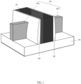
- FIG. 1 is a schematic diagram of a three-dimensional structure of a Fin FET. As shown in FIG. 1 , the Fin FET is disposed on a semiconductor substrate 01.
- the Fin FET includes a fin 02 provided on the semiconductor substrate 01, where the fin 02 includes a source 021, a drain 022, and a channel (not shown in FIG. 1 ) located between the source 021 and the drain 022; a gate structure 03 that extends across the fin 02 and covers a top and side surfaces of the channel; and two sidewalls 04 arranged opposite to each other on two sides of the gate structure 03.
- the gate structure 03 covers the top and the side surfaces on two sides of the channel, a drive current of the FET is increased, and device performance is improved.
- the gate structure is formed in a trench defined by the sidewalls, and the gate structure is usually formed by stacking a gate dielectric layer, a work function layer, and a tungsten filling layer.
- the gate length (the width of the trench) continuously decreases, and a gap formed in the tungsten filling layer causes high resistivity of the gate structure and low stability of a device.
- grinding fluid in a subsequent planarization process flows into the work function layer due to the existence of the gap in the tungsten filling layer, and as a result, changes electrical properties of the work function layer, and leads to a problem such as drift of the threshold voltage of the device.
- the gate structure is filled with aluminum titanium silicon nitride (TiAlN) instead of W.
- TiAlN titanium silicon nitride
- resistivity of TiAlN increases exponentially with an increase in content of aluminum (Al). Consequently, resistance of the gate structure increases, and a device rate decreases.
- particles are formed due to generation of an Al-C compound. This is not conducive to mass production.
- an embodiment of this application provides a gate structure that can reduce resistivity and implement seamless filling.
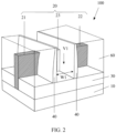
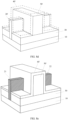
- FIG. 2 is a schematic diagram of a structure of a Fin FET in which no gate structure is provided according to an embodiment of this application.
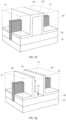
- FIG. 3 is a schematic diagram of a structure of the Fin FET shown in FIG. 2 in which a gate structure is provided.
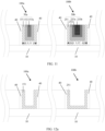
- FIG. 4a is a schematic diagram of a cross-sectional structure of the Fin FET shown in FIG. 3 in direction AA'.
- FIG. 4b is a schematic diagram of a cross-sectional structure of the Fin FET shown in FIG. 3 in direction BB'.
- a Fin FET 100 is provided on a substrate 10.
- the Fin FET 100 includes a fin 20, two sidewalls 40 that extend across the fin 20 and are arranged opposite to each other, and a gate structure 50 located in a trench V1 defined by the two sidewalls 40.
- the gate structure 50 may include: a gate dielectric layer 51 and a gate metal layer that are stacked in sequence.
- the gate metal layer includes a titanium silicon nitride (TiSiN) layer 53a.
- TiSiN titanium silicon nitride
- the gate dielectric layer 51 is formed on side surfaces and a bottom surface of the trench, and the gate metal layer fills a gap defined by the gate dielectric layer 51.
- the gate metal layer includes the TiSiN layer 53a, that is, a TiSiN material is used to fill the gap.
- the TiSiN layer in the gate structure provided in this application has an excellent gap filling capability, and can implement seamless filling of a gap with a high depth-width ratio (that is, a ratio of a depth of a trench to a length of the trench in a channel direction).
- the depth-width ratio is between 50:1 and 100:1.
- TiSiN with a low silicon concentration has a resistivity similar to or even lower than that of TiN. Therefore, a low-resistivity gate structure can be implemented, thereby improving a gate control speed of the semiconductor chip and enhancing high-frequency working stability of the semiconductor chip.
- a plurality of film layers are "stacked" means that the plurality of film layers are formed layer by layer in a direction perpendicular to a surface of a base on which the plurality of film layers are to be formed.
- the gate structure is provided in the trench, the side surfaces and bottom of the trench are used as a base of the gate structure, and the gate dielectric layer and the gate metal layer in the gate structure being stacked means that the gate dielectric layer and the gate metal layer are formed layer by layer in a direction perpendicular to the side surfaces of the trench and a direction perpendicular to the bottom of the trench.
- the gate structure 50 may further include a work function layer 52.
- the work function layer 52 is located between the gate dielectric layer 51 and the gate metal layer.
- the work function layer 52 is formed on side surfaces and a bottom surface of the gate dielectric layer 51, the gate metal layer fills a gap defined by the work function layer 52, and the gate metal layer is isolated from the gate dielectric layer 51 by the work function layer 52. Because the gate metal layer in this application can implement seamless filling, grinding fluid in a subsequent planarization process can be prevented from flowing into the work function layer, thereby preventing drift of a threshold voltage of the semiconductor chip.
- the work function layer is used for adjusting a work function value of the Fin FET, so that a formed transistor reaches an expected threshold voltage.
- the work function layer includes a P-type work function material, and the P-type work function material may be configured to have an expected work function value for use in a gate structure of the P-type field-effect transistor.
- the work function layer includes an N-type work function material, and the P-type work function material may be configured to have an expected work function value for use in a gate structure of the N-type field-effect transistor.
- the fin 20 usually includes a source 21, a drain 22, and a channel 23.
- the source 21 and the drain 22 are respectively located on two sides of the two sidewalls 40.
- the channel 23 is located between the source 21 and the drain 22.
- the gate structure 50 covers a top and side surfaces of the channel 23.
- the gate dielectric layer 51 is formed on the top and side surfaces of the channel 23, and is formed on side surfaces of the sidewalls 40 and a part of a surface of the first dielectric layer 30.
- the work function layer 52 is formed on side surfaces and an upper surface of the gate dielectric layer 51.
- the gate metal layer fills the gap defined by the side surfaces and the upper surface of the work function layer 52.
- a plurality of Fin FETs are usually formed on a substrate, and then the semiconductor chip needed is formed by cutting.
- fins in different Fin FETs usually need to be isolated by using a dielectric layer. Therefore, further, as shown in FIG. 2 and FIG. 3 , a first dielectric layer 30 and a second dielectric layer 60 are usually further provided in the semiconductor chip.
- the first dielectric layer 30 is located between the gate structure 50 and the substrate 10, and covers a surface of the substrate 10 and a part of each side surface of the fin 20.
- the second dielectric layer 60 is located above the first dielectric layer 30, and the second dielectric layer 60 covers side surfaces and a top of the fin 20 that are exposed at outer sides of the sidewalls 40. In other words, the second dielectric layer 60 covers side surfaces and a top of the source 21 and side surfaces and a top of the drain 22.
- the percentage of atomic concentration can be obtained by scan analysis using a transmission electron microscope (Transmission Electron Microscope, TEM) and an energy dispersive spectrometer (Energy Dispersive Spectrometer, EDS) in combination.
- the percentage of atomic concentration can be obtained by scan analysis using a transmission electron microscope (Transmission Electron Microscope, TEM) and an energy dispersive spectrometer (Energy Dispersive Spectrometer, EDS) in combination.
- Si % + Ti % N %.
- FIG. 5 is a schematic diagram of a cross-sectional structure of a gate structure according to an embodiment of this application.
- the gate structure 50 may further include a cover layer 54 located between the gate dielectric layer 51 and the work function layer 52 as well as a barrier layer 55 located between the cover layer 54 and the work function layer 52.
- the gate dielectric layer 51 covers the top and side surfaces of the channel 23.
- the cover layer 54 covers the side surfaces and upper surface of the gate dielectric layer 51.
- the barrier layer 55 covers side surfaces and an upper surface of the cover layer 54.
- the work function layer 52 covers side surfaces and an upper surface of the barrier layer 55.
- the gate metal layer fills the gap defined by the side surfaces and the upper surface of the work function layer 52.
- the cover layer 54 is generally used for protecting quality of the gate dielectric layer 51 from being affected by another subsequent process, and the barrier layer 55 is generally used as an etching barrier layer of the work function layer 52.
- the cover layer 54 may be formed by a deposition process by using a material such as titanium nitride (TiN) or TiSiN, and the barrier layer 55 may be formed by a deposition process by using a material such as tantalum nitride (TaN).
- the Fin FET provided in embodiments of this application is applicable to both a short-channel FET and a long-channel FET.
- a TiSiN layer as a gate metal layer can not only implement gap-free filling, but also implement low resistivity.
- FIG. 6 is a schematic diagram of a cross-sectional structure of another gate structure according to an embodiment of this application.
- the gate metal layer may further include a metal filling layer 53b located in a gap defined by a titanium silicon nitride layer 53a.
- a process of the long-channel FET and a process of the short-channel FET can be both used, so that after the gate structure of the short-channel FET is formed, the metal filling layer 53b continues to fill a trench of the long-channel FET, to complete production of the gate structure of the long-channel FET.
- a material of the metal filling layer may include tungsten, cobalt, or ruthenium, and is not limited herein.
- the short-channel FET means that a channel length of the FET is less than or equal to 30 nm
- the long-channel FET means that a channel length of the FET is greater than or equal to 100 nm.
- the channel length generally refers to the length of a channel in the direction from a source to a drain.
- a length W1 of the trench V1 in a direction of the channel 23 limits a length L1 of the gate structure 50, and the length L1 of the gate structure 50 is usually approximately equal to the length of the channel 23.
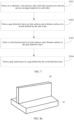
- FIG. 7 is a schematic flowchart of a semiconductor chip production method according to an embodiment of this application. As shown in FIG. 7 , the production method may include the following steps.
- Step S101 Form, on a substrate, a fin and two sidewalls that extend across the fin and are arranged opposite to each other.
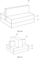
- An initial fin 20' is formed on the substrate 10, where the initial fin 20' may be formed by epitaxy on the substrate 10, or may be formed by etching the substrate 10. This is not limited herein.
- the substrate may be formed by a material such as silicon, a III-semiconductor material, an IV-semiconductor material, or a V-semiconductor material.
- the initial fin 20' may be formed by a semiconductor material such as Si, germanium (Ge), silicon germanium (SiGe), a III-semiconductor material, or a V-semiconductor material.
- a first dielectric layer 30 is formed on a surface of the substrate 10.
- a thickness of the first dielectric layer 30 is less than a thickness of the initial fin 20'.
- the first dielectric layer may be formed by deposition using a dielectric material such as one or a combination of silicon monoxide (SiO), silicon nitride (SiN), or silicon oxynitride (SiON).
- a dielectric material such as one or a combination of silicon monoxide (SiO), silicon nitride (SiN), or silicon oxynitride (SiON).
- a sacrificial gate 50' extending across the initial fin 20' is formed.
- the sacrificial gate 50' may be formed by deposition using a suitable material such as polycrystalline silicon or amorphous silicon. This is not limited herein.
- a sidewall material layer 40' (a film layer shown by a dashed line in FIG. 8d ) covering the sacrificial gate 50' and the first dielectric layer 30 is formed.
- the sidewall material layer may be formed by a dielectric material such as silicon monoxide (SiO), silicon nitride (SiN), or silicon oxynitride (SiON).
- a dielectric material such as silicon monoxide (SiO), silicon nitride (SiN), or silicon oxynitride (SiON).
- the sidewall material layer 40' located on two sides of the sacrificial gate 50' is generally referred to as sidewalls 40.
- a source 21 and a drain 22 are respectively formed in a source region and a drain region of the initial fin 20'.
- a part of the initial fin 20' located between the source 21 and the drain is a channel 23.
- the source 21, the drain 22, and the channel 23 are generally collectively referred to as a fin.
- the source and the drain may be formed by an ion implantation process, or may be formed by epitaxy. This is not limited herein.
- the second dielectric layer may be formed by SiO, SiN, SiON, or another dielectric material.
- the sacrificial gate 50' and the sidewall material layer 40' located on the sacrificial gate 50' are removed, so that a trench V1 is formed between the two sidewalls 40, and the channel 23 is exposed.
- the forming a gate structure in the trench may include the following steps.
- Step S102 As shown in FIG. 8h , form a gate dielectric layer 51 on side surfaces and a bottom surface of the trench defined by the sidewalls 40.
- the gate dielectric layer may be formed by a deposition process such as chemical vapor deposition, plasma enhanced chemical vapor deposition, atomic layer deposition, or another suitable deposition process by using a material such as hafnium oxide (HfO 2 ), zirconium oxide (ZrO 2 ), hafnium zirconium oxide (HfZrO 2 ), aluminum oxide (Al 2 O 3 ), or silicon dioxide (SiO 2 ).
- a deposition process such as chemical vapor deposition, plasma enhanced chemical vapor deposition, atomic layer deposition, or another suitable deposition process by using a material such as hafnium oxide (HfO 2 ), zirconium oxide (ZrO 2 ), hafnium zirconium oxide (HfZrO 2 ), aluminum oxide (Al 2 O 3 ), or silicon dioxide (SiO 2 ).
- the gate dielectric layer may further include a dipole layer, where the dipole layer includes element lanthanum (La) and element aluminum (Al).
- the dipole layer includes element lanthanum (La) and element aluminum (Al).
- step S103 may further be included.
- a work function layer 52 is formed on side surfaces and a bottom surface of the gate dielectric layer 51.
- the work function layer may be formed by using at least one material in titanium nitride (TiN), titanium aluminum carbide (TiAlC), titanium aluminum nitride (TiAlN), and TiSiN.
- TiN titanium nitride
- TiAlC titanium aluminum carbide
- TiAlN titanium aluminum nitride
- TiSiN TiSiN
- the work function layer may be formed by, for example, physical vapor deposition, chemical vapor deposition, plasma enhanced chemical vapor deposition, atomic layer deposition, or another suitable deposition process.
- Step S104 As shown in FIG. 8j , form a gate metal layer in a gap defined by the work function layer 52, where the gate metal layer includes a TiSiN layer 53a.
- a substrate on which the gate metal layer is to be formed may be placed in an atomic layer deposition chamber, a precursor of titanium and a precursor of nitrogen are alternately provided into the atomic layer deposition chamber, and a precursor of silicon is continuously provided into the atomic layer deposition chamber, to form a titanium silicon nitride layer in the gap defined by the work function layer.
- the substrate on which the gate metal layer is to be formed is placed in the atomic layer deposition chamber, and the TiSiN layer may be formed, through at least one process cycle, in the gap defined by the work function layer.
- FIG. 9 is a sequence diagram of a process cycle during forming of a TiSiN layer according to this application. As shown in FIG. 9 , one process cycle may include four stages T1 to T4.
- a first precursor and a precursor of silicon (Si) are provided into an atomic layer deposition chamber.
- the "precursor” in this application is a precursor or a raw material for synthesizing a target substance (that is, TiSiN), that is, an atomic layer deposition reaction source.
- the first precursor may be a precursor of titanium (Ti) or a precursor of nitrogen (N).
- Ti titanium
- N nitrogen
- FIG. 9 an example in which the first precursor is a precursor of Ti is used for illustration.
- the precursor of Ti may include at least one of titanium tetrachloride (TiCl 4 ), tetrakis (dimethylamino)titanium (C 2 H 7 NTi, TDMAT), or tetrakis (diethylamido)titanium (C 16 H 40 N 4 Ti, TDEAT).
- TiCl 4 titanium tetrachloride
- TDMAT tetrakis (diethylamido)titanium
- TDEAT tetrakis (diethylamido)titanium
- the precursor of N may include at least one of ammonia (NH 3 ), nitrogen (N 2 ), nitrogen (N 2 )-H 2 plasma, NH 3 plasma, or N 2 plasma.
- the precursor of Si may include at least one of silane (SiH 4 ), disilane (Si 2 H 6 ), dichlorosilane (SiH 2 Cl, DCS), or hexachlorodisilane (Si 2 Cl 6 , HCD).
- the precursor of Si is provided into the atomic layer deposition chamber, and the first precursor is removed from the atomic layer deposition chamber.
- the first precursor may be removed from the atomic layer deposition chamber by gas extraction.
- a second precursor and the precursor of Si are provided into the atomic layer deposition chamber.
- the second precursor may be a precursor of N or a precursor of Ti.
- the second precursor is a precursor of N is used for illustration.
- the precursor of Si is provided into the atomic layer deposition chamber, and the second precursor is removed from the atomic layer deposition chamber.
- the second precursor may be removed from the atomic layer deposition chamber by gas extraction.
- stage T1 to stage T4 the precursor of Si needs to be continuously provided into the atomic layer deposition chamber.
- a peak indicates that the precursor is provided into the atomic layer deposition chamber
- a valley indicates that the precursor is not provided into the atomic layer deposition chamber.
- a peak indicates that gas extraction is performed
- a valley indicates that gas extraction is not performed.
- duration of each stage in a process cycle needs to be configured based on an actual component and specific process conditions, and is not limited herein.
- Duration T1 to duration T4 in FIG. 9 are merely used for illustration, and are not specifically limited herein.
- a flow rate of the precursor of Si flowing into the atomic layer deposition chamber may be set to be less than or equal to 20% of that of the precursor of Ti, to ensure that content of Si in formed TiSiN is low.
- the precursor of Si flows in continuously. Because the precursor of Si is a reducing gas, if Cl exists in the precursor of Ti, the reducing gas that continuously flows in can effectively reduce Cl in the precursor of Ti, thereby reducing resistivity of the TiSiN layer.
- a substrate on which a gate metal layer is to be formed may be placed in an atomic layer deposition chamber, and a precursor of titanium, a precursor of nitrogen, and a precursor of silicon are provided into the atomic layer deposition chamber, to form a titanium silicon nitride layer in a gap defined by the work function layer.
- the TiSiN layer may be formed, through at least one process cycle, in the gap defined by the work function layer.
- FIG. 10 is a sequence diagram of a process cycle during forming of a TiSiN layer according to this application.
- one process cycle may include at least one first process sub-cycle P1 and one second process sub-cycle P2 after the at least one process sub-cycle P1.
- FIG. 10 an example in which one process cycle includes two P1 and one P2 is used for illustration.
- one first process sub-cycle P1 may include four stages T1 to T4.
- a first precursor is provided into the atomic layer deposition chamber.
- the first precursor may be a precursor of titanium (Ti) or a precursor of nitrogen (N).
- Ti titanium
- N nitrogen
- FIG. 10 an example in which the first precursor is a precursor of Ti is used for illustration.
- the precursor of Ti may include at least one of TiCl 4 , C 2 H 7 NTi (TDMAT), or C 16 H 40 N 4 Ti (TDEAT).
- the precursor of N may include at least one of NH 3 , N 2 , N 2 -H 2 plasma, NH 3 plasma, or N 2 plasma.
- the first precursor is removed from the atomic layer deposition chamber.
- the first precursor may be removed from the atomic layer deposition chamber by gas extraction.
- a second precursor is provided into the atomic layer deposition chamber.
- the second precursor may be a precursor of N or a precursor of Ti.
- the second precursor is a precursor of N is used for illustration.
- the second precursor is removed from the atomic layer deposition chamber.
- the second precursor may be removed from the atomic layer deposition chamber by gas extraction.
- one second process sub-cycle P2 may include: providing a precursor of Si into the atomic layer deposition chamber.
- the precursor of Si may include at least one of SiH 4 , Si 2 H 6 , SiH 2 Cl (DCS), or Si 2 Cl 6 (HCD).
- a peak indicates that the precursor is provided into the atomic layer deposition chamber
- a valley indicates that the precursor is not provided into the atomic layer deposition chamber.
- a peak indicates that gas extraction is performed
- a valley indicates that gas extraction is not performed.
- duration of each stage in a process cycle needs to be configured based on an actual component and specific process conditions, and is not limited herein. Duration of T1 to T4 and P2 in FIG. 10 is merely used for illustration, and does not specifically constitute a limitation on duration.
- the gate metal layer includes only a TiSiN layer. In other words, the gap defined by the work function layer is completely filled with the TiSiN layer.
- forming the gate metal layer in the gap defined by the work function layer may further include: after a titanium silicon nitride layer is formed, forming a metal filling layer in the gap defined by the titanium silicon nitride layer.
- the gate metal layer includes the TiSiN layer and the metal filling layer.
- film layers such as the gate dielectric layer, the work function layer, and the gate metal layer in the gate structure are further formed on a surface of the second dielectric layer. Therefore, after filling of the gate metal layer is completed, the gate metal layer, the work function layer, and the gate dielectric layer that are located above the second dielectric layer further need to be removed by a chemical mechanical polishing (Chemical Mechanical Polishing, CMP) process, so that only the gate dielectric layer, the work function layer, and the gate metal layer in the trench are retained.
- CMP Chemical Mechanical Polishing
- FIG. 11 is a schematic diagram of a cross-sectional structure of a semiconductor chip according to an embodiment of this application.
- the semiconductor chip includes a first Fin FET 100a and a second Fin FET 100b.
- the first Fin FET 100a is a short-channel FET
- the second Fin FET 100b is a long-channel FET.
- a channel length of the first Fin FET 100a is less than or equal to 30 nm, and a channel length of the second Fin FET 100b is greater than or equal to 100 nm.
- a length L11 of a gate structure 50a of the first Fin FET 100a is approximately equal to the channel length of the first Fin FET 100a
- a length L12 of a gate structure 50b of the second Fin FET 100b is approximately equal to the channel length of the second Fin FET 100b.
- the channel length of the first Fin FET may be controlled to be between 18 nm and 30 nm, and the channel length of the second Fin FET may be controlled between 100 nm and 300 nm.
- the gate structure 50a of the first Fin FET 100a includes a gate dielectric layer 151, a work function layer 152, and a TiSiN layer 153a.
- the gate structure 50b of the second Fin FET 100b includes a gate dielectric layer 251, a work function layer 252, a TiSiN layer 253a, and a metal filling layer 253b. That is, the gate structure 50a of the first Fin FET 100a implements gap-free filling by using the TiSiN layer 153a, and the gate structure 50b of the second Fin FET 100b implements gap-free filling by using the metal filling layer 253b.
- the TiSiN layer 253a in the gate structure 50b of the second Fin FET 100b is formed by a same material as the TiSiN layer 153a in the gate structure 50a of the first Fin FET 100a.
- the TiSiN layer 253a in the gate structure 50b of the second Fin FET 100b and the TiSiN layer 153a in the gate structure 50a of the first Fin FET 100a may be formed in a same process, thereby reducing process steps.
- the gate dielectric layer for example, the gate dielectric layer, a cover layer, a barrier layer, or the work function layer
- the gate metal layer may be configured to be the same or different. This needs to be designed based on components, and is not limited herein.
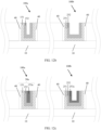
- the gate dielectric layer 151 of the first Fin FET 100a and the gate dielectric layer 251 of the second Fin FET 100b may be formed at the same time; next, as shown in FIG. 12b , the work function layer 152 of the first Fin FET 100a and the work function layer 152 of the second Fin FET 100b are formed at the same time; as shown in FIG.
- the TiSiN layer 153a of the first Fin FET 100a and the TiSiN layer 253a of the second Fin FET 100b are then formed at the same time, where the TiSiN layer 153a of the first Fin FET 100a completely fills a gap, and there is a gap in the TiSiN layer 253a of the second Fin FET 100b; and as shown in FIG. 11 , a metal filling layer 253b is finally formed in the gap of the TiSiN layer 253a of the second Fin FET 100b.
- a material of the metal filling layer may include tungsten, cobalt, or ruthenium, and is not limited herein.
- the electronic device includes a circuit board and a chip.
- the chip includes any semiconductor chip according to embodiments of this application.
- the semiconductor chip is electrically connected to the circuit board.
- a problem-resolving principle of the electronic device is similar to that of the foregoing semiconductor chip. Therefore, for implementation of the electronic device, refer to the implementation of the foregoing semiconductor chip. Details are not described herein again.
Landscapes
- Electrodes Of Semiconductors (AREA)
- Insulated Gate Type Field-Effect Transistor (AREA)
Applications Claiming Priority (1)
| Application Number | Priority Date | Filing Date | Title |
|---|---|---|---|
| PCT/CN2021/135679 WO2023102679A1 (fr) | 2021-12-06 | 2021-12-06 | Dispositif à semi-conducteurs et son procédé de fabrication, et dispositif électronique |
Publications (2)
| Publication Number | Publication Date |
|---|---|
| EP4425568A1 true EP4425568A1 (fr) | 2024-09-04 |
| EP4425568A4 EP4425568A4 (fr) | 2025-01-08 |
Family
ID=86729405
Family Applications (1)
| Application Number | Title | Priority Date | Filing Date |
|---|---|---|---|
| EP21966607.0A Pending EP4425568A4 (fr) | 2021-12-06 | 2021-12-06 | Dispositif à semi-conducteurs et son procédé de fabrication, et dispositif électronique |
Country Status (3)
| Country | Link |
|---|---|
| EP (1) | EP4425568A4 (fr) |
| CN (1) | CN116569342A (fr) |
| WO (1) | WO2023102679A1 (fr) |
Family Cites Families (10)
| Publication number | Priority date | Publication date | Assignee | Title |
|---|---|---|---|---|
| US6911391B2 (en) * | 2002-01-26 | 2005-06-28 | Applied Materials, Inc. | Integration of titanium and titanium nitride layers |
| US20080282535A1 (en) * | 2007-05-15 | 2008-11-20 | Qimonda Ag | Method of fabricating an integrated circuit |
| US9034716B2 (en) * | 2013-01-31 | 2015-05-19 | Taiwan Semiconductor Manufacturing Company, Ltd. | Method of making a FinFET device |
| CN104425575A (zh) * | 2013-09-03 | 2015-03-18 | 联华电子股份有限公司 | 金属栅极结构及其制作方法 |
| JP6832785B2 (ja) * | 2016-08-08 | 2021-02-24 | 東京エレクトロン株式会社 | シリコン窒化膜の成膜方法および成膜装置 |
| US10468258B1 (en) * | 2018-06-12 | 2019-11-05 | Taiwan Semiconductor Manufacturing Company, Ltd. | Passivator for gate dielectric |
| US10515807B1 (en) * | 2018-06-14 | 2019-12-24 | Taiwan Semiconductor Manufacturing Co., Ltd. | Methods of fabricating semiconductor devices with metal-gate work-function tuning layers |
| US11587791B2 (en) * | 2018-10-23 | 2023-02-21 | Taiwan Semiconductor Manufacturing Company, Ltd. | Silicon intermixing layer for blocking diffusion |
| US10720431B1 (en) * | 2019-01-25 | 2020-07-21 | Taiwan Semiconductor Manufacturing Co., Ltd. | Methods of fabricating semiconductor devices having gate-all-around structure with oxygen blocking layers |
| KR102942049B1 (ko) * | 2021-06-11 | 2026-03-23 | 에스케이하이닉스 주식회사 | 반도체 장치 및 그 제조 방법 |
-
2021
- 2021-12-06 CN CN202180037295.8A patent/CN116569342A/zh active Pending
- 2021-12-06 WO PCT/CN2021/135679 patent/WO2023102679A1/fr not_active Ceased
- 2021-12-06 EP EP21966607.0A patent/EP4425568A4/fr active Pending
Also Published As
| Publication number | Publication date |
|---|---|
| EP4425568A4 (fr) | 2025-01-08 |
| WO2023102679A1 (fr) | 2023-06-15 |
| CN116569342A (zh) | 2023-08-08 |
Similar Documents
| Publication | Publication Date | Title |
|---|---|---|
| US11784260B2 (en) | Semiconductor devices | |
| US12581634B2 (en) | Semiconductor devices incorporating semiconductor layer configurations and methods of manufacturing the same | |
| US12224210B2 (en) | Method for FinFet fabrication and structure thereof | |
| US20250098222A1 (en) | Field effect transistor with disabled channels and method | |
| US11011625B2 (en) | Liner for a bi-layer gate helmet and the fabrication thereof | |
| US11309417B2 (en) | Method of manufacturing a semiconductor device and a semiconductor device | |
| US20260082894A1 (en) | Field effect transistor with source/drain via and method | |
| US20230178600A1 (en) | Semiconductor Device Structure and Method for Forming the Same | |
| CN114121948A (zh) | 半导体装置 | |
| US20210167193A1 (en) | Method and Device for Forming Metal Gate Electrodes for Transistors | |
| US20240339355A1 (en) | Air-Replaced Spacer for Self-Aligned Contact Scheme | |
| US20230065208A1 (en) | Field effect transistor with inner spacer liner layer and method | |
| US20250359162A1 (en) | Field effect transistor with strained channels and method | |
| US20250366008A1 (en) | Field effect transistor with gate isolation structure and method | |
| EP4425568A1 (fr) | Dispositif à semi-conducteurs et son procédé de fabrication, et dispositif électronique | |
| US20240371643A1 (en) | Semiconductor device structure with gate and method for forming the same | |
| US20250359208A1 (en) | Field effect transistor with isolated source/drains and method | |
| TW202541636A (zh) | 半導體結構及其形成方法 |
Legal Events
| Date | Code | Title | Description |
|---|---|---|---|
| STAA | Information on the status of an ep patent application or granted ep patent |
Free format text: STATUS: THE INTERNATIONAL PUBLICATION HAS BEEN MADE |
|
| PUAI | Public reference made under article 153(3) epc to a published international application that has entered the european phase |
Free format text: ORIGINAL CODE: 0009012 |
|
| STAA | Information on the status of an ep patent application or granted ep patent |
Free format text: STATUS: REQUEST FOR EXAMINATION WAS MADE |
|
| 17P | Request for examination filed |
Effective date: 20240527 |
|
| AK | Designated contracting states |
Kind code of ref document: A1 Designated state(s): AL AT BE BG CH CY CZ DE DK EE ES FI FR GB GR HR HU IE IS IT LI LT LU LV MC MK MT NL NO PL PT RO RS SE SI SK SM TR |
|
| A4 | Supplementary search report drawn up and despatched |
Effective date: 20241205 |
|
| RIC1 | Information provided on ipc code assigned before grant |
Ipc: H01L 29/49 20060101ALI20241129BHEP Ipc: H01L 21/28 20060101ALI20241129BHEP Ipc: H01L 29/78 20060101ALI20241129BHEP Ipc: H01L 29/66 20060101AFI20241129BHEP |
|
| DAV | Request for validation of the european patent (deleted) | ||
| DAX | Request for extension of the european patent (deleted) |