EP4429092A1 - Convertisseur de puissance modulaire et ups - Google Patents
Convertisseur de puissance modulaire et ups Download PDFInfo
- Publication number
- EP4429092A1 EP4429092A1 EP23160632.8A EP23160632A EP4429092A1 EP 4429092 A1 EP4429092 A1 EP 4429092A1 EP 23160632 A EP23160632 A EP 23160632A EP 4429092 A1 EP4429092 A1 EP 4429092A1
- Authority
- EP
- European Patent Office
- Prior art keywords
- circuit
- switch
- converter
- diode
- sub
- Prior art date
- Legal status (The legal status is an assumption and is not a legal conclusion. Google has not performed a legal analysis and makes no representation as to the accuracy of the status listed.)
- Pending
Links
- 230000002457 bidirectional effect Effects 0.000 claims abstract description 28
- 238000000034 method Methods 0.000 claims description 36
- 229910002601 GaN Inorganic materials 0.000 claims description 4
- HBMJWWWQQXIZIP-UHFFFAOYSA-N silicon carbide Chemical compound [Si+]#[C-] HBMJWWWQQXIZIP-UHFFFAOYSA-N 0.000 claims description 4
- 229910010271 silicon carbide Inorganic materials 0.000 claims description 4
- JMASRVWKEDWRBT-UHFFFAOYSA-N Gallium nitride Chemical compound [Ga]#N JMASRVWKEDWRBT-UHFFFAOYSA-N 0.000 claims description 2
- 238000004590 computer program Methods 0.000 claims description 2
- 229910003465 moissanite Inorganic materials 0.000 claims description 2
- 239000004065 semiconductor Substances 0.000 claims description 2
- 239000003990 capacitor Substances 0.000 description 21
- 238000006243 chemical reaction Methods 0.000 description 19
- 238000010586 diagram Methods 0.000 description 7
- 230000010355 oscillation Effects 0.000 description 5
- 230000002441 reversible effect Effects 0.000 description 4
- 230000003247 decreasing effect Effects 0.000 description 2
- 238000013021 overheating Methods 0.000 description 2
- 230000002123 temporal effect Effects 0.000 description 2
- 230000007704 transition Effects 0.000 description 2
- 238000013459 approach Methods 0.000 description 1
- 230000000903 blocking effect Effects 0.000 description 1
- 238000005352 clarification Methods 0.000 description 1
- 230000001419 dependent effect Effects 0.000 description 1
- 238000013461 design Methods 0.000 description 1
- 238000007599 discharging Methods 0.000 description 1
- 238000009499 grossing Methods 0.000 description 1
- 238000009434 installation Methods 0.000 description 1
- 238000012986 modification Methods 0.000 description 1
- 230000004048 modification Effects 0.000 description 1
Images


Classifications
-
- H—ELECTRICITY
- H02—GENERATION; CONVERSION OR DISTRIBUTION OF ELECTRIC POWER
- H02M—APPARATUS FOR CONVERSION BETWEEN AC AND AC, BETWEEN AC AND DC, OR BETWEEN DC AND DC, AND FOR USE WITH MAINS OR SIMILAR POWER SUPPLY SYSTEMS; CONVERSION OF DC OR AC INPUT POWER INTO SURGE OUTPUT POWER; CONTROL OR REGULATION THEREOF
- H02M3/00—Conversion of DC power input into DC power output
- H02M3/02—Conversion of DC power input into DC power output without intermediate conversion into AC
- H02M3/04—Conversion of DC power input into DC power output without intermediate conversion into AC by static converters
- H02M3/10—Conversion of DC power input into DC power output without intermediate conversion into AC by static converters using discharge tubes with control electrode or semiconductor devices with control electrode
- H02M3/145—Conversion of DC power input into DC power output without intermediate conversion into AC by static converters using discharge tubes with control electrode or semiconductor devices with control electrode using devices of a triode or transistor type requiring continuous application of a control signal
- H02M3/155—Conversion of DC power input into DC power output without intermediate conversion into AC by static converters using discharge tubes with control electrode or semiconductor devices with control electrode using devices of a triode or transistor type requiring continuous application of a control signal using semiconductor devices only
- H02M3/156—Conversion of DC power input into DC power output without intermediate conversion into AC by static converters using discharge tubes with control electrode or semiconductor devices with control electrode using devices of a triode or transistor type requiring continuous application of a control signal using semiconductor devices only with automatic control of output voltage or current, e.g. switching regulators
- H02M3/158—Conversion of DC power input into DC power output without intermediate conversion into AC by static converters using discharge tubes with control electrode or semiconductor devices with control electrode using devices of a triode or transistor type requiring continuous application of a control signal using semiconductor devices only with automatic control of output voltage or current, e.g. switching regulators including plural semiconductor devices as final control devices for a single load
-
- H—ELECTRICITY
- H02—GENERATION; CONVERSION OR DISTRIBUTION OF ELECTRIC POWER
- H02M—APPARATUS FOR CONVERSION BETWEEN AC AND AC, BETWEEN AC AND DC, OR BETWEEN DC AND DC, AND FOR USE WITH MAINS OR SIMILAR POWER SUPPLY SYSTEMS; CONVERSION OF DC OR AC INPUT POWER INTO SURGE OUTPUT POWER; CONTROL OR REGULATION THEREOF
- H02M1/00—Details of apparatus for conversion
- H02M1/0048—Circuits or arrangements for reducing losses
- H02M1/0054—Transistor switching losses
- H02M1/0058—Transistor switching losses by employing soft switching techniques, i.e. commutation of transistors when applied voltage is zero or when current flow is zero
-
- H—ELECTRICITY
- H02—GENERATION; CONVERSION OR DISTRIBUTION OF ELECTRIC POWER
- H02M—APPARATUS FOR CONVERSION BETWEEN AC AND AC, BETWEEN AC AND DC, OR BETWEEN DC AND DC, AND FOR USE WITH MAINS OR SIMILAR POWER SUPPLY SYSTEMS; CONVERSION OF DC OR AC INPUT POWER INTO SURGE OUTPUT POWER; CONTROL OR REGULATION THEREOF
- H02M1/00—Details of apparatus for conversion
- H02M1/10—Arrangements incorporating converting means for enabling loads to be operated at will from different kinds of power supplies, e.g. from AC or DC
-
- H—ELECTRICITY
- H02—GENERATION; CONVERSION OR DISTRIBUTION OF ELECTRIC POWER
- H02M—APPARATUS FOR CONVERSION BETWEEN AC AND AC, BETWEEN AC AND DC, OR BETWEEN DC AND DC, AND FOR USE WITH MAINS OR SIMILAR POWER SUPPLY SYSTEMS; CONVERSION OF DC OR AC INPUT POWER INTO SURGE OUTPUT POWER; CONTROL OR REGULATION THEREOF
- H02M3/00—Conversion of DC power input into DC power output
- H02M3/01—Resonant DC/DC converters
-
- H—ELECTRICITY
- H02—GENERATION; CONVERSION OR DISTRIBUTION OF ELECTRIC POWER
- H02M—APPARATUS FOR CONVERSION BETWEEN AC AND AC, BETWEEN AC AND DC, OR BETWEEN DC AND DC, AND FOR USE WITH MAINS OR SIMILAR POWER SUPPLY SYSTEMS; CONVERSION OF DC OR AC INPUT POWER INTO SURGE OUTPUT POWER; CONTROL OR REGULATION THEREOF
- H02M1/00—Details of apparatus for conversion
- H02M1/0095—Hybrid converter topologies, e.g. NPC mixed with flying capacitor, thyristor converter mixed with MMC or charge pump mixed with buck
-
- H—ELECTRICITY
- H02—GENERATION; CONVERSION OR DISTRIBUTION OF ELECTRIC POWER
- H02M—APPARATUS FOR CONVERSION BETWEEN AC AND AC, BETWEEN AC AND DC, OR BETWEEN DC AND DC, AND FOR USE WITH MAINS OR SIMILAR POWER SUPPLY SYSTEMS; CONVERSION OF DC OR AC INPUT POWER INTO SURGE OUTPUT POWER; CONTROL OR REGULATION THEREOF
- H02M3/00—Conversion of DC power input into DC power output
- H02M3/02—Conversion of DC power input into DC power output without intermediate conversion into AC
- H02M3/04—Conversion of DC power input into DC power output without intermediate conversion into AC by static converters
- H02M3/06—Conversion of DC power input into DC power output without intermediate conversion into AC by static converters using resistors or capacitors, e.g. potential divider
- H02M3/07—Conversion of DC power input into DC power output without intermediate conversion into AC by static converters using resistors or capacitors, e.g. potential divider using capacitors charged and discharged alternately by semiconductor devices with control electrode, e.g. charge pumps
Definitions
- the invention relates to the field of power converters, particularly to an unidirectional or bidirectional DC/DC, DC/AC, AC/DC or DC/AC converter, and to an uninterruptible power supply, UPS.
- the invention further relates to a method, to a program element, and to a computer-readable storage medium.
- UPS Uninterruptible Power Supply
- UPS Uninterruptible Power Supply
- DC-Link a central node of a UPS system
- the solution strategy is based on a highly modular concept of the subsystems. Due to this modular concept, the basic principle, the subsystems and/or the components may not only be used for (or applied to) a UPS, but also for DC/DC converters. As explained in detail further below, this principle may also be applied to to a DC/AC converter, to an AC/DC converter, and to an AC/AC converter, in a unidirectional and/or bidirectional version, and to a UPS, which may be connected to an AC and/or to a DC input and to an AC output or to a DC output.
- the principle will firstly be explained based on an embodiment with a lowest number of components, and modular extensions will be introduced in a stepwise way.
- One aspect relates to a unidirectional DC/AC converter, comprising:
- a DC/DC converter converts a DC input voltage ("DC source”) to an DC output voltage, which is usually connected to a load, i.e. any consumer of DC power.
- a unidirectional DC/DC converter has a DC source connected to its input side and a load connected to its output side.
- a bidirectional DC/DC converter has a DC source connected to its input side and a load connected to its output side, and the "output side” can, additionally, be used as power source and the "input side” can, additionally, be used as power sink, usually for loading an accumulator (or similar devices, e.g. a capacitor) on the "input side”.
- This input sub-circuit is arranged between a DC source and a central node.
- the "central node” may have a similar position as a so-called “DC-Link" of a traditional UPS system.
- the DC/DC converter comprises a DC input sub-circuit comprising a forwarded first diode and a first switch arranged in series.
- a "forwarded" diode is a diode arranged in forward direction or pass direction
- a “backwarded” diode is a diode arranged in reverse direction or blocking direction. For instance, if the DC source has its plus terminal connected to an input terminal of the DC/DC converter, the diode's anode side is oriented towards the input terminal.
- the first switch is arranged in series with said forwarded first diode.
- the DC/DC converter further comprises an output sub-circuit comprising a forwarded second diode and a second switch arranged in series.
- the output sub-circuit is arranged between the central node and a DC load.
- a capacitor may be arranged in parallel to the DC load, e.g. for further reducing the output's ripple.
- the DC/DC converter further comprises a central sub-circuit.
- the central sub-circuit comprises an inductance, which is arranged in series with and directly connected to a parallel arrangement of: (i) a first capacitance, (ii) a forwarded third diode and a third switch arranged in series, and (iii) a backwarded fourth diode.
- the backwarded fourth diode may be used for discharging the inductance completely; see below for further details.
- the inductance and the first capacitance of the central sub-circuit may build a series resonant circuit, whose resonance frequency may be quite high, e.g. higher than 10 kHz, 50 kHz, or even higher than 200 kHz.
- the resonance frequency may depend on the switches that are used in the DC/DC converter.
- the central sub-circuit has, additionally, the third switch arranged in series with a forwarded third diode. This switch (arranged in series with a forwarded third diode) is arranged in parallel to the capacitance, so that - in an early phase of the conversion - current can flow through the inductance without needing to pass through the first capacitance.
- the capacitance gets more energy than if the swinging would had started without a pre-charged inductance.
- the resulting energy in the inductance may depend on the duration of having the third switch closed.
- the power and/or the voltage delivered to the output load may be controlled by the closing time of the third switch (and additional factors, like the "pausing time” between conversion cycles; see below).
- This principle does not only lead to significantly lower dimensions of the converter, e.g. due to the high frequency at which the converter is operated. As a result, the components and/or subsystems of the converter may be improved, e.g. in terms of size and/or cost. Furthermore, this principle can be used both for a boost converter and for a buck converter.
- a boost converter U out > U in
- the duration of having the third switch closed may be varied, depending on the desired output voltage U out .
- the third switch may be kept open, and only the switching frequency of the first switch (controlled indirectly by the duration of "pauses") may be varied, depending on the desired output voltage U out .
- the forwarded third diode and the third switch may be abandoned.
- the voltage regulation may only have an impact on the duration of the "pauses".
- the pulse width of the first switch is determined by the inductor and the capacitance and, thus, cannot vary.
- an additional DC input sub-circuit is added, which is configured to be connected to a second DC source that has an opposite polarity than the (first) DC source. For instance, if the DC input sub-circuit is connected to a plus terminal of the (first) DC source, the additional DC input sub-circuit is connected to a minus terminal of the second DC source. Due to this, the load cannot only by supplied with a positive half-wave, but also with a negative half-wave, so that an AC-wave can be built at the converter's output.
- An aspect relates to a unidirectional AC/AC converter or AC/DC converter, comprising:
- the bidirectional DC/DC converter may be used, for instance, to load a Battery (e.g. an accumulator or similar devices, e.g. a capacitor) on the "input side" of the converter.
- a Battery e.g. an accumulator or similar devices, e.g. a capacitor
- the input sub-circuit gets - additionally to the input sub-circuit of the unidirectional DC/DC converter as described above - an antiparallel input sub-circuit, the antiparallel input sub-circuit being arranged in parallel to the input sub-circuit, wherein the diode of the antiparallel input sub-circuit (i.e. the "backwarded first diode”) is arranged in a direction reverse to the forwarded first diode.
- the output sub-circuit gets an antiparallel output sub-circuit, whose diode (i.e. the "backwarded second diode”) is arranged in a direction reverse to the forwarded second diode.
- the central sub-circuit of the bidirectional converter is slightly modified:
- the branch with the fourth diode gets a (fourth) switch arranged in series with the backwarded fourth diode.
- This modification makes it also possible to reverse the polarity of the power source at the input terminal (e.g. the DC source's minus connected to the input terminal, instead of plus) and/or at the output terminal.
- An aspect relates to an uninterruptible power supply, UPS, comprising:
- the UPS has an additional AC branch, comprising the AC input sub-circuit and the antiparallel AC input sub-circuit.
- the AC source is checked for its current voltage. When the AC source's current voltage is high enough, power is taken from the AC source. When the AC source's current voltage is not high enough, power is taken from the DC source. When the AC source's current voltage is high enough and the DC source (e.g. an accumulator) needs power, power is taken from the AC source and the DC source may be charged.
- the DC source e.g. an accumulator
- the hardware of the AC branch looks the same as the hardware of the DC branch (comprising a DC input sub-circuit and an antiparallel input sub-circuit); only the control of AC branch's switches need to be changed. This allows advantageously a very modular design of the UPS and/or the converters.
- the UPS or the bidirectional DC/DC converter further comprises an additional DC input sub-circuit and an additional antiparallel input sub-circuit that are arranged between a second DC source and the central node, wherein a second terminal of the DC source and a second terminal of the second DC source are connected to ground.
- the DC/DC converter may be considered as a UPS without AC branch. This arrangement advantageously allows to deliver also a negative half-wave to the central node and, consequently, to the central sub-circuit. This may allow to provide a positive DC at the UPS' output terminal, a negative DC, and/or to provide an AC output.
- the bidirectional DC/DC converter (and the respective part of the UPS) can also be operated as a DC/AC converter, as a AC/DC converter, and/or as a AC/AC converter.
- the four quarters (Q1 - Q4) of a sine may be operated like this: In Q1, the energy of the inductance is stepwise - i.e. in a sine-form - increased, in positive direction; in Q2 the energy of the inductance is stepwise (in a sine-form) decreased; in Q3, the energy of the inductance is stepwise (in a sine-form) increased, in negative direction; in Q4 the energy of the inductance is stepwise (in a sine-form) decreased.
- the UPS further comprises one or more additional AC input sub-circuits and antiparallel AC input sub-circuits. This is particularly advantageous for, e.g., supporting a UPS that is connected to a three-phase high-power source.
- the mid of a three-phase Y or Delta arrangement may be connected to the ground between the DC sources and/or to the ground of the load.
- the UPS further comprises one or more additional DC input sub-circuits and antiparallel input sub-circuits. This is particularly advantageous for, e.g., supporting a plurality of solar panels and/or other sources of renewable energy.
- the UPS further comprises one or more additional output sub-circuits and antiparallel output sub-circuits. This is particularly advantageous for, e.g., a UPS for a plurality of DC loads.
- the switches of the unidirectional DC/AC converter, of the bidirectional DC/AC converter, and/or of the UPS are implemented as a MOSFET, an IGBT, a thyristor, a silicon carbide, SiC, and/or a gallium nitride, GaN, semiconductor.
- the various types of converters and/or the UPS are designed for a DC voltage source with a voltage between 100 V and 1500 V, particularly between 200 V and 800 V.
- the voltage range of the converter may vary from a few Volts (say: 5 V) to more than 3000 V, which corresponds to double the voltage of, e.g., commercially available IGBTs.
- the DC/DC converter can be used for a broad range of DC - and, if applicable, AC - voltage sources, both for small and middle-range devices, but also for high-power converters, including, e.g., converters for charging electric vehicles, servers and/or server farms, for an intermediate device (i.e. between generating, storing and consumer units) for renewable energy.
- the switches of the unidirectional DC/AC converter, of the bidirectional DC/AC converter, and/or of the UPS are implemented as a MOSFET with a body diode, and the body diode substitutes the diode of the antiparallel sub-circuit.
- the body diode is sometimes called the "inverted diode" of the MOSFET.
- the switches of the input sub-circuit, the output sub-circuit, and/or the central sub-circuit are arranged in series, with the corresponding body diodes each arranged in opposite direction.
- the control may use the body diodes only in the last phase of unloading the inductance. This may advantageously minimize the energy through the body diodes, thus preventing them from overheating.
- the central sub-circuit is operated at a frequency between 10 kHz and 200 kHz, particularly between 20 kHz and 100 kHz, particularly between 40 kHz and 70 kHz, at about 50 kHz.
- a first capacitance of less than or about 5 ⁇ F may be used, and an inductance of less than or about 5 ⁇ H.
- the first capacitance may be significantly smaller than the second capacitance at the output.
- a second capacitance between, e.g., 50 ⁇ F and 500 ⁇ F may be taken,
- An aspect relates to a use of a unidirectional DC/AC converter, a bidirectional DC/AC converter, and/or a UPS as described above and/or below for providing a DC power output, and/or use of a bidirectional DC/AC converter, and/or a UPS as described above and/or below for providing an AC power output, and a DC power input or an AC power input.
- An aspect relates to a method for operating a unidirectional DC/DC converter as described above and/or below in a first mode, the method comprising the steps of: opening all switches; closing the first switch; opening the first switch; closing the second switch; and opening all switches.
- One conversion cycle may last from the first "opening all switches" to the last "opening all switches".
- This mode may be a so-called buck mode, i.e. with U out ⁇ U in .
- the third switch may be kept open, and only the switching frequency of the first switch may be varied, depending on the desired output voltage U out .
- the third diode and the third switch is always open and, thus, could be abandoned.
- An aspect relates to a method for operating a unidirectional DC/DC converter as described above and/or below in a second mode, the method comprising the steps of: opening all switches; closing the first switch and the third switch; opening the third switch; opening the first switch; closing the second switch (sometimes along with the fourth switch); and opening all switches.
- One conversion cycle may last from the first "opening all switches" to the last "opening all switches".
- This mode may be a so-called boost mode, i.e. with U out > U in .
- An aspect relates to a method for operating a UPS as described above and/or below, the method comprising the steps of: opening all switches; closing the fifth switch and the third switch (for getting power from the AC branch); opening the third switch; opening the fifth switch; closing the second switch (sometimes along with the fourth switch); and opening all switches.
- the methods described above for operating a unidirectional DC/DC converter and for operating a UPS are used in a mutually exclusive way. For instance, as long as the AC source(s) work(s) fine, power from the AC branch is used; when the power from the AC source (via the AC branch) is not sufficient, power from the DC source(s) is used. This may be decided, e.g. by a control device, right before each conversion cycle.
- the duration of step "opening all switches” is between 0.5 us and 1000 ⁇ s (or may be even longer if the load is very low), particularly between 1 ⁇ s and 200 ⁇ s.
- the duration may depend on the frequency the central sub-circuit is operated with.
- This step may also be called “pausing step” or "pause". The duration of the pause may influence the output's power and/or voltage.
- An aspect relates to a non-transitory computer-readable storage medium comprising computer program instructions stored therein, which, when executed on a control device that is configured for controlling controllable switches of a unidirectional DC/AC, of a bidirectional DC/AC converter, and/or of a UPS as described above and/or below, instructs the control device to perform the method described above and/or below.
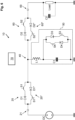
- Fig. 1 shows schematically a unidirectional DC/DC converter 10 according to an embodiment.
- the DC/DC converter 10 is connected to a DC source "DC", via an input terminal 21.
- the DC/DC converter 10 comprises a DC input sub-circuit 20.
- the input sub-circuit 20 is arranged between the DC source "DC” and a central node 40.
- the DC input sub-circuit 20 comprises a forwarded first diode D1 and a first switch S1 arranged in series.
- the DC input is connected to a plus terminal of the DC source. In this case, the diode's anode side is oriented towards the input terminal.
- the DC/DC converter 10 further comprises an output sub-circuit 60 comprising a forwarded second diode D2 and a second switch S2 arranged in series.
- the output sub-circuit 60 is arranged between the central node 40 and a load "Load", which is connected to an output terminal 69.
- the input voltage between the input terminal 21 and ground is called “U in ", and the output voltage between output terminal 69 and ground is called “U out ".
- a second capacitance C2 may be arranged, particularly for further reducing the output's ripple.
- the DC/DC converter 10 comprises a central sub-circuit 51.
- This central sub-circuit 51 comprises an inductance L1 in series with and directly connected to a parallel arrangement of: (i) a first capacitance C1, (ii) a forwarded third diode D3 and a third switch S3 arranged in series, and (iii) a backwarded fourth diode D4.
- the central sub-circuit 51 may be operated at frequencies above 10 kHz, e.g. at a frequency of 50 kHz.
- the first capacitance C1 may have a capacity of less than or about 5 ⁇ F, and the inductance L1 may have a value of less than or about 5 ⁇ H.
- the first capacitance C1 may be significantly smaller than the second capacitance C2 at the output.
- a second capacitance between, e.g., 50 ⁇ F and 500 ⁇ F may be taken.
- the switches S1 - S3 may be controlled by a control device 70.
- the control device 70 may be operated according to a method, e.g., shown in Fig. 2 and/or Fig. 3 .
- Fig. 2 shows schematically a method of operating the DC/DC converter 10 of Fig. 1 as a buck converter (U out ⁇ U in ) according to an embodiment.
- all switches S1 - S3 are open or opened.
- the first switch S1 is closed, thus increasing current through inductance L1 (up to turning point) and voltage at capacitor (or capacitance) C1, up to a peak voltage of about 2 ⁇ U in , because of the resonance of the series-L1-C1-circuit.
- the first switch S1 is opened.
- the second switch S2 towards the output, is closed.
- the fourth (not-controlled) diode D4 empties the energy in inductance L1.
- the fourth diode D4 is a crucial component for finishing each conversion cycle correctly, i.e. to discharge the inductance L1without leaving energy in said inductance L1. Otherwise, the voltage of capacitor C1 would become negative and in the next step it would be impossible to "start from zero" for each conversion cycle, i.e. to start each conversion cycle from a condition where the series-L1-C1-circuit is completely "reset", i.e. the components of the series-L1-C1-circuit have zero current and voltage (possibly only having a very small - i.e. a very negligible - residual energy).
- Fig. 3 shows schematically a method of operating the DC/DC converter 10 of Fig. 1 as a boost converter (U out > U in ) or for U out ⁇ U in , according to an embodiment.
- all switches S1 - S3 are open or opened.
- the first switch S1 and the third switch S3 is closed, thus shorting capacitor C1 and pre-charging inductance L1, before starting the oscillation of the series-L1-C1-circuit.
- the duration of the first step determines the current and/or energy that is injected to the inductance L1.
- the third switch S3 is opened, thus increasing current through inductance L1 (up to turning point) and voltage at capacitor C1, up to a peak.
- the first switch S1 is opened.
- the second switch S2 towards the output, is closed.
- the fourth (not-controlled) diode D4 empties the energy in inductance L1.
- all switches S1 - S3 are opened, thus finishing this conversion cycle.
- Fig. 4 shows schematically a DC/AC converter 10 according to an embodiment.
- the DC/AC converter 10 comprises, compared to the DC/DC converter of Fig. 1 , an additional DC input sub-circuit 25 comprising a forwarded sixth diode D6 and a sixth switch S6 arranged in series, arranged between a second DC source DC2 and the central node 40.
- a second terminal of the (first) DC source DC and a second terminal of the second DC source DC2 are connected to ground, This brings an (additional) negative half-wave to the a central sub-circuit 50, so that an AC-wave can be built, and the load can be supplied with an AC output.
- a capacitor C2, arranged parallel to the load, may have a smaller capacity than for an DC output.
- Fig. 5 shows schematically a AC/AC or AC/DC converter 10 according to an embodiment.
- the AC/AC or AC/DC converter 10 comprises, compared to the DC/AC converter of Fig. 4 , an AC input sub-circuit 30, instead of DC input sub-circuit 20 and the additional DC input sub-circuit 25 of Fig. 4 .
- the AC input sub-circuit 30 comprises a forwarded fifth diode D5 and a fifth switch S5 arranged in series, and an antiparallel AC input sub-circuit 30* comprising a backwarded fifth diode D5* and an antiparallel fifth switch S5* arranged in series.
- the AC input sub-circuit 30 and the antiparallel AC input sub-circuit 30* are arranged between a AC source AC and the central node 40.
- the output power provided at the output terminal 69 can be either DC or AC.
- a capacitor C2, arranged parallel to the load, may have a smaller capacity for AC output than for DC output.
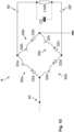
- Fig. 6 shows schematically a bidirectional DC/DC converter 10 according to an embodiment.
- the DC/DC converter 10 comprises a DC input sub-circuit 20 comprising a forwarded first diode D1 and a first switch S1 arranged in series, and an antiparallel input sub-circuit 20* comprising a backwarded first diode D1* and an antiparallel first switch S1* arranged in series, the input sub-circuit 20 and the antiparallel input sub-circuit 20* being arranged between a DC source DC and a central node 40.
- the DC/DC converter 10 further comprises an output sub-circuit 60 comprising a forwarded second diode D2 and a second switch S2 arranged in series, and an antiparallel output sub-circuit 60* comprising a backwarded second diode D2* and an antiparallel second switch S2* arranged in series, the output sub-circuit 60 and the antiparallel output sub-circuit 60* being arranged between the central node 40 and a load Load.
- the DC/DC converter 10 comprises a central sub-circuit 50 comprising an inductance L1 in series with and directly connected to a parallel arrangement of: (i) a first capacitance C1, (ii) a forwarded third diode (D3) and a third switch S3 arranged in series, and (iii) a backwarded fourth diode D4 and a fourth switch S4 arranged in series.
- the DC/DC converter 10 of Fig. 6 is bidirectional, because output terminal 69 can not only be used for connecting to a load, but also connecting to a power source for providing power.
- the power is, then led via the antiparallel output sub-circuit 60* to the central node 40 and, further, led to input terminal 21.
- the input terminal 21 may be connected to an accumulator.
- the accumulator may act as a DC source as long as power needs to be delivered to output terminal 69. When power is delivered from the output terminal 69, the accumulator may be charged. This may, e.g., be used for sources of renewable energy, whose power may vary during the day, and/or for many other purposes, e.g.
- the switches S1 - S4, S1* and S2* of Fig. 6 may be controlled by a control device 70.
- the control device 70 may be operated according to a method, e.g., shown in Fig. 2 and/or Fig. 3 .
- Fig. 7 shows schematically a UPS 11 according to an embodiment. It is clearly visible that UPS 11 differs from the DC/DC converter 10 of Fig. 6 by an additional AC branch comprising an AC input sub-circuit 30 and an antiparallel AC input sub-circuit 30*.
- the AC input sub-circuit 30 comprises a forwarded fifth diode D5 and a fifth switch S5 arranged in series.
- the antiparallel AC input sub-circuit 30* comprises a backwarded fifth diode D5* and an antiparallel fifth switch S5* arranged in series.
- the AC branch is arranged between a AC source "AC" and the central node 40.
- the AC source may be checked for its current voltage.
- the AC source's current voltage is high enough, power is taken from the AC source.
- the AC source's current voltage is not high enough, power is taken from the DC source.
- the DC source e.g. an accumulator
- the switches S1 - S5, S1*, S2* and S5* of Fig. 7 may be controlled by a control device 70.
- the control device 70 may be operated according to a method, e.g., shown in Fig. 2 , Fig. 3 and/or Fig. 11 .
- Fig. 8 shows schematically a UPS 11 according to an embodiment.
- the UPS 11 Fig. 6 has an additional DC input sub-circuit 25, arranged between a second DC source DC2 and the central node 40.
- the DC input sub-circuit 25 comprises a forwarded sixth diode D6 and a sixth switch S6 arranged in series.
- the antiparallel DC input sub-circuit 25* comprises a backwarded sixth diode D6* and an antiparallel sixth switch S6* arranged in series.
- a second (minus) terminal of the DC source "DC” and a second (plus) terminal of the second DC source "DC2" are connected to ground.
- the switches S1 - S6, S1*, S2*, S5* and S6* of Fig. 6 may be controlled by a control device 70.
- the control device 70 may be operated according to a method, e.g., shown in Fig. 2 , Fig. 3 and/or Fig. 11 . Note that these figures only show the current through inductance L1 and the voltage at capacitor C1 for a positive half-wave. It is clear that for a negative half-wave the current through inductance L1 and the voltage at capacitor C1 have opposite directions.
- this additional DC input sub-circuit 25 can also be applied to the DC/DC converter 10 of Fig. 6 , thus enabling said DC/DC converter 10 to build, additionally, a negative half-wave. This may also be used to build a DC/AC converter and/or to build a UPS with AC output.
- the UPS 11 of Fig. 8 or Fig. 7 may contain not only one AC branch, but a plurality of AC branches.
- the UPS may be able to be connected to a 3-phase AC source, e.g. in Y or Delta configuration.
- Fig. 9 shows another embodiment of the UPS of Fig. 8 according to an embodiment.
- a part of the UPS is shown, namely the part from the central node 40.
- the other parts of the circuit may be identical to the ones depicted in Fig. 8 .
- one load is connected between the output sub-circuit 60 and ground, and another load is connected between the antiparallel output sub-circuit 60* and ground. Note that this circuit part may also be applied, e.g., to the circuit of Fig. 7 .
- Fig. 10 shows another embodiment of the UPS of Fig. 7 or 8 and/or of the converter of any of Figs. 1 , 4 , 5 , or 6 according to an embodiment.
- a bridge B is depicted as a bridge of four branches, each branch of the bridge comprising a diode D_a, D_b, D_c, D_d and a switch S_a, S_b, S_c, S_d arranged in series.
- the underscore “_" is substituted by a "2", for an analogous naming of the output sub-circuit 60.
- each branch 60a, 60b, 60c, 60d of the bridge B gets an antiparallel output sub-circuit branch 60a*, 60b*, 60c*, 60d* added (not shown in Fig. 10 ).
- the DC input sub-circuit 20 (and, if applicable, also the antiparallel DC input sub-circuit 20*) may be substituted by a "DC input bridge", which looks similar to the bridge B, which is shown in Fig. 10 for the output part.
- the AC input sub-circuit 30 (and, if applicable, also the antiparallel AC input sub-circuit 30*) may be substituted by an "AC input bridge", which looks similar to the bridge B.
- Fig. 11 shows schematically a method according to an embodiment.
- This method is able to use power from an AC source e.g. ("mains") and may work as a boost converter (U out > U in ) or for U out ⁇ U in , according to an embodiment.
- mains AC source
- boost converter U out > U in
- U out ⁇ U in boost converter
- all switches S1 - S5, S1*, S2* and S5* (of Fig. 7 , plus S6 and S6* of Fig. 6 ) are open or opened.
- the fifth switch S5 and the third switch S3 are closed, thus shorting capacitor C1 and pre-charging the inductance L1, before starting the oscillation of the series-L1-C1-circuit.
- the duration of the first step determines the current and/or energy that is injected to the inductance L1.
- the third switch S3 is opened, thus increasing current through inductance L1 (up to turning point) and voltage at capacitor C1, up to a peak.
- the fifth switch S5 is opened.
- the second switch S2 towards the output, and the fourth switch S4 are closed.
- the fourth diode D4 empties, via S4, the energy in inductance L1.
- all switches S1 - S4 are opened, thus finishing this conversion cycle.
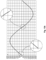
- the filled circles in the diagram of current through inductance L1 mark a zero current transition, the hollow circles mark a zero voltage transition.
- Fig. 12 schematically shows a partial circuit according to an embodiment.
- This partial circuit is a variation of building a sub-circuit and its antiparallel input sub-circuit, e.g. the DC input sub-circuit 20 and the antiparallel input sub-circuit 20* of any of figures Fig. 6 to Fig. 6 .
- the partial circuit comprises two MOSFETs, i.e. MOSFET #1 and MOSFET #2.
- the body diode of MOSFET #2 serves as forwarded diode Dx of the sub-circuit comprising switch Sx and Dx
- the body diode of MOSFET #1 serves as backwarded diode Dx* of the antiparallel sub-circuit comprising switch Sx* and Dx*.
- the control may use the body diodes only in the last phase of unloading the inductance.
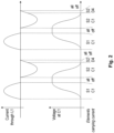
- Fig. 13a and 13b show signals of a UPS or of an AC/AC converter according to an embodiment.
- Fig. 13a shows an AC input signal with significant ripples, i.e. deviations for a pure sine curve.
- Fig. 13b shows an AC output signal, i.e. after having applied one of the methods described above and/or below, but with a small smoothing capacitor. It is clearly visible that this signal approaches a pure sine curve in a significantly better way than the AC input signal, in spite of the bad quality of this input signal. Furthermore, it is clearly visible that this "close-to-sine curve" is built of waves of essentially higher frequency.
- the "close-to-sine curve” may have a frequency of 50 Hz or 60 Hz, whereas the partial curves the "close-to-sine curve” is built of has a frequency higher (or much higher) than, e.g., 10 kHz.
- “pauses” are clearly visible, nearby the value zero of this "close-to-sine curve”.
- Fig. 14 shows a flow diagram 100 according to an embodiment. This method may be used for operating the DC/DC converter 10 of Fig. 1 as a buck converter (U out ⁇ U in ).
- a starting step 102 all switches S1 - S3 are open.
- the first switch S1 is closed, thus increasing current through inductance L1 and voltage at capacitor C1.
- the first switch S1 is opened.
- the second switch S2 towards the output, is closed.
- the fourth (not-controlled) diode D4 empties the energy in inductance L1.
- all switches S1 - S3 are opened, thus finishing this conversion cycle.
- the temporal distance ("pause") to the next conversion cycle, starting with the step 104 influences the voltage and/or energy to be transferred to the output.
- Fig. 15 shows a flow diagram 200 according to an embodiment. This method may be used for operating the DC/DC converter 10 of Fig. 1 as a boost converter (U out > U in ) or for U out ⁇ U in .
- a starting step 202 all switches S1 - S3 are open or opened.
- the first switch S1 and the third switch S3 are closed, thus shorting capacitor C1 and pre-charging inductance L1, before starting the oscillation of the series-L1-C1-circuit.
- the duration of the step 204 determines the current and/or energy that is injected to the inductance L1.
- the third switch S3 is opened, thus increasing current through inductance L1 and voltage at capacitor C1.
- a step 208 the first switch S1 is opened.
- the second switch S2, towards the output, and the fourth switch S4 are closed.
- the fourth (not-controlled) diode D4 empties the energy in inductance L1.
- all switches S1 - S4 are opened, thus finishing this conversion cycle.
- Fig. 16 shows a flow diagram 300 according to an embodiment.
- This method is able to use power from an AC source e.g. ("mains") and may work as a boost converter (U out > U in ) or for U out ⁇ U in , according to an embodiment.
- mains AC source
- boost converter U out > U in
- U out ⁇ U in boost converter
- all switches S1 - S5, S1*, S2* and S5* (of Fig. 7 , plus S6 and S6* of Fig. 6 ) are open or opened.
- the fifth switch S5 and the third switch S3 are closed, thus shorting capacitor C1 and pre-charging the inductance L1, before starting the oscillation of the series-L1-C1-circuit.
- the duration of this step determines the current and/or energy that is injected into the inductance L1.
- the third switch S3 is opened, thus increasing current through inductance L1 and voltage at capacitor C1.
- the fifth switch is opened.
- the second switch S2 towards the output, and the fourth switch S4 are closed.
- the fourth diode D4 empties the energy in inductance L1.
- all switches S1 - S4 are opened, thus finishing this conversion cycle.
Landscapes
- Engineering & Computer Science (AREA)
- Power Engineering (AREA)
- Ac-Ac Conversion (AREA)
Priority Applications (1)
| Application Number | Priority Date | Filing Date | Title |
|---|---|---|---|
| EP23160632.8A EP4429092A1 (fr) | 2023-03-08 | 2023-03-08 | Convertisseur de puissance modulaire et ups |
Applications Claiming Priority (1)
| Application Number | Priority Date | Filing Date | Title |
|---|---|---|---|
| EP23160632.8A EP4429092A1 (fr) | 2023-03-08 | 2023-03-08 | Convertisseur de puissance modulaire et ups |
Publications (1)
| Publication Number | Publication Date |
|---|---|
| EP4429092A1 true EP4429092A1 (fr) | 2024-09-11 |
Family
ID=85510849
Family Applications (1)
| Application Number | Title | Priority Date | Filing Date |
|---|---|---|---|
| EP23160632.8A Pending EP4429092A1 (fr) | 2023-03-08 | 2023-03-08 | Convertisseur de puissance modulaire et ups |
Country Status (1)
| Country | Link |
|---|---|
| EP (1) | EP4429092A1 (fr) |
Citations (2)
| Publication number | Priority date | Publication date | Assignee | Title |
|---|---|---|---|---|
| US4720667A (en) * | 1986-06-20 | 1988-01-19 | Lee Fred C | Zero-current switching quasi-resonant converters operating in a full-wave mode |
| US9178422B2 (en) * | 2013-02-21 | 2015-11-03 | Texas Instruments Incorporated | Resonance-based single inductor output-driven DC-DC converter and method |
-
2023
- 2023-03-08 EP EP23160632.8A patent/EP4429092A1/fr active Pending
Patent Citations (2)
| Publication number | Priority date | Publication date | Assignee | Title |
|---|---|---|---|---|
| US4720667A (en) * | 1986-06-20 | 1988-01-19 | Lee Fred C | Zero-current switching quasi-resonant converters operating in a full-wave mode |
| US9178422B2 (en) * | 2013-02-21 | 2015-11-03 | Texas Instruments Incorporated | Resonance-based single inductor output-driven DC-DC converter and method |
Non-Patent Citations (5)
| Title |
|---|
| JABBARI MASOUD ET AL: "Resonant Multi-input/Multi-output/Bidirectional ZCS Step-Down DC--DC Converter With Systematic Synthesis for Point-to-Point Power Routing", IEEE TRANSACTIONS ON POWER ELECTRONICS, INSTITUTE OF ELECTRICAL AND ELECTRONICS ENGINEERS, USA, vol. 33, no. 7, 1 July 2018 (2018-07-01), pages 6024 - 6032, XP011679898, ISSN: 0885-8993, [retrieved on 20180319], DOI: 10.1109/TPEL.2017.2749326 * |
| MASOUD JABBARI: "Unified Analysis of Switched-Resonator Converters", IEEE TRANSACTIONS ON POWER ELECTRONICS, INSTITUTE OF ELECTRICAL AND ELECTRONICS ENGINEERS, USA, vol. 26, no. 5, 1 May 2011 (2011-05-01), pages 1364 - 1376, XP011357250, ISSN: 0885-8993, DOI: 10.1109/TPEL.2010.2079954 * |
| SARO L ET AL: "High-voltage MOSFET behavior in soft-switching converters: analysis and reliability improvements", TELECOMMUNICATIONS ENERGY CONFERENCE, 1998. INTELEC. TWENTIETH INTERNA TIONAL SAN FRANCISCO, CA, USA 4-8 OCT. 1998, PISCATAWAY, NJ, USA,IEEE, US, 4 October 1998 (1998-10-04), pages 30 - 40, XP010350565, ISBN: 978-0-7803-5069-4 * |
| SHAHALAMI S H ET AL: "Simulation and implementation of a new topology in Multi-Output DC-DC resonant converters based on SwRC converters", POWER ELECTRONICS, DRIVE SYSTEMS AND TECHNOLOGIES CONFERENCE (PEDSTC), 2011 2ND, IEEE, 16 February 2011 (2011-02-16), pages 75 - 80, XP031936693, ISBN: 978-1-61284-422-0, DOI: 10.1109/PEDSTC.2011.5742501 * |
| VIJYASHREE M R ET AL: "A triple output variable power switched resonant converter", 2012 INTERNATIONAL CONFERENCE ON ADVANCES IN ENGINEERING, SCIENCE AND MANAGEMENT (ICAESM 2012) : NAGAPATTINAM, TAMIL NADU, INDIA, 30 - 31 MARCH 2012, IEEE, PISCATAWAY, NJ, 30 March 2012 (2012-03-30), pages 340 - 346, XP032185499, ISBN: 978-1-4673-0213-5 * |
Similar Documents
| Publication | Publication Date | Title |
|---|---|---|
| EP2313966B1 (fr) | Système d'énergie électrique avec redresseur à modulation d'impulsions en durée (pwm) haute densité | |
| JP5059879B2 (ja) | 三相で高電力の無停電電源 | |
| KR100753462B1 (ko) | 가스 방전 처리의 전력 공급 유닛 | |
| EP2871760B1 (fr) | Précharge dépourvue de résistance | |
| US20090285005A1 (en) | Space-saving inverter with reduced switching losses and increased life | |
| CN112930645B (zh) | 开关串转换器 | |
| WO2011089483A1 (fr) | Convertisseur de courant de cc en cc | |
| US8315076B2 (en) | Circuit arrangement having a dual coil for producing an alternating voltage or an alternating current | |
| WO2015118122A1 (fr) | Alimentation électrique sans coupure comportant un convertisseur abaisseur-élévateur d'équilibrage | |
| US6940188B2 (en) | Electric power converting device | |
| KR101556933B1 (ko) | 무정전 전원장치 | |
| EP4429092A1 (fr) | Convertisseur de puissance modulaire et ups | |
| US7583066B2 (en) | Method of operating a DC/DC up/down converter | |
| WO2019092305A1 (fr) | Convertisseur de puissance, centrale électrique et procédé de commande d'une centrale électrique | |
| US20230421058A1 (en) | Method for Operating a DC/DC Converter | |
| US10742135B2 (en) | Energy recovery rectifier device | |
| CN117616680A (zh) | 一种用于两个dc链路电容器的串联连接的平衡器电路、用于控制平衡器电路的方法及转换器装置 | |
| US20240364230A1 (en) | Three-phase ac/dc converter and method for operating the same | |
| US10771002B2 (en) | Device for stabilizing direct current (DC) distribution system | |
| JP2019149866A (ja) | 電力変換装置及び電力変換システム |
Legal Events
| Date | Code | Title | Description |
|---|---|---|---|
| PUAI | Public reference made under article 153(3) epc to a published international application that has entered the european phase |
Free format text: ORIGINAL CODE: 0009012 |
|
| STAA | Information on the status of an ep patent application or granted ep patent |
Free format text: STATUS: THE APPLICATION HAS BEEN PUBLISHED |
|
| AK | Designated contracting states |
Kind code of ref document: A1 Designated state(s): AL AT BE BG CH CY CZ DE DK EE ES FI FR GB GR HR HU IE IS IT LI LT LU LV MC ME MK MT NL NO PL PT RO RS SE SI SK SM TR |
|
| STAA | Information on the status of an ep patent application or granted ep patent |
Free format text: STATUS: REQUEST FOR EXAMINATION WAS MADE |
|
| 17P | Request for examination filed |
Effective date: 20250218 |