EP4429094A1 - Stromrichtersteuergerät, stromrichter und verfahren zum betrieb eines stromrichters - Google Patents
Stromrichtersteuergerät, stromrichter und verfahren zum betrieb eines stromrichters Download PDFInfo
- Publication number
- EP4429094A1 EP4429094A1 EP23161148.4A EP23161148A EP4429094A1 EP 4429094 A1 EP4429094 A1 EP 4429094A1 EP 23161148 A EP23161148 A EP 23161148A EP 4429094 A1 EP4429094 A1 EP 4429094A1
- Authority
- EP
- European Patent Office
- Prior art keywords
- power converter
- secondary side
- power
- side controller
- signal
- Prior art date
- Legal status (The legal status is an assumption and is not a legal conclusion. Google has not performed a legal analysis and makes no representation as to the accuracy of the status listed.)
- Pending
Links
Images



Classifications
-
- H—ELECTRICITY
- H02—GENERATION; CONVERSION OR DISTRIBUTION OF ELECTRIC POWER
- H02M—APPARATUS FOR CONVERSION BETWEEN AC AND AC, BETWEEN AC AND DC, OR BETWEEN DC AND DC, AND FOR USE WITH MAINS OR SIMILAR POWER SUPPLY SYSTEMS; CONVERSION OF DC OR AC INPUT POWER INTO SURGE OUTPUT POWER; CONTROL OR REGULATION THEREOF
- H02M3/00—Conversion of DC power input into DC power output
- H02M3/22—Conversion of DC power input into DC power output with intermediate conversion into AC
- H02M3/24—Conversion of DC power input into DC power output with intermediate conversion into AC by static converters
- H02M3/28—Conversion of DC power input into DC power output with intermediate conversion into AC by static converters using discharge tubes with control electrode or semiconductor devices with control electrode to produce the intermediate AC
- H02M3/325—Conversion of DC power input into DC power output with intermediate conversion into AC by static converters using discharge tubes with control electrode or semiconductor devices with control electrode to produce the intermediate AC using devices of a triode or a transistor type requiring continuous application of a control signal
- H02M3/335—Conversion of DC power input into DC power output with intermediate conversion into AC by static converters using discharge tubes with control electrode or semiconductor devices with control electrode to produce the intermediate AC using devices of a triode or a transistor type requiring continuous application of a control signal using semiconductor devices only
- H02M3/33569—Conversion of DC power input into DC power output with intermediate conversion into AC by static converters using discharge tubes with control electrode or semiconductor devices with control electrode to produce the intermediate AC using devices of a triode or a transistor type requiring continuous application of a control signal using semiconductor devices only having several active switching elements
- H02M3/33576—Conversion of DC power input into DC power output with intermediate conversion into AC by static converters using discharge tubes with control electrode or semiconductor devices with control electrode to produce the intermediate AC using devices of a triode or a transistor type requiring continuous application of a control signal using semiconductor devices only having several active switching elements having at least one active switching element at the secondary side of an isolation transformer
- H02M3/33592—Conversion of DC power input into DC power output with intermediate conversion into AC by static converters using discharge tubes with control electrode or semiconductor devices with control electrode to produce the intermediate AC using devices of a triode or a transistor type requiring continuous application of a control signal using semiconductor devices only having several active switching elements having at least one active switching element at the secondary side of an isolation transformer having a synchronous rectifier circuit or a synchronous freewheeling circuit at the secondary side of an isolation transformer
-
- H—ELECTRICITY
- H02—GENERATION; CONVERSION OR DISTRIBUTION OF ELECTRIC POWER
- H02M—APPARATUS FOR CONVERSION BETWEEN AC AND AC, BETWEEN AC AND DC, OR BETWEEN DC AND DC, AND FOR USE WITH MAINS OR SIMILAR POWER SUPPLY SYSTEMS; CONVERSION OF DC OR AC INPUT POWER INTO SURGE OUTPUT POWER; CONTROL OR REGULATION THEREOF
- H02M1/00—Details of apparatus for conversion
- H02M1/0003—Details of control, feedback or regulation circuits
- H02M1/0025—Arrangements for modifying reference values, feedback values or error values in the control loop of a converter
-
- H—ELECTRICITY
- H02—GENERATION; CONVERSION OR DISTRIBUTION OF ELECTRIC POWER
- H02M—APPARATUS FOR CONVERSION BETWEEN AC AND AC, BETWEEN AC AND DC, OR BETWEEN DC AND DC, AND FOR USE WITH MAINS OR SIMILAR POWER SUPPLY SYSTEMS; CONVERSION OF DC OR AC INPUT POWER INTO SURGE OUTPUT POWER; CONTROL OR REGULATION THEREOF
- H02M1/00—Details of apparatus for conversion
- H02M1/08—Circuits specially adapted for the generation of control voltages for semiconductor devices incorporated in static converters
-
- H—ELECTRICITY
- H02—GENERATION; CONVERSION OR DISTRIBUTION OF ELECTRIC POWER
- H02M—APPARATUS FOR CONVERSION BETWEEN AC AND AC, BETWEEN AC AND DC, OR BETWEEN DC AND DC, AND FOR USE WITH MAINS OR SIMILAR POWER SUPPLY SYSTEMS; CONVERSION OF DC OR AC INPUT POWER INTO SURGE OUTPUT POWER; CONTROL OR REGULATION THEREOF
- H02M1/00—Details of apparatus for conversion
- H02M1/32—Means for protecting converters other than automatic disconnection
-
- H—ELECTRICITY
- H02—GENERATION; CONVERSION OR DISTRIBUTION OF ELECTRIC POWER
- H02M—APPARATUS FOR CONVERSION BETWEEN AC AND AC, BETWEEN AC AND DC, OR BETWEEN DC AND DC, AND FOR USE WITH MAINS OR SIMILAR POWER SUPPLY SYSTEMS; CONVERSION OF DC OR AC INPUT POWER INTO SURGE OUTPUT POWER; CONTROL OR REGULATION THEREOF
- H02M3/00—Conversion of DC power input into DC power output
- H02M3/01—Resonant DC/DC converters
-
- H—ELECTRICITY
- H02—GENERATION; CONVERSION OR DISTRIBUTION OF ELECTRIC POWER
- H02M—APPARATUS FOR CONVERSION BETWEEN AC AND AC, BETWEEN AC AND DC, OR BETWEEN DC AND DC, AND FOR USE WITH MAINS OR SIMILAR POWER SUPPLY SYSTEMS; CONVERSION OF DC OR AC INPUT POWER INTO SURGE OUTPUT POWER; CONTROL OR REGULATION THEREOF
- H02M3/00—Conversion of DC power input into DC power output
- H02M3/22—Conversion of DC power input into DC power output with intermediate conversion into AC
- H02M3/24—Conversion of DC power input into DC power output with intermediate conversion into AC by static converters
- H02M3/28—Conversion of DC power input into DC power output with intermediate conversion into AC by static converters using discharge tubes with control electrode or semiconductor devices with control electrode to produce the intermediate AC
- H02M3/325—Conversion of DC power input into DC power output with intermediate conversion into AC by static converters using discharge tubes with control electrode or semiconductor devices with control electrode to produce the intermediate AC using devices of a triode or a transistor type requiring continuous application of a control signal
- H02M3/335—Conversion of DC power input into DC power output with intermediate conversion into AC by static converters using discharge tubes with control electrode or semiconductor devices with control electrode to produce the intermediate AC using devices of a triode or a transistor type requiring continuous application of a control signal using semiconductor devices only
- H02M3/33507—Conversion of DC power input into DC power output with intermediate conversion into AC by static converters using discharge tubes with control electrode or semiconductor devices with control electrode to produce the intermediate AC using devices of a triode or a transistor type requiring continuous application of a control signal using semiconductor devices only with automatic control of the output voltage or current, e.g. flyback converters
-
- H—ELECTRICITY
- H02—GENERATION; CONVERSION OR DISTRIBUTION OF ELECTRIC POWER
- H02M—APPARATUS FOR CONVERSION BETWEEN AC AND AC, BETWEEN AC AND DC, OR BETWEEN DC AND DC, AND FOR USE WITH MAINS OR SIMILAR POWER SUPPLY SYSTEMS; CONVERSION OF DC OR AC INPUT POWER INTO SURGE OUTPUT POWER; CONTROL OR REGULATION THEREOF
- H02M3/00—Conversion of DC power input into DC power output
- H02M3/22—Conversion of DC power input into DC power output with intermediate conversion into AC
- H02M3/24—Conversion of DC power input into DC power output with intermediate conversion into AC by static converters
- H02M3/28—Conversion of DC power input into DC power output with intermediate conversion into AC by static converters using discharge tubes with control electrode or semiconductor devices with control electrode to produce the intermediate AC
- H02M3/325—Conversion of DC power input into DC power output with intermediate conversion into AC by static converters using discharge tubes with control electrode or semiconductor devices with control electrode to produce the intermediate AC using devices of a triode or a transistor type requiring continuous application of a control signal
- H02M3/335—Conversion of DC power input into DC power output with intermediate conversion into AC by static converters using discharge tubes with control electrode or semiconductor devices with control electrode to produce the intermediate AC using devices of a triode or a transistor type requiring continuous application of a control signal using semiconductor devices only
- H02M3/33507—Conversion of DC power input into DC power output with intermediate conversion into AC by static converters using discharge tubes with control electrode or semiconductor devices with control electrode to produce the intermediate AC using devices of a triode or a transistor type requiring continuous application of a control signal using semiconductor devices only with automatic control of the output voltage or current, e.g. flyback converters
- H02M3/33523—Conversion of DC power input into DC power output with intermediate conversion into AC by static converters using discharge tubes with control electrode or semiconductor devices with control electrode to produce the intermediate AC using devices of a triode or a transistor type requiring continuous application of a control signal using semiconductor devices only with automatic control of the output voltage or current, e.g. flyback converters with galvanic isolation between input and output of both the power stage and the feedback loop
Definitions
- the present application relates to power converter controllers, power converters and to corresponding methods.
- Power converters are used in many applications to convert an input electrical power to an output electrical power, which is appropriate for respective appliances or devices with respect to voltage, current or both.
- charger devices for smartphones or tablets or power supplies for computers, laptops and a plurality of other devices convert an input power, typically a mains power, to an appropriate output power (voltage and current).
- the mains power typically is an AC (alternating current) power with a voltage ranging between 100 volt and 300 volts depending on country, and output voltages required may be in a range from 3 volt to 20 volt DC (direct current), depending on application.
- the above input and output voltage values are merely examples, and higher or lower values may also be used, depending on application.
- Power converters may include more than one stage.
- Power converters are typically designed for a maximum load, i.e. a maximum power drawn on an input side, resulting in a maximum power output at an output side of the power converter.
- Overload conditions where a power converter handles more power than it is designed for, may lead to damage or destruction of the power converter and may be hazardous, for example as heat generated may start a fire.
- One way to avoid this problem is over-dimensioning the power converter, i.e. designing the power converter for significantly higher powers than it is intended to handle in use.
- an over-dimensioning may be costly, as more expensive components may be required.
- Another approach is to build in a power limitation mechanism like overcurrent detection or overvoltage detection.
- flyback power converters For applications below 100 W, in particular below 75 W, isolated flyback power converters are frequently used.
- flyback power converters with quasi resonant control the switching frequency is significantly depending on the output load conditions and the input voltage.
- a primary side power switch is used to selectively provide power to a circuit portion including a primary winding of a transformer, and the timing for turning on the power switch depends on the demagnetization-time and therefore on the load conditions. After full demagnetization, the voltage and current of inductances (e.g. of the transformer) and capacitances (e.g. output capacitance of the primary side switch) oscillate.
- Quasi-resonant control means that a primary side switch of the power converter is turned on at a time in which the voltage across the primary side switch is close to zero. The exact timing depends on the resonance frequency of inductance and capacitance. The on-time of the primary switch is depending on the input voltage. In such an operation, in which the switching frequency of the primary power switch is not fixed, a limitation of the maximum power conversion based on the fixed frequency is not possible. For quasi resonant control , in conventional solutions control schemes are used, which limit the maximum peak current. Such power limitation concepts are generally based on a current mode control via measurements of the drained current of the power switch, for which a shunt resistor is used. In such an approach, the power limitation may have some dependency on the input voltage. Moreover, due to the required drain current measurement on the primary side (input side), the power limitation also must be implemented on the primary side, or the drain current measurement has to be communicated to the secondary side.
- a secondary side controller for a power converter as defined in claim 1, a power converter as defined in claim 14 and a method as defined in claim 15 are provided.
- the dependent claims define further embodiments.
- a secondary side controller for a power converter comprising:
- a power converter comprising such a secondary side controller on a secondary side thereof is provided.
- a method comprising:
- the present application focusses on power limitation for power converters, and other features of power converters may be implemented in any conventional manner, for example the general configuration of the power converter or the operation of the power converter apart from the power limitation, for example regulation of an output power or output current.
- Connections or coupling described herein refer to electrical connections or couplings unless noted otherwise. Such connections or couplings as shown in the drawings or described herein may be modified, for example by the addition or removal of components, as long as the general function of the connection or coupling, for example to provide a certain kind of signal, to provide a voltage, to provide power etc. is essentially maintained.
- Embodiments discussed herein include switches, for example a primary side switch of a power converter.
- a switch is referred to as off or open if it essentially provides an electrical isolation between its terminals, and is referred to as on or closed when it provides a low ohmic conducting power path between its terminals.
- Switches are usually implemented as transistors, for example field effect transistors, bipolar junction transistors or insulated gate bipolar transistors. To increase voltage handling capabilities of such a switch, a plurality of transistor cells may be coupled in series, and/or to increase current handling capabilities, a plurality of transistor cells may be coupled in parallel. Therefore, while in some embodiments discussed herein switches are depicted as single transistors, this is not be construes as limiting, in other switch implementations using other types of transistors or a plurality of transistor cells may also be used.
- a transistor may deviate from the above ideal behaviour (open/closed) to some extent.
- a transistor may be operated in a linear range, such that in the off-state there is still some current flowing, and in the on-state there is still some electrical resistance.
- the electrical resistance in the off-state is significantly higher than in the on-state, for example at least a factor of 2 higher, at least a factor of 5 higher, at least a factor of 10 higher or at least a factor of 100 higher.
- Such non-ideal on- and offstates still fall under the terms on/closed or off/open as defined above.
- Embodiments discussed herein relate to power converters having an isolated topology, i.e. a galvanic isolation between a primary side and a secondary side.
- the techniques discussed herein for power limitation may be applied to power converters with secondary side control and variable switching frequency of a primary side switch in a discontinuous mode.
- Such a power converter has a primary side which is galvanically insulated from the secondary side, for example by a transformer or other types of galvanic isolation like capacitors.
- the primary side receives an input electrical power, and the secondary side outputs an output electrical power of the power converter.
- the term primary side controller relates to a controller provided on the primary side
- the term secondary side controller relates to a controller provided on the secondary side.
- a secondary side controller may communicate with a primary side controller over the galvanic isolation using appropriate communication techniques, for example communication using a light emitting diode and a phototransistor.
- the primary side may include one or more primary side switches, which are operated to selectively provide power from the primary side to the secondary side.
- one or more of such primary side switches also refer to as primary side power switches, may be operated according to a pulse width modulation scheme.
- a control signal for this pulse width modulation scheme may be generated by a secondary side controller and provided to a primary side controller, which then operates the primary side switches.
- Fig. 1 is a block diagram of a secondary side controller 10 according to an embodiment, configured to be used in a power converter having an isolated topology.
- Controller 10 of Fig. 1 comprises a terminal 11 which is configured to receive a signal sf indicative of a switching frequency f sw of a primary side switch of the power converter.
- a voltage on the secondary side may exhibit a waviness or periodicity corresponding to the switching frequency and therefore may serve as a signal indicative of the switching frequency on the primary side.
- a current on the secondary side may be used, or a signal derived from a voltage on the secondary side for example by means of a voltage divider.
- a control logic 12 of controller 10 then controls the power converter such that the input power and output power of the power converter are limited based on signal sf and therefore based on the switching frequency.
- the combination of input power and output power may also be referred to as transferred power.
- Control logic 12 may include analog components, digital components and combinations thereof. Digital components may for example include programmable or fixedly programmed components which perform calculations and processings on digital signals. Control logic 12 and controller 10 may for example be implemented using an application specific integrated circuit (ASIC), a correspondingly programmed or implemented microcontroller, or the like.
- ASIC application specific integrated circuit
- an output signal out is used to control the power converter accordingly.
- output signal out may include a pulse width modulated (PWM) control signal which is transferred to a primary side of the power converter to control a primary side switch.
- PWM pulse width modulated
- Fig. 2 is a flowchart illustrating a method according to an embodiment. The method of Fig. 2 may for example be implemented using controller 10 of Fig. 1 .
- the method comprises receiving a signal indicative of a switching frequency of a primary side switch of the power converter, for example a voltage or current signal on the secondary side, from which the switching frequency may be derived.
- the method comprises limiting the input and output power of the power converter based on the signal, i.e. effectively based on the switching frequency.
- the switching frequency may be directly determined from the signal, whereas in other embodiments the signal may be processed to generate signals or values limiting the input and output value, such that the switching frequency is implicitly used.
- Fig. 3 shows various examples how the limiting of the input and output power of 21 of Fig. 2 may be performed.
- an error amplifier comparing the output voltage to a reference value may be used for regulation of the power converter.
- the output of the error amplifier is limited to a specific range based on the signal indicative of the switching frequency.
- a feedforward current used for regulation may be modified.
- a pulse width modulated control signal for controlling a primary side switch may be generated based on charging a capacitor, and for limiting the input and output power at 32 the capacitance of the capacitor may be modified based on the signal.
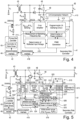
- Fig. 4 is a block diagram of a power converter 40 according to an embodiment.
- Power converter 40 includes a primary side and a secondary side separated by a transformer 43.
- the primary side receives an input power at an input voltage V in
- the secondary side outputs an output power at an output voltage V out .
- a primary side switch 44 is provided, controlled by a controller and gate driver 45 of a primary side controller 42.
- a current through a primary side winding of transformer 43 may be selectively switched on or off, which in turn induces a current on the secondary side of power converter 40 and therefore transfers power to the secondary side.
- primary side switch 44 is controlled by a pulse width modulated (PWM) signal, which is generated by a secondary side controller 41 and communicated to primary side controller 42 via communication interfaces 418, 46.
- PWM pulse width modulated
- Communication interfaces 46, 418 may be integrated in controllers 42, 41, respectively (for example in a respective ASIC), or may be provided externally to controllers 42, 41, for example as an optocoupler.
- communication interface 46 may include a phototransistor
- communication interface 418 may include a light emitting diode (LED), to transfer information regarding the PWM signal from secondary side controller 41 to primary side controller 42.
- LED light emitting diode
- Other conventional communication techniques maintaining the galvanic isolation provided by transformer 43 between primary and secondary side may also be used, for example capacitive or inductive coupling, which may use capacitors or inductors integrated in the respective controllers 42, 41 or external to controllers 42, 41. While in some implementation on the primary side a shunt resistor R CS may be provided for measuring a drain current of primary side switch 44, this is not required for the power limitation techniques discussed herein, but if desired may be used for other purposes in power converter 40.
- the power provided by the transformer 43 is filtered by a filter 48, for example a simple capacitor, and rectified by a rectifier element 47 represented as a diode in Fig. 4 .
- a filter 48 for example a simple capacitor
- a rectifier element 47 represented as a diode in Fig. 4 .
- SR transistor synchronous rectifier transistor
- Secondary side controller 41 receives a feedforward current I FF at a terminal ZCDS and the output voltage V out prior to filtering at a terminal VCCS. Furthermore, the output voltage V out is divided by a voltage divider 49 including resistors R A and R B to be received at a terminal FB.
- the signal at ZCDS is representative of a voltage at rectifier element 47, for example a drain voltage V SR,drain of a synchronous rectifier transistor used as rectifier element 47, and the signal received at VCCS is representative for Vout. These two quantities are sensed in a block 411.
- the voltage V SR,drain furthermore is an example for a signal indicative of the switching frequency f sw of primary side switch 44, as it exhibits a waviness or periodicity corresponding to f SW .
- This switching frequency f SW is determined in block 414.
- the reflected input voltage V in,sec is determined, as will be explained further below using examples.
- V out in a regulated state is a constant needed for determining the reflected input voltage, as further explained below with reference to Fig. 5 .
- a power limit is determined, as will be explained further below.
- An error amplifier 412 receives the divided output signal via terminal FB and compares it with a reference voltage serving as a target value.
- the output of error amplifier 412 is representative of a deviation of the output voltage from the target value. In conventional systems, this value may be directly used for the generation of the PWM control signal in block 417, such that when the output voltage gets too low, more power is transferred to the secondary side, and if the output voltage is too high, less power is transferred to the secondary side.
- a programmable error amplifier clamping circuit 413 is programmed to limit an output range of error amplifier 412. As will be shown below in more detail, in this way the power can be limited.
- the PWM control signal in Fig. 4 is generated based on the limited error amplifier output signal and the reflected input voltage by PWM generation block 417 and communicated to primary side controller and gate driver 45 via communication interfaces 418, 46 as already explained above, such that primary side switch 44 is controlled based thereon.
- the reflected input voltage is a measure of the input voltage, and in this way the input voltage which is provided on the primary side can be measured at the secondary side.
- a regulator e.g. any combination of proportional (P), integral (I) and derivative (D) regulator
- V EA voltage output by error amplifier 412, labelled V EA in the following, influences the input power drawn by converter 40.
- I pri is the primary side current
- f SW is the switching frequency of a primary side switch
- V in,pri is the peak value of the primary side voltage
- t mag is the magnetization-time of transformer 43, which is approximately the on-time of primary side switch 44.
- V in,pri is the primary side input voltage
- k FF is a constant determining the charging amount
- R ZCDS is the resistance of resistor R ZCDS of Fig. 4
- N 1 /N 2 is the turns ratio of transformer 43.
- L is the primary side inductance of transformer 43.
- Vbulk essentially corresponds to Vpri,pk.
- Vbulk is the rectified AC input voltage after a bridge rectifier rectifying e.g. an AC mains voltage and which is stabilized by the so-called bulk capacitance. Depending on load the bulk voltage is either close to the peak AC voltage (for very low loads and big bulk capacitances) or it may have a significant ripple (for high load or small bulk capacitances).
- a low line condition may be used as a reference level for the power limit, i.e. a condition with low input voltage.
- Power converters are usually limited in the power which they can deliver to the output at low line conditions.
- high line conditions i.e. high input voltage
- power converters usually can provide much higher power to the output.
- this limit may be set based on the lowest level all across line voltages which usually occurs at the lowest line condition, i.e. lowest input voltage.
- V EA,0 , f SW,0 , V in,0 and t PWM,on,0 i.e. parameters corresponding to this reference level for the power limit are given.
- These parameters for a given system may for example be programmed in eFuses, read only memories (ROM) or other types of storage.
- V in,sec is the reflected input voltage
- k ref,power is a system constant.
- k ref,power is defined as f SW,0 ⁇ V EA,0 ⁇ V bulk,0 ⁇ t PWM,on,0 .
- the turns ratio N 2 /N 1 and k ref,power may be stored in the device. It should be noted that k ref,power is essentially independent of a specific design implementation. This means that e.g. a power converter manufacturer can scale the power capability of the power converter by e.g.
- k ref,power is set based on parameters at some preselected operation point (e.g. low line condition as explained above), such that is independent from such circuit component variations.
- k ref,power may be programmable and may for example be set to different values depending on output voltage.
- the limit for the error amplifier voltage may be set based on the switching frequency f SW or switching period T SW , which is the inverse of the switching frequency.
- V in,sec ⁇ t PWM.on may be explicitly determined for the above formula.
- V in,sec may be determined in block 416 based on the signals at terminals ZCDS and VCCS in secondary side controller 41.
- t PWM,on may be obtained from the PWM control signal generated by block 417.
- V in,sec ⁇ t PWM,on also referred to as voltage-time-integral
- V EA,limit may then be used for setting the clamping limits in block 413 in Fig. 4 .
- a secondary side controller like controller 10 of Fig. 1 or secondary side controller 41 of Fig. 4 may have digital and analog components.
- Fig. 5 illustrates a power converter 50 including a secondary side controller 51 with a mostly digital implementation.
- Components corresponding to components already described with reference to Fig. 4 bear the same reference numerals and will not be described in detail again.
- rectifier element 47 of Fig. 4 is implemented as a synchronous rectifier transistor 530 with a freewheeling diode 570.
- Synchronous rectifier (SR) transistor 530 is controlled by an SR gate driver 520.
- the switching of transistor 530 may performed in a conventional manner, as known to the skilled person for SR transistors, corresponding to the switching of primary side switch 44.
- the compensation network 410 in the embodiment of Fig. 5 is implemented as a network 510 coupled to ground as shown. This, together with error amplifier 512, forms a PI controller
- a voltage sensing block 511 For measuring the voltage at terminals ZCDS and VCCS, in a voltage sensing block 511 two analog-to-digital converters 521, 522 are provided, to generate respective digital values. The following processing of these digital values is implemented in the digital domain, and even if for clarity separate blocks are shown, any kind of digital signal processing may be used to implement the respective functionality.
- a subtractor 523 For determining the reflected input voltage in V in,sec in a block 516, a subtractor 523 is used determining the difference between the output values of analog-to-digital converters 521, 522.
- the signal output by analog-to-digital converter 521 is provided to a counter 524 which may for example count times between the reaching of threshold values, thus determining a period length of the signal.
- PWM generation block 517 generates a PWM control signal.
- the PWM control causes an on-time of primary side switch 44.
- a power limitation block 515 receives the on-time from PWM generation block 517, the input reflected input voltage V in,sec from block 516 and the switching frequency or switching period from block 514, and determines a power limit as discussed above with respect to equation (5) in form of a limit for an error voltage. This limit is provided to a clamping circuit 513 via a digital-to-analog converter 527 to set minimum and maximum clamping values 528, 529, respectively, which may be the negative and positive version of the value determined according to the above equation (5).
- V EA,limit V EA , 0 f sw , 0 f sw
- the limit for V EA may also, as an alternative, be digitally provided directly to PWM generation block 517, which receives the error voltage V EA via an analog-to-digital converter 526 and may limit the voltage digitally to the value V EA,limit in case it exceeds it in the course of the PWM signal generation directly.
- the determination of the power limitation uses values stored in a ROM 519 (for example provided by eFuses), for example the above values k ref,power and the turns ratio N 2 /N 1 .
- An error amplifier block 512 receives the feedback voltage from voltage divider 49 and amplifies a difference between the feedback voltage and a reference voltage V ref,EA in a differential amplifier 531.
- the signal output by differential amplifier 531 controls the gate of a transistor 532 which may be operated in a linear regime supplied by a current source 533, to provide the error voltage V EA .
- This error voltage is then clamped in programmable EA clamping circuit 513.
- the PWM signal generated is then provided to primary side controller 42 as already explained with reference to Fig. 4 via communication interfaces 418, 46.
- Fig. 6 shows a power converter 60 including a predominantly analog implementation of secondary side controller 61.
- the compensation network is implemented as an RC network feeding an output at terminal EA back to terminal FB.
- This similar to compensation network 510 of Fig. 5 , forms a PI controller.
- a high pass filter e.g. RC series coupling, may be provided between the output voltage Vout and terminal FB.
- network 510 is coupled to ground, whereas in Fig. 6 it is coupled to terminal FB. Both possibilities may be used, depending on the implementation of the corresponding error amplifier.
- the voltage across resistor R ZCDS is regulated to approximately equal the reflected input voltage because the voltage at terminal ZCDS is regulated to approximately the output voltage V out by Vout clamp 632, where terminal VCCS is coupled to a gate terminal of a transistor as shown.
- V clamp and a current I ZCDS , which is transformed to a feedforward current I FF using a controllable current source 640 in PWM generation block 617 and essentially a switched current mirror including transistors 634, 635 with a switch 637 and a capacitor 636 and a transistor 638 coupled as shown, with a ratio between currents of 1:k FF .
- Switch 637 and capacitor 636 essentially provide a sample-and-hold functionality.
- the reflected input voltage can only be sensed on the ZCDS terminal while primary side switch 44 is closed.
- this sample-and-hold functionality in the embodiment of Fig. 6 is used to sample the information provided by the voltage V clamp during (a part of) the primary side pulse and holds this constant during the remaining time.
- the current I FF is therefore representative of the reflected input voltage.
- the sample-and-hold functionality provided by switch 637 and capacitor 636 may be omitted, and capacitor 642 may be charged with the current I FF during times when primary side switch 44 is switched on.
- the thus generated current I FF charges capacitor 624 with the above-mentioned capacitance C PWM for generation of the pulse width modulated signal using a comparator 641, which compares the voltage at capacitor 624 to the output voltage V EA of already discussed error amplifier 512, as clamped by block 513 as also already discussed.
- V EA,limit in a block 615 on the one hand the switching frequency f sw is determined in block 614, using a counter 624, similar to the use of counter 524 of block 514 in Fig. 5
- counter 624 may also count the signal output by comparator 641.
- V EA,limit optionally in a block 644 an analog-to-digital converter 645 digitizes a value corresponding to I FF to serve as measure for the reflected input voltage, and a counter 646 measures the on-time t on,PWM of the PWM Signal, and provide the respective values together with values stored in a ROM (k ref,power , N 2 /N 1 ) or other memory to block 647.
- a ROM k ref,power , N 2 /N 1
- the product of the reflected input voltage and the on-time may be assumed to be a constant and need not be measured.
- the thus determined limit value for the error amplifier voltage V EA,limit is converted to an analog value by a digital-to-analog converter 648 and used for the clamping of the error amplifier voltage in block 513 as described.
- the reference voltage Vref,EA fed to error amplifier 531 may be modified to limit the difference seen by error amplifier 531.
- capacitor 624 may be tuneable, and by tuning capacitor the capacitance value CPWM also a limitation may be obtained, see equation (2) above, which shows that a reduction of CPWM leads to a reduction of power
- V EA V EA ⁇ C PWM / I FF .
- a maximum voltage to which capacitor 642 is charged may be limited.
- the current provided for charging capacitor 624 may be modified by controlling tuneable current source 640 as a modification of the charging current may influence the charging in a similar manner as a modification of the capacitance, but with an inverse function (as I FF is in the denominator for determining the pulse duration as explained above).
- FIGS 7 and 8 show signal diagrams for further illustration.
- Fig. 7 illustrates how the time voltage integral mentioned above, i.e. V in,sec x t PWM,on , remains essentially constant.
- V SR,drain at a drain of transistor 530, as measured at ZCDS is shown, which is the sum of V in,sec and V out .
- a curve 70 shows a first case
- a curve 71 shows a second case with a lower voltage.
- the feedforward current I FF is shown, in a curve 72 for the first case and 73 for the second case.
- the maximum value I FF,max of I FF is higher than for the second case.
- Fig. 8 illustrates the effects of the limitation of the voltage V EA .
- Fig. 8 shows the same quantities as discussed with reference to Fig. 7 , i.e. on top of the graphs of Fig. 8 the drain voltage V SR,drain is shown in a curve 80, in a curve 81 the feedforward current I FF is shown, and in a curve 83 the PWM voltage at capacitor 642 is shown.
- a curve 82 shows the limit of V EA , which changes from a first value V EA,limitl to a second value V EA,limit2 .
- the output voltage of the error amplifier reaches this limit in both cases, i.e. that the value output by block 513 to the negative input of comparator 641 corresponds to the limit value and not to a value generated by block 512.
- Fig. 9 illustrates a power converter 90 according to a further embodiment, which is a variation of power converter 60 of Fig. 6 . Again, similar elements bear the same reference numerals and will not be discussed again.
- a primary side controller 92 of power converter 90 includes primary side switch 44.
- Primary side controller 92 receives an output signal pwm_out from a secondary side controller 91, in particular a block 951 thereof, which generates the signal based on the output signal of comparator 641 already discussed.
- a comparator 952 may be used to protect primary side switch 44 and transformer 43 from excessively high current, which may occur in case of a shortened transformer winding or other failures, by comparing the voltage at a terminal CSP to a reference voltage as shown.
- a resistance R S,pri couples primary side controller 92 to ground.
- a control block 951 controls primary side switch 44 in the same manner as discussed before for controller and gate driver 45 of primary side controller 42.
- capacitor 942 is depicted as non-adjustable, although an adjustable capacitor may also be provided.
- the signal provided from capacitor 924 to the positive input of comparator 641 is additionally provided to a clamping device formed by a comparator 950.
- Comparator 950 protects capacitor 942 against excessive charging and may also be used to limit the pulse width to a configurable level V ref,clhs . Setting of the clamping values 528 and 529 is not explicitly shown in Fig. 9 and may be performed as in any of the previously discussed embodiments.
- signals EAcomp_out and hlclamp_out may also be output to further entities and may for example be used for monitoring purposes. For example, based on these signals a digital signal processing logic may detect if the controller and hence the power converter operates normally without power limitation or operates with power limitation.
- PWM control logic 951 may comprise logic elements like a latch and logic gates to process the output signal of comparators 641 to generate a PWM control signal essentially as already indicated with respect to Fig. 7 , i.e. a signal that for each switching cycle is on while the voltage at capacitor 942 is below the error amplifier voltage V EA , and low afterwards, as indicated by comparator 641.
- a secondary side controller generates a PWM control signal, which is transmitted to a primary side controller for operation of a primary side switch. Due to the communication necessary, there is some delay until the effects of a modified PWM signal is seen again on the secondary side. For very short on-times, these propagation delays may contribute to a noticeable difference between on-time and magnetization time of transformer 43 due to a corresponding overshoot of the primary peak current. In some embodiments, to accommodate such cases, a propagation delay compensation is employed.
- Vin,min and Vin,max are the minimum and maximum input voltages respectively, which are known and specified for each integrated circuit and independent of the actual system dimensioning and implementation.
- the propagation delay compensation value for the error amplifier limitation in case of a digital calculation, may be programmable or selectable. The value is not entirely independent from the used components, as the propagation delay may depend on the gate capacitance of the employed transistor. The delay may be measured using a test signal, and then V EA,PDC , which is a voltage used for compensation, may be selected appropriately.
Landscapes
- Engineering & Computer Science (AREA)
- Power Engineering (AREA)
- Dc-Dc Converters (AREA)
Priority Applications (2)
| Application Number | Priority Date | Filing Date | Title |
|---|---|---|---|
| EP23161148.4A EP4429094A1 (de) | 2023-03-10 | 2023-03-10 | Stromrichtersteuergerät, stromrichter und verfahren zum betrieb eines stromrichters |
| CN202410259711.4A CN118631064A (zh) | 2023-03-10 | 2024-03-07 | 功率转换器的次级侧控制器、功率转换器和操作功率转换器的方法 |
Applications Claiming Priority (1)
| Application Number | Priority Date | Filing Date | Title |
|---|---|---|---|
| EP23161148.4A EP4429094A1 (de) | 2023-03-10 | 2023-03-10 | Stromrichtersteuergerät, stromrichter und verfahren zum betrieb eines stromrichters |
Publications (1)
| Publication Number | Publication Date |
|---|---|
| EP4429094A1 true EP4429094A1 (de) | 2024-09-11 |
Family
ID=85570194
Family Applications (1)
| Application Number | Title | Priority Date | Filing Date |
|---|---|---|---|
| EP23161148.4A Pending EP4429094A1 (de) | 2023-03-10 | 2023-03-10 | Stromrichtersteuergerät, stromrichter und verfahren zum betrieb eines stromrichters |
Country Status (2)
| Country | Link |
|---|---|
| EP (1) | EP4429094A1 (de) |
| CN (1) | CN118631064A (de) |
Citations (6)
| Publication number | Priority date | Publication date | Assignee | Title |
|---|---|---|---|---|
| US20150280573A1 (en) * | 2014-04-01 | 2015-10-01 | Infineon Technologies Austria Ag | System and Method for a Switched-Mode Power Supply |
| WO2017089120A1 (en) * | 2015-11-26 | 2017-06-01 | Philips Lighting Holding B.V. | A driver circuit |
| US10193458B2 (en) * | 2014-11-20 | 2019-01-29 | Microchip Technology Incorporated | Start-up controller for a power converter |
| WO2019168399A2 (en) * | 2018-02-28 | 2019-09-06 | Eldolab Holding B.V. | Power converter for led |
| US10651753B1 (en) * | 2019-06-26 | 2020-05-12 | Cypress Semiconductor Corporation | Accurate valley detection for secondary controlled flyback converter |
| US20220131457A1 (en) * | 2020-10-28 | 2022-04-28 | Inno-Tech Co., Ltd. | Power control system of adaptive control of turn on time |
-
2023
- 2023-03-10 EP EP23161148.4A patent/EP4429094A1/de active Pending
-
2024
- 2024-03-07 CN CN202410259711.4A patent/CN118631064A/zh active Pending
Patent Citations (6)
| Publication number | Priority date | Publication date | Assignee | Title |
|---|---|---|---|---|
| US20150280573A1 (en) * | 2014-04-01 | 2015-10-01 | Infineon Technologies Austria Ag | System and Method for a Switched-Mode Power Supply |
| US10193458B2 (en) * | 2014-11-20 | 2019-01-29 | Microchip Technology Incorporated | Start-up controller for a power converter |
| WO2017089120A1 (en) * | 2015-11-26 | 2017-06-01 | Philips Lighting Holding B.V. | A driver circuit |
| WO2019168399A2 (en) * | 2018-02-28 | 2019-09-06 | Eldolab Holding B.V. | Power converter for led |
| US10651753B1 (en) * | 2019-06-26 | 2020-05-12 | Cypress Semiconductor Corporation | Accurate valley detection for secondary controlled flyback converter |
| US20220131457A1 (en) * | 2020-10-28 | 2022-04-28 | Inno-Tech Co., Ltd. | Power control system of adaptive control of turn on time |
Also Published As
| Publication number | Publication date |
|---|---|
| CN118631064A (zh) | 2024-09-10 |
Similar Documents
| Publication | Publication Date | Title |
|---|---|---|
| JP5693877B2 (ja) | 電源のためのコントローラ、電源、および電源を制御する方法 | |
| US11005378B2 (en) | Operating a flyback converter using a signal indicative of a resonant tank current of the flyback converter | |
| US11128211B2 (en) | Method for driving an electronic switch in a power converter circuit and control circuit | |
| US9647562B2 (en) | Power conversion with switch turn-off delay time compensation | |
| EP2621069B1 (de) | Sperrwandler mit primärseitiger Ausgangsspannungserfassung und Überspannungsschutz im Betrieb mit niedriger Last | |
| US6958920B2 (en) | Switching power converter and method of controlling output voltage thereof using predictive sensing of magnetic flux | |
| US10778103B2 (en) | Digitally compensated current sensing protection | |
| US11955894B2 (en) | Quasi-resonant auto-tuning controller | |
| US9077253B2 (en) | Control integrated circuit for a power transistor of a switching current regulator | |
| US20150103566A1 (en) | Systems and Methods of CCM Primary-Side Regulation | |
| GB2451088A (en) | Regulating the output of a forward power converter | |
| US11990843B2 (en) | Methods and circuits for sensing isolated power converter output voltage across the isolation barrier | |
| US11233456B2 (en) | Methods and systems of operating power converters | |
| US20040264216A1 (en) | Switching power converter and method of controlling output voltage thereof using predictive sensing of magnetic flux | |
| US11616445B2 (en) | Method for driving a switch in a power converter, drive circuit and power converter | |
| EP4429094A1 (de) | Stromrichtersteuergerät, stromrichter und verfahren zum betrieb eines stromrichters | |
| US12155312B2 (en) | Power converter controller, power converter and method for operating control of a power stage based on an intermediate voltage with respect to a threshold value determined from a turns ratio of a transformer | |
| KR100848685B1 (ko) | 프라이머리 레규레이션 방식의 에스엠피에스의 정전압 오차보정회로 | |
| US12132383B2 (en) | Current sampling in converter circuits |
Legal Events
| Date | Code | Title | Description |
|---|---|---|---|
| PUAI | Public reference made under article 153(3) epc to a published international application that has entered the european phase |
Free format text: ORIGINAL CODE: 0009012 |
|
| STAA | Information on the status of an ep patent application or granted ep patent |
Free format text: STATUS: THE APPLICATION HAS BEEN PUBLISHED |
|
| AK | Designated contracting states |
Kind code of ref document: A1 Designated state(s): AL AT BE BG CH CY CZ DE DK EE ES FI FR GB GR HR HU IE IS IT LI LT LU LV MC ME MK MT NL NO PL PT RO RS SE SI SK SM TR |
|
| STAA | Information on the status of an ep patent application or granted ep patent |
Free format text: STATUS: REQUEST FOR EXAMINATION WAS MADE |
|
| 17P | Request for examination filed |
Effective date: 20250311 |
|
| STAA | Information on the status of an ep patent application or granted ep patent |
Free format text: STATUS: EXAMINATION IS IN PROGRESS |
|
| 17Q | First examination report despatched |
Effective date: 20250702 |