EP4431950A1 - Widerstandsanordnung, stromsensoranordnung und verfahren zum bestimmen einer temperatur der widerstandsanordnung - Google Patents
Widerstandsanordnung, stromsensoranordnung und verfahren zum bestimmen einer temperatur der widerstandsanordnung Download PDFInfo
- Publication number
- EP4431950A1 EP4431950A1 EP23161743.2A EP23161743A EP4431950A1 EP 4431950 A1 EP4431950 A1 EP 4431950A1 EP 23161743 A EP23161743 A EP 23161743A EP 4431950 A1 EP4431950 A1 EP 4431950A1
- Authority
- EP
- European Patent Office
- Prior art keywords
- resistance
- temperature
- section
- electrically conductive
- resistor arrangement
- Prior art date
- Legal status (The legal status is an assumption and is not a legal conclusion. Google has not performed a legal analysis and makes no representation as to the accuracy of the status listed.)
- Granted
Links
Images


Classifications
-
- G—PHYSICS
- G01—MEASURING; TESTING
- G01R—MEASURING ELECTRIC VARIABLES; MEASURING MAGNETIC VARIABLES
- G01R1/00—Details of instruments or arrangements of the types included in groups G01R5/00 - G01R13/00 and G01R31/00
- G01R1/20—Modifications of basic electric elements for use in electric measuring instruments; Structural combinations of such elements with such instruments
- G01R1/203—Resistors used for electric measuring, e.g. decade resistors standards, resistors for comparators, series resistors, shunts
-
- G—PHYSICS
- G01—MEASURING; TESTING
- G01R—MEASURING ELECTRIC VARIABLES; MEASURING MAGNETIC VARIABLES
- G01R1/00—Details of instruments or arrangements of the types included in groups G01R5/00 - G01R13/00 and G01R31/00
- G01R1/44—Modifications of instruments for temperature compensation
-
- G—PHYSICS
- G01—MEASURING; TESTING
- G01R—MEASURING ELECTRIC VARIABLES; MEASURING MAGNETIC VARIABLES
- G01R19/00—Arrangements for measuring currents or voltages or for indicating presence or sign thereof
- G01R19/0092—Measuring current only
-
- H—ELECTRICITY
- H01—ELECTRIC ELEMENTS
- H01C—RESISTORS
- H01C7/00—Non-adjustable resistors formed as one or more layers or coatings; Non-adjustable resistors made from powdered conducting material or powdered semi-conducting material with or without insulating material
- H01C7/06—Non-adjustable resistors formed as one or more layers or coatings; Non-adjustable resistors made from powdered conducting material or powdered semi-conducting material with or without insulating material including means to minimise changes in resistance with changes in temperature
-
- G—PHYSICS
- G01—MEASURING; TESTING
- G01R—MEASURING ELECTRIC VARIABLES; MEASURING MAGNETIC VARIABLES
- G01R35/00—Testing or calibrating of apparatus covered by the other groups of this subclass
- G01R35/005—Calibrating; Standards or reference devices, e.g. voltage or resistance standards, "golden" references
-
- G—PHYSICS
- G01—MEASURING; TESTING
- G01R—MEASURING ELECTRIC VARIABLES; MEASURING MAGNETIC VARIABLES
- G01R35/00—Testing or calibrating of apparatus covered by the other groups of this subclass
- G01R35/02—Testing or calibrating of apparatus covered by the other groups of this subclass of auxiliary devices, e.g. of instrument transformers according to prescribed transformation ratio, phase angle, or wattage rating
-
- H—ELECTRICITY
- H01—ELECTRIC ELEMENTS
- H01C—RESISTORS
- H01C13/00—Resistors not provided for elsewhere
- H01C13/02—Structural combinations of resistors
Definitions
- the present disclosure relates to a resistor arrangement, a current sensor assembly comprising the resistor arrangement, and a method for determining a temperature of the resistor arrangement.
- measuring resistors are used which are connected in series with a component to be monitored, whereby a current to be measured can be determined from the voltage dropping across the measuring resistor, which is often also referred to as a shunt resistor or shunt for short.
- Correct and reliable current measurement is particularly important, for example, in a battery management system of a hybrid or electric vehicle or for monitoring a fuel cell device.
- Such a low-resistance measuring resistor as a shunt with approximately 10 - 50 ⁇ Ohm can be made from a longitudinally welded composite material strip. This is known, for example, from EP 0 605 800 A1 .
- the composite material is produced from three material strips by joining the individual metal strips to each other, each via a longitudinal seam, by an electron beam or laser welding process.
- the redundancy of the current measurement which is necessary to achieve the safety level ASIL C, can be achieved by the combination of different sensors, i.e. the simultaneous acquisition of two completely different measurement signals, for example by a voltage measurement at a shunt resistor of known size and by a measurement of the Hall voltage on an current-carrying conductor in a magnetic field.
- this setup is associated with relatively high costs, also because the integration is low and many components with a correspondingly high installation space requirement are needed.
- the redundancy in the measured value acquisition can also be achieved by connecting a second shunt resistor in series to the first shunt resistor, instead of using the Hall voltage measurement, and by performing an independent voltage measurement on each of the two shunt resistors of the double shunt thus formed to determine the current strength. By comparing the two measurements, it can then be determined whether the measurements are plausible or whether there is an error.
- the double shunt thus enables the diagnosis of "single point faults", namely of drift, change in resistance, or de-contacting of individual measurement taps. It further offers better diagnosis options for the shunt electronics by means of a plausibility check of the measurement by two shunt elements integrated in one component.
- the structure of the current measurement using a double shunt is simpler and less expensive than a current measurement using a single shunt and an additional Hall sensor.
- the inventors of the present invention have recognized that there is still a need to provide a resistance arrangement and a corresponding current sensor assembly improving performance and reliability of the sensor output and facilitating the manufacturing process, thereby overcoming, or at least substantially reducing the above mentioned problems and drawbacks.
- the present invention is based on the idea of directly integrating a predefined resistance as a second resistance element in one of the two conductive connection elements, which are welded to a first resistance element to form the resistor arrangement, by geometrically forming a well-defined resistance in the respective conductive connection element.
- the integration of the predefined resistance into one of the two conductive connection elements allows to improve the temperature determination of the resistor arrangement and specifically of the first resistor element in order to improve the accuracy of the current determination, since the temperature can be directly sensed by the resistance section integrated into the conductive connection elements.
- a resistor arrangement comprises a first electrically conductive connection element and a second electrically conductive connection element, which are formed of a first electrically conductive material having a first specific electrical conductivity, a first resistance element formed of a first resistance material having a second specific electrical conductivity, which is lower than the first specific electrical conductivity, wherein the first resistance element is connected with a first end to the first electrically conductive connection element and with a second end to the second electrically conductive connection element.
- the first electrically conductive connection element comprises a terminal connection section, which is configured to be electrically connected to an external conductor of an electrical circuit, an intermediate connection section, which is connected with the first end of the resistance element, and a resistance section, which is arranged in between the terminal connection section and the intermediate section.
- the first resistance element has a first predefined resistance
- the resistance section of the first electrically conductive connection element has a second predefined resistance.
- the resistor arrangement can reduce the total resistance introduced in an electric circuit for measuring a current, while the resistor arrangement allows for an enhancement of the temperature determination and a redundant current measurement.
- the first resistance element and the resistance section of the first electrically conductive connection element are specifically made of different materials, which in particular may have different chemical compositions, wherein in particular CuMn10Ni4 and CuMn12Ni2 and CuMn14Ni2 and CuZn15Mn150AI can be named as examples of the first resistance material forming the first resistance element, and wherein in particular copper (Cu) or aluminum (Al) can be named as examples of the first electrically conductive material forming the resistance section.
- predefined resistance can refer to a nominal value of the resistance the respective resistance element or of the resistance section, which is includes an uncertainty due to manufacturing tolerances, or can refer to a calibrated value, which has been individually determined for the respective resistance element or resistance section after manufacturing the resistor arrangement.
- the second predefined resistance is smaller than the first predefined resistance.
- the resistor arrangement may further comprise a first measuring contact pair for measuring a first electrical voltage dropping across the first resistance element and a second measuring contact pair for measuring a second electrical voltage dropping across the resistance section of the first electrically conductive connection element, wherein a first measuring contact from the first measuring contact pair and a second measuring contact from the second measuring contact pair are arranged on the intermediate connection section of the first electrically conductive connection element.
- the resistance section may include a constriction, which has a predetermined geometrical shape.
- the first electrically conductive element may be punched, stamped or cut out in order to a constriction with a predefined shape, which provides the second predefined resistance between a measuring contact pair.
- the resistance section may be formed as a region of the first electrically conductive element between a measuring contact pair, which has a total resistance corresponding to the second predefined resistance.
- the first electrically conductive connection element may be formed in such a way that a minimum thickness of the resistance section is smaller than a minimum thickness of the terminal connection section and a minimum thickness of the intermediate connection section and/or that a minimum width of the resistance section is smaller than a minimum width of the terminal connection section and a minimum width of the intermediate connection section.
- This configurations enhances the possibilities to adjust the second predefined resistance and also offers advantages when mounting the resistor arrangement on a PCB (printed circuit board), for example, or when soldering the resistor arrangement to another circuit component.
- connection section of the first electrically conductive connection element and the second electrically conductive connection element comprise connection means for integrating the resistor arrangement into an electric circuit.
- a current sensor assembly which comprises the resistor arrangement according to one of the aspects, a first voltage tap for measuring a first electrical voltage dropping across the first resistance element, a second voltage tap for measuring a second electrical voltage dropping across the resistance section, and a measuring circuit, which is configured to measure the first electrical voltage and the second electrical voltage.
- the measuring circuit may be configured to perform the measurement of the first electrical voltage and of the second electrical voltage independently from one another, so that a failure of one of the two measuring chains can be recognized by comparing the two measurements.
- the current sensor assembly may further comprise a storage, which is configured to store a temperature coefficient of the first electrically conductive material, and a processing circuit, which is configured to determine a first current value of a current flowing through the resistor arrangement based on the first electrical voltage and the first predefined resistance, and a temperature of the resistance section of the first electrically conductive connection element based on the first current value, the second electrical voltage and the stored temperature coefficient of the first electrically conductive material.
- a storage which is configured to store a temperature coefficient of the first electrically conductive material
- a processing circuit which is configured to determine a first current value of a current flowing through the resistor arrangement based on the first electrical voltage and the first predefined resistance, and a temperature of the resistance section of the first electrically conductive connection element based on the first current value, the second electrical voltage and the stored temperature coefficient of the first electrically conductive material.
- a linear temperature coefficient e.g.
- the temperature of the resistance section can be determined from the current flowing through the resistance section. This allows for directly measuring the temperature of the resistor arrangement with an element integrated into the resistance arrangement, so that the need for attaching an external temperature sensor is dispensed.
- the current sensor assembly may further comprise a temperature sensor attached to the resistor arrangement, which is configured to measure a second temperature of the resistor arrangement, wherein the processing circuit may be further configured to compare the determined temperature of the resistance section to the second temperature, which is measured with the temperature sensor.
- the second temperature may for example be measured by an NTC or another kind of resistance temperature sensor attached to the resistor arrangement.
- the processing circuit may be further configured to determine a second current value of the current flowing through the resistor arrangement based on the second electrical voltage and the second predefined resistance, and to compare the second current value to the first current value, in order to check consistency of the determined current values and to detect or diagnose measurement faults and/or "single point faults".
- the method comprises the steps of acquiring, from a measuring circuit, measurement values of a measurement of a first electrical voltage dropping across the first resistance element and of a measurement of a second electrical voltage dropping across the resistance section of the first electrically conductive connection element, determining a first current value of a current flowing through the resistor arrangement based on the first electrical voltage and the first predefined resistance, and determining a temperature of the resistance section of the first electrically conductive connection element based on the first current value, the second electrical voltage and a stored temperature coefficient of the first electrically conductive material.
- This method may be carried out for example by the processing circuit of the current sensor assembly, which can be a controller of the resistor arrangement provided on a circuit board attached to the resistor arrangement, but can also be an external controller, like a central controller of a battery management system (BMS) or an electronic control unit (ECU) of an electric vehicle or a hybrid electrical vehicle, which control the operation of electronic components in the electric circuit, in which the resistor arrangement is used.
- BMS battery management system
- ECU electronice control unit
- the resistance section is formed of first electrically conductive material having a linear temperature coefficient (e.g. copper or aluminum)
- the resistance section is directly thermally coupled with the resistance element the method allows for a more precise and dynamic determination of the temperature of the first resistance element. Hence the accuracy of a TCR (temperature coefficient ratio) correction of the resistance of the first resistance element can be greatly enhanced.
- the determination of the temperature of the resistance section is iteratively repeated until the determined temperature converges.
- the temperature coefficient of the material, from which the first resistance element is formed is a few orders of magnitude smaller than the temperature coefficient of the material, from which the resistance section of the first electrically conductive connection element is formed. Accordingly, after setting an arbitrary estimated starting temperature for determining the temperature of the resistance, when iteratively solving the above equations (2) and (3), the determined temperature converges to the actual temperature of the resistance section.
- the method may further comprise a step of comparing the determined temperature of the resistance section with a second temperature, which is measured with a temperature sensor attached to the resistor arrangement.
- the second temperature may for example be measured by a temperature sensor, like an NTC or other resistance temperature sensor, which is attached to the first electrically conductive connection element or to the second electrically conductive connection element.
- the method may further comprise a calibration step of determining the resistance of the resistance section at a defined calibration temperature and a storing step of storing the determined resistance of the resistance section at the defined calibration temperature in a storage.
- the method may further comprise a step of determining a second current value of the current flowing through the resistor arrangement based on the second electrical voltage and the second predefined resistance, and a step of comparing the second current value to the first current value in order to check consistency of the determined current values and to detect or diagnose measurement faults and/or "single point faults".
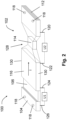
- Fig. 1 shows a resistor arrangement 100, which comprises a first electrically conductive connection element 102, which can be also referred to as a first busbar, and a second electrically conductive connection element 104, which can be also referred to as a second busbar.
- the first electrically conductive connection element 102 and the second electrically conductive connection element 104 are formed of a first electrically conductive material with a high specific electrical conductivity, like copper or aluminum.
- a first resistance element 106 which is formed of a first resistance material, which has a lower specific electrical conductivity than the first electrically conductive material, is electrically connected between the first electrically conductive connection element 102 and the second electrically conductive connection element 104.
- the first electrically conductive connection element 102, the second electrically conductive connection element 104 and the first resistance element 106 are preferably formed of metallic strips, which are joint at the connection interfaces 108 and 110, which are preferably arranged at opposed ends of the first resistance element 106, by longitudinal seam welding using an electron beam or laser welding method. In this manner, the three elements are arranged in juxtaposition with each other, wherein the first resistance element 106 is connected with a first end to the first electrically conductive connection element 102 and with a second end to the second electrically conductive connection element 104.
- the first electrically conductive connection element 102 is an integrally formed element, which comprises three regions, namely a first region, which corresponds to a terminal connection section 112, a second region, which corresponds to a resistance section 114, and a third region, which corresponds to an intermediate connection section 116.
- the first electrically conductive connection element 102 and the second electrically conductive connection element 104 each comprise at least one contact element 118.
- the contact elements 118 serve for contacting an external circuit, so as to lead an electrical current I (see the arrow in Fig. 1 ), which is to be measured in the external circuit, through the resistor arrangement 100.
- a direction of the electrical current I is arbitrary.
- the contact elements 118 can for example be formed as cut-outs, which may each be screwed to an external electric component, such as a terminal clamp of a battery or a busbar leading away from the battery.
- the contact elements 118 can for example be formed as welding or soldering joints, which allow to weld or solder the contact elements 118 to the external electric component.
- terminal connection section 112 of the first electrically conductive connection element 102 and the second electrically conductive connection element 104 have at least one contact element 118, but not the intermediate connection section 116, which connects the first resistance element 106 with the resistance section 114 of the first electrically conductive connection element 102.
- the resistance section 114 is a region of the first electrically conductive connection element 102, which serves as a second resistance element of the resistor arrangement 100, and is arranged between the terminal connection section 112 and the intermediate connection section 116. While a first predefined resistance of the first resistance element 106 typically is in a range of 10 - 50 ⁇ Ohm, a second predefined resistance of the resistance section 114 is typically smaller, i.e. preferably below 10 ⁇ Ohm. However, the second predefined resistance may be designed to have a larger resistance, depending on application scenarios, as long as it is smaller, at least at room temperature, than the first predefined resistance. Thereby, it is in particularly favorable that the resistance value of the resistance section 114 is significantly smaller than the resistance value of the first resistance element 106, so as to impose different measuring ranges for the voltage measurement and improve the independence of the measured values.
- the second predefined resistance is defined as a resistance of a region (i.e. the resistance section 114) of the first electrically conductive connection element 102, which is arranged between a pair of measuring contacts, wherein one measuring contact of the pair of measuring contacts is arranged on the terminal connection section 112 and the other measuring contact of the pair of measuring contacts is arranged on the intermediate connection section 116 as will become apparent in more detail from Fig. 2 .
- the second predefined resistance can be a nominal value of the resistance of the resistance section 114, which is includes an uncertainty due to manufacturing tolerances, or can be a calibrated value, which has been individually determined for the resistance section 114 after manufacturing the resistor arrangement 100 at a certain calibration temperature.
- the resistance section 114 may be shaped with a predefined geometry, and may, for example, include a constriction 128 with a maximum cross section smaller than the minimum cross section of the remaining part of the first electrically conductive connection element 102.
- the constriction 128 may be formed, for example, by a tapering cut-out provided on at least one of the side surfaces 130 of the first electrically conductive connection element 102, which extend in parallel to the direction of the current I flowing through the resistor arrangement 100.
- the tapering cut-out may be provided on the two side surfaces 130 as shown in Fig. 1 .
- the tapering cut-out also a rectangle-shaped or circular cut-out is possible.
- the constriction 128 may be formed by reducing the thickness in an area of the resistance section 114 to be lower than a minimum thickness of the remaining parts of the first electrically conductive connection element 102, namely the terminal connection section 112 and the intermediate connection section 116. This makes it possible that the resistance section 114 is located at a distance from a circuit board when the resistor arrangement 100 is attached to this circuit board.
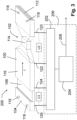
- FIG. 2 shows that a first pair of measuring contacts 124 and 126 for measuring a first electrical voltage U 1 dropping across the first resistance element 106 and a second pair of measuring contacts 120 and 122 for measuring a second electrical voltage U 2 dropping across the resistance section 114 are provided, with the measuring contact 124 from the first pair of measuring contacts and the measuring contact 122 from the second pair of measuring connections being assigned to the intermediate connection section 116.
- the resistance section 114 is defined as the region of the first electrically conductive connection element, which extends between the measuring contacts 120 and 122, so that the second predefined resistance is defined as the resistance measurable between the measuring contacts 120 and 122.
- the voltage measuring contacts 120, 122, 124, and 126 are shown schematically because they may be formed by any suitable contacting technique known in the art.
- the measuring arrangement illustrated in Fig. 2 can be integrated into a current sensor assembly 200, which comprises, in addition to the resistor arrangement 100, a first voltage tap for measuring the first electrical voltage U 1 , and a second voltage tap for measuring the second electrical voltage U 2 and a measuring circuit 202 for measuring the first electrical voltage U 1 and the second electrical voltage U 2 .
- the measuring circuit 202 may for example be a high voltage analog-to-digital converter (HVADC), which serves as an analog-to-digital converter that converts the two analog measurement voltages output by the first voltage tap and the second voltage tap into two digital measurement voltage signals.
- HVADC may comprise dedicated electronics for performing the individual voltage detections in parallel or may comprise electronics for performing the individual voltage detections in a serial order.
- the electronics of the measuring circuit 202 are set up in such a way that the measurement of the first electrical voltage U 1 and the measurement of the second electrical voltage U 2 can take place independently of one another, so that a failure of one of the two measuring chains can be recognized by comparing the two measurements.
- the current sensor assembly 200 as shown in Fig.3 also comprise a processing circuit 204, which may be provided in form of a microcontroller or integrated circuit.
- the measuring circuit 202 and the processing circuit 204 may be mounted on a component carrier, like a (printed) circuit board, to form an assembled circuit 206 as schematically shown in Fig. 3 by the dash-dotted line.
- the assembled circuit may be attached to the resistor arrangement 100.
- electronics components of the assembled circuit are provided by an external controller, like a central controller of a BMS or a vehicle ECU.
- the external controller executes the function of a current determination device, which is configured to carry out the functions and methods, which are described in the following for the processing circuit 204, for example by running a computer program, which is stored in a storage of the external controller and comprises instructions which, when the program is executed by the external controller, cause the external controller to carry out the corresponding methods.
- the processing circuit 204 is configured to acquire measurement values from the measuring circuit 202 by digital communication, and to process the measurement signals in order to generate an output signal 208 and to transmit the output signal 208 to an external controller like a BMS or vehicle ECU.
- the output signal 208 can for example indicate a value of the current I flowing through the resistor arrangement 100, or a value of the temperature T of the resistor arrangement 100 or a part of the resistor arrangement 100.
- the output signal 208 can be a warning signal, which indicates whether at least one of the determined temperature value and the determined current value is outside of a safe operating range.
- Fig. 4 shows a schematic flow chart of a method, which may be performed by the processing circuit 204, for determining the current I flowing through the exemplary resistor arrangement 100.
- the processing circuit 204 receives a first input signal from the measuring circuit 202 indicating information on a measurement value of the first electrical voltage U 1 dropping across the first resistance element 106.
- the first input signal can be received at predetermined time intervals, like once per 1 ⁇ s, once per 1ms, or similar.
- the first input signal can be received in response to an instruction of the processing circuit 204 for the measuring circuit 202 to transmit the information on the measurement value of the first electrical voltage.
- the processing circuit 204 receives a second input signal from the measuring circuit 202 indicating information on a measurement value of the second electrical voltage U 2 dropping across the resistance section 114.
- the second input signal can be received at predetermined time intervals like once per 1 ⁇ s, once per 1ms, or similar.
- the second input signal can be received in response to an instruction of the processing circuit 204 for the measuring circuit 202 to transmit the information on the measurement value of the second electrical voltage.
- a sequence of receiving the first input signal and the second input signal may be switched, or both steps may be performed in parallel.
- the processing circuit 204 then may compare the first current value and the second current value to each other, in order to assess the reliability of the measurement values.
- the processing circuit 204 uses the acquired second voltage U 2 to determine the temperature of the resistance section 114 during the voltage measurement.
- the processing circuit 204 uses the fact that the first electrically conductive material, of which the resistance section 114 as a part of the first electrically conductive connection element 102 is formed, has a linear temperature coefficient ⁇ (e.g. 0,0039 1/K for copper or 0,004 1/K for aluminum) in the operating temperature range of the resistor arrangement 100.
- R 2 (T 0 ): is the resistance of the resistance section 114 determined at the calibration temperature.
- the temperature T used in equation (3) can be estimated by the processing circuit 204 or can be acquired from an external temperature sensor attached to the resistor arrangement as will be described below.
- the resistance section 114 is directly thermally coupled to the first resistance element 106 by the intermediate connection section 116, it can be assumed that the temperature of the first resistance element 106 corresponds to the determined temperature of the resistance section 114, so that the determined temperature of the resistance section 114 can be used to perform an accurate TCR (temperature coefficient ratio) correction of the resistance of the first resistance element 106 and accordingly enhance the accuracy of the determination of the first current value. Accordingly, the specific configuration of the resistor arrangement 100 allows for a determination of the temperature of the first resistance element 106, i.e. a temperature of the resistor arrangement 100 (as the determined temperature of the resistance section 114) without the need for sensing the temperature with an external temperature sensor.
- the above described temperature determination method provides even higher accuracies for the temperature determination, when the resistor arrangement 100 is used during dynamic load profiles, i.e. rapid changes in load and heating.
- the temperature of the first resistor element 106 may additionally sense the temperature of the first resistor element 106 with an external temperature sensor and to compare the additionally sensed temperature to the determined temperature in order to assess the reliability of the temperature determination. For example, a high deviation of the determined temperature from the additionally sensed temperature may hint to a significant drift of the (nominal) resistance of the resistance section 114 and can indicate that a calibration measurement of the resistance of the resistance section 114 should be performed.
- Such a consistency check is not possible with regular resistor arrangements, since the temperature dependency of the temperature coefficient of the first resistance material, of which the resistance elements, are usually formed is too small and follows a non-linear behavior.
- Fig. 7 shows a schematic flow chart of a method for iteratively determining a temperature of the resistance section 114 performed by the processing circuit 204.
- a first step S702 the processing circuit 204 acquires the first electrical voltage U 1 and the second electrical voltage U 2 from the measuring circuit 202 in analogy to step S602 explained above.
- the processing circuit 204 estimates a starting temperature T N and assumes the temperature of the resistance section 114 and of the first resistance element 106 to be T N .
- the staring temperature T N can be a temperature, additionally sensed with an external temperature sensor attached to the resistor arrangement 100, but can also be estimated by the processing circuit 204.
- the processing circuit 204 determines that ⁇ T is not smaller than the predetermined convergence limit (NO in step S710), the processing circuit 204 sets the measured temperature T N+1 as the new starting temperature (S712) and repeats steps S706 - S710 with the new starting temperature T N+1 .
- the processing circuit 204 may perform a calibration of the resistance of the resistance section 114 (i.e. the second predefined resistance) and store the parameters gained from the calibration measurement in the storage of the assembled circuit 206.
- the calibration of the resistance of the resistance section 114 can be performed before the first use of the resistor arrangement 100, or can be performed regularly or in consequence to determining that the calibration becomes necessary.
- the processing circuit 204 may acquire, from the measuring circuit 202, the measurement values of the first voltage U 1 and of the second voltage U 2 measured at a defined calibration temperature To.
- each component of the assembled circuit 206 may be realized by software, hardware, or software in cooperation with hardware. Furthermore, each circuit of the assembled circuit 206 can be realized as a dedicated integrated circuit and the dedicated integrated circuits are assembled to form the assembled circuit. Alternatively, the functionalities of each circuit may be integrated into a common integrated circuit, which forms the assembled circuit. Alternatively, one or more circuits of the assembled circuit may be realized by using general-purpose processors, special-purpose processors, or FPGAs (Field Programmable Gate Array) that can be programmed.
- general-purpose processors special-purpose processors, or FPGAs (Field Programmable Gate Array) that can be programmed.
- resistor arrangement 100 has been exemplarily described to have a single resistance element 106 and a single resistance section 114, a number of resistance elements is not restricted to one. Instead, the same advantages can be achieved when integrating the resistance section 114 into a resistor arrangement with more than one resistance element. Further, it is also possible to integrate more than one resistance section in the resistor arrangement 100, for example respectively one in the different bus-bars (connection elements) 102 and 104 of the resistor arrangement 100.
- REFERENCE NUMERALS 100 resistor arrangement 102, 104 electrically conductive connection elements 106 resistance element 108, 110 connection interfaces 112 terminal connection section 114 resistance section 116 intermediate connection section 118 contact elements 120, 122, 124, 126 measuring contacts 128 constriction 130 side surfaces 200 current sensor assembly 202 measuring circuit 204 processing circuit 206 assembled circuit 208 output signal
Landscapes
- Physics & Mathematics (AREA)
- General Physics & Mathematics (AREA)
- Engineering & Computer Science (AREA)
- Microelectronics & Electronic Packaging (AREA)
- Electromagnetism (AREA)
- Measuring Instrument Details And Bridges, And Automatic Balancing Devices (AREA)
Priority Applications (2)
| Application Number | Priority Date | Filing Date | Title |
|---|---|---|---|
| EP23161743.2A EP4431950B1 (de) | 2023-03-14 | 2023-03-14 | Stromsensoranordnung und verfahren zum bestimmen einer temperatur einer widerstandsanordnung |
| PCT/EP2024/056766 WO2024189125A1 (en) | 2023-03-14 | 2024-03-14 | Resistor arrangement, current sensor assembly, and method for determining a temperature of the resistor arrangement |
Applications Claiming Priority (1)
| Application Number | Priority Date | Filing Date | Title |
|---|---|---|---|
| EP23161743.2A EP4431950B1 (de) | 2023-03-14 | 2023-03-14 | Stromsensoranordnung und verfahren zum bestimmen einer temperatur einer widerstandsanordnung |
Publications (2)
| Publication Number | Publication Date |
|---|---|
| EP4431950A1 true EP4431950A1 (de) | 2024-09-18 |
| EP4431950B1 EP4431950B1 (de) | 2026-04-22 |
Family
ID=85640985
Family Applications (1)
| Application Number | Title | Priority Date | Filing Date |
|---|---|---|---|
| EP23161743.2A Active EP4431950B1 (de) | 2023-03-14 | 2023-03-14 | Stromsensoranordnung und verfahren zum bestimmen einer temperatur einer widerstandsanordnung |
Country Status (2)
| Country | Link |
|---|---|
| EP (1) | EP4431950B1 (de) |
| WO (1) | WO2024189125A1 (de) |
Citations (8)
| Publication number | Priority date | Publication date | Assignee | Title |
|---|---|---|---|---|
| EP0605800A1 (de) | 1992-12-21 | 1994-07-13 | Isabellenhütte Heusler GmbH KG | Verfahren zum Herstellen von Widerständen aus Verbundmaterial und insbesondere nach diesem Verfahren hergestellte Widerstände |
| US20170089955A1 (en) * | 2014-09-25 | 2017-03-30 | Sanyo Electric Co., Ltd. | Electrical current detection device equipped with shunt resistor, and power supply device |
| US20200011905A1 (en) * | 2017-03-03 | 2020-01-09 | Continental Automotive Gmbh | Current sensor with optimized current density distribution, method for determining a load current (as amended) |
| WO2020160979A1 (de) * | 2019-02-05 | 2020-08-13 | Siemens Aktiengesellschaft | Strommessung durch spannungsmessung unter berücksichtigung eines temperaturabhängigen widerstandes |
| DE102019218308A1 (de) * | 2019-11-26 | 2021-05-27 | Continental Automotive Gmbh | Widerstandsbaugruppe für Stromsensor sowie Stromsensor und Verfahren zur Messung eines Batteriestroms |
| EP3851859A1 (de) | 2020-01-17 | 2021-07-21 | Wieland-Werke AG | Widerstandsanordnung, messschaltung mit einer widerstandsanordnung sowie verfahren zur herstallung eines bandförmigen werkstoffverbundes für eine widerstandsanordnung |
| US20220057438A1 (en) * | 2020-08-20 | 2022-02-24 | Te Connectivity Germany Gmbh | Current Sensor Element, Current Sensor Unit, and Method of Measuring a Current |
| US20230009467A1 (en) * | 2019-12-20 | 2023-01-12 | Gs Yuasa International Ltd. | Current measuring device and energy storage apparatus |
-
2023
- 2023-03-14 EP EP23161743.2A patent/EP4431950B1/de active Active
-
2024
- 2024-03-14 WO PCT/EP2024/056766 patent/WO2024189125A1/en not_active Ceased
Patent Citations (8)
| Publication number | Priority date | Publication date | Assignee | Title |
|---|---|---|---|---|
| EP0605800A1 (de) | 1992-12-21 | 1994-07-13 | Isabellenhütte Heusler GmbH KG | Verfahren zum Herstellen von Widerständen aus Verbundmaterial und insbesondere nach diesem Verfahren hergestellte Widerstände |
| US20170089955A1 (en) * | 2014-09-25 | 2017-03-30 | Sanyo Electric Co., Ltd. | Electrical current detection device equipped with shunt resistor, and power supply device |
| US20200011905A1 (en) * | 2017-03-03 | 2020-01-09 | Continental Automotive Gmbh | Current sensor with optimized current density distribution, method for determining a load current (as amended) |
| WO2020160979A1 (de) * | 2019-02-05 | 2020-08-13 | Siemens Aktiengesellschaft | Strommessung durch spannungsmessung unter berücksichtigung eines temperaturabhängigen widerstandes |
| DE102019218308A1 (de) * | 2019-11-26 | 2021-05-27 | Continental Automotive Gmbh | Widerstandsbaugruppe für Stromsensor sowie Stromsensor und Verfahren zur Messung eines Batteriestroms |
| US20230009467A1 (en) * | 2019-12-20 | 2023-01-12 | Gs Yuasa International Ltd. | Current measuring device and energy storage apparatus |
| EP3851859A1 (de) | 2020-01-17 | 2021-07-21 | Wieland-Werke AG | Widerstandsanordnung, messschaltung mit einer widerstandsanordnung sowie verfahren zur herstallung eines bandförmigen werkstoffverbundes für eine widerstandsanordnung |
| US20220057438A1 (en) * | 2020-08-20 | 2022-02-24 | Te Connectivity Germany Gmbh | Current Sensor Element, Current Sensor Unit, and Method of Measuring a Current |
Also Published As
| Publication number | Publication date |
|---|---|
| EP4431950B1 (de) | 2026-04-22 |
| WO2024189125A1 (en) | 2024-09-19 |
Similar Documents
| Publication | Publication Date | Title |
|---|---|---|
| US11881336B2 (en) | Resistor arrangement, measuring circuit comprising a resistor arrangement and methods for producing a strip-shaped material for the resistor arrangement | |
| US7952327B2 (en) | Assembled battery total voltage detection and leak detection apparatus | |
| US20170089955A1 (en) | Electrical current detection device equipped with shunt resistor, and power supply device | |
| US11726114B2 (en) | Current sensor element, current sensor unit, and method of measuring a current | |
| CN107533891A (zh) | 电流检测装置 | |
| EP2042879B1 (de) | Batteriestromsensor für ein Kraftfahrzeug | |
| US20240159837A1 (en) | Battery monitoring method and device | |
| US12455320B2 (en) | Bus bar assembly and current measuring device | |
| CN112858933B (zh) | 用于电池模块的传感器系统 | |
| US12498406B2 (en) | Method for the self-diagnosis of a circuit for measuring the insulation resistance of a high-voltage system | |
| CN117741222A (zh) | 基于分流电阻的电流检测方法、程序产品和电流检测组件 | |
| EP4431950B1 (de) | Stromsensoranordnung und verfahren zum bestimmen einer temperatur einer widerstandsanordnung | |
| WO2017036723A1 (de) | Anschlussvorrichtung zum anschliessen eines messgerätes an einen anschlusspol eines energiespeichers eines kraftfahrzeugs | |
| EP4575520A1 (de) | Stromwandler mit shunt | |
| US20110279124A1 (en) | Float current monitor | |
| CN112714873B (zh) | 用分流器与温度无关地测量电流的电池传感器 | |
| US11656284B2 (en) | Method for operating a battery sensor, and battery sensor | |
| US12413084B2 (en) | Asymmetric device for diagnosis, for charging and/or for discharging of electric batteries and conductors for said device | |
| KR102512061B1 (ko) | 배터리 모듈을 위한 센서 시스템 | |
| DE102024108029A1 (de) | Verfahren, Vorrichtung, Computerprogramm und computerlesbares Speichermedium zur Ermittlung einer Zustandsinformation eines Temperatursensors | |
| JP2024056490A (ja) | 電流検出装置および電流検出装置の製造方法 | |
| CN115902669A (zh) | 用于检测充电电流和放电电流的电池传感器 |
Legal Events
| Date | Code | Title | Description |
|---|---|---|---|
| PUAI | Public reference made under article 153(3) epc to a published international application that has entered the european phase |
Free format text: ORIGINAL CODE: 0009012 |
|
| STAA | Information on the status of an ep patent application or granted ep patent |
Free format text: STATUS: THE APPLICATION HAS BEEN PUBLISHED |
|
| AK | Designated contracting states |
Kind code of ref document: A1 Designated state(s): AL AT BE BG CH CY CZ DE DK EE ES FI FR GB GR HR HU IE IS IT LI LT LU LV MC ME MK MT NL NO PL PT RO RS SE SI SK SM TR |
|
| STAA | Information on the status of an ep patent application or granted ep patent |
Free format text: STATUS: REQUEST FOR EXAMINATION WAS MADE |
|
| 17P | Request for examination filed |
Effective date: 20250317 |
|
| STAA | Information on the status of an ep patent application or granted ep patent |
Free format text: STATUS: EXAMINATION IS IN PROGRESS |
|
| 17Q | First examination report despatched |
Effective date: 20250522 |
|
| GRAP | Despatch of communication of intention to grant a patent |
Free format text: ORIGINAL CODE: EPIDOSNIGR1 |
|
| STAA | Information on the status of an ep patent application or granted ep patent |
Free format text: STATUS: GRANT OF PATENT IS INTENDED |
|
| RIC1 | Information provided on ipc code assigned before grant |
Ipc: G01R 1/20 20060101AFI20251007BHEP Ipc: G01R 1/44 20060101ALI20251007BHEP Ipc: G01R 19/00 20060101ALI20251007BHEP Ipc: H01C 7/06 20060101ALI20251007BHEP Ipc: G01R 35/00 20060101ALN20251007BHEP Ipc: G01R 35/02 20060101ALN20251007BHEP Ipc: H01C 13/02 20060101ALN20251007BHEP |
|
| INTG | Intention to grant announced |
Effective date: 20251104 |
|
| GRAS | Grant fee paid |
Free format text: ORIGINAL CODE: EPIDOSNIGR3 |
|
| GRAA | (expected) grant |
Free format text: ORIGINAL CODE: 0009210 |
|
| STAA | Information on the status of an ep patent application or granted ep patent |
Free format text: STATUS: THE PATENT HAS BEEN GRANTED |
|
| AK | Designated contracting states |
Kind code of ref document: B1 Designated state(s): AL AT BE BG CH CY CZ DE DK EE ES FI FR GB GR HR HU IE IS IT LI LT LU LV MC ME MK MT NL NO PL PT RO RS SE SI SK SM TR |
|
| REG | Reference to a national code |
Ref country code: CH Ref legal event code: F10 Free format text: ST27 STATUS EVENT CODE: U-0-0-F10-F00 (AS PROVIDED BY THE NATIONAL OFFICE) Effective date: 20260422 |