EP4432074A1 - Circuit, multiplicateur et procédé d'optimisation de circuit - Google Patents
Circuit, multiplicateur et procédé d'optimisation de circuit Download PDFInfo
- Publication number
- EP4432074A1 EP4432074A1 EP22913824.3A EP22913824A EP4432074A1 EP 4432074 A1 EP4432074 A1 EP 4432074A1 EP 22913824 A EP22913824 A EP 22913824A EP 4432074 A1 EP4432074 A1 EP 4432074A1
- Authority
- EP
- European Patent Office
- Prior art keywords
- bit
- analog
- bit position
- multiplier
- position range
- Prior art date
- Legal status (The legal status is an assumption and is not a legal conclusion. Google has not performed a legal analysis and makes no representation as to the accuracy of the status listed.)
- Granted
Links
Images


Classifications
-
- G—PHYSICS
- G11—INFORMATION STORAGE
- G11C—STATIC STORES
- G11C7/00—Arrangements for writing information into, or reading information out from, a digital store
- G11C7/16—Storage of analogue signals in digital stores using an arrangement comprising analogue/digital [A/D] converters, digital memories and digital/analogue [D/A] converters
-
- G—PHYSICS
- G06—COMPUTING OR CALCULATING; COUNTING
- G06F—ELECTRIC DIGITAL DATA PROCESSING
- G06F7/00—Methods or arrangements for processing data by operating upon the order or content of the data handled
- G06F7/38—Methods or arrangements for performing computations using exclusively denominational number representation, e.g. using binary, ternary, decimal representation
- G06F7/48—Methods or arrangements for performing computations using exclusively denominational number representation, e.g. using binary, ternary, decimal representation using non-contact-making devices, e.g. tube, solid state device; using unspecified devices
- G06F7/544—Methods or arrangements for performing computations using exclusively denominational number representation, e.g. using binary, ternary, decimal representation using non-contact-making devices, e.g. tube, solid state device; using unspecified devices for evaluating functions by calculation
- G06F7/5443—Sum of products
-
- G—PHYSICS
- G11—INFORMATION STORAGE
- G11C—STATIC STORES
- G11C7/00—Arrangements for writing information into, or reading information out from, a digital store
- G11C7/10—Input/output [I/O] data interface arrangements, e.g. I/O data control circuits, I/O data buffers
- G11C7/1006—Data managing, e.g. manipulating data before writing or reading out, data bus switches or control circuits therefor
- G11C7/1012—Data reordering during input/output, e.g. crossbars, layers of multiplexers, shifting or rotating
-
- G—PHYSICS
- G11—INFORMATION STORAGE
- G11C—STATIC STORES
- G11C7/00—Arrangements for writing information into, or reading information out from, a digital store
- G11C7/12—Bit line control circuits, e.g. drivers, boosters, pull-up circuits, pull-down circuits, precharging circuits, equalising circuits, for bit lines
-
- G—PHYSICS
- G06—COMPUTING OR CALCULATING; COUNTING
- G06F—ELECTRIC DIGITAL DATA PROCESSING
- G06F2207/00—Indexing scheme relating to methods or arrangements for processing data by operating upon the order or content of the data handled
- G06F2207/38—Indexing scheme relating to groups G06F7/38 - G06F7/575
- G06F2207/48—Indexing scheme relating to groups G06F7/48 - G06F7/575
- G06F2207/4802—Special implementations
- G06F2207/4814—Non-logic devices, e.g. operational amplifiers
-
- Y—GENERAL TAGGING OF NEW TECHNOLOGICAL DEVELOPMENTS; GENERAL TAGGING OF CROSS-SECTIONAL TECHNOLOGIES SPANNING OVER SEVERAL SECTIONS OF THE IPC; TECHNICAL SUBJECTS COVERED BY FORMER USPC CROSS-REFERENCE ART COLLECTIONS [XRACs] AND DIGESTS
- Y02—TECHNOLOGIES OR APPLICATIONS FOR MITIGATION OR ADAPTATION AGAINST CLIMATE CHANGE
- Y02D—CLIMATE CHANGE MITIGATION TECHNOLOGIES IN INFORMATION AND COMMUNICATION TECHNOLOGIES [ICT], I.E. INFORMATION AND COMMUNICATION TECHNOLOGIES AIMING AT THE REDUCTION OF THEIR OWN ENERGY USE
- Y02D10/00—Energy efficient computing, e.g. low power processors, power management or thermal management
Definitions
- This application relates to the field of electronic devices, and in particular, to a circuit, a multiplier-adder, and a circuit optimization method.
- a multiplier-adder is a circuit structure in which two groups of values are multiplied by bit position to obtain product values, and then the product values are added by corresponding bit position. If the multiplier-adder implements addition by using a digital circuit, power consumption is high. If the multiplier-adder implements addition by using an analog circuit, precision is low.
- Embodiments of this application provide a circuit, a multiplier-adder, and a circuit optimization method, to achieve a balance between power consumption and precision when addition is implemented by using a circuit.
- a circuit including a digital addition circuit and an analog addition circuit.
- the digital addition circuit is configured to perform bitwise digital accumulation on bits that belong to a first bit position range and that are in a plurality of groups of partial products.
- the plurality of groups of partial products are obtained by multiplying a plurality of first values by a plurality of second values.
- the first bit position range refers to S bit positions of a product value of one of the first values and one of the second values. S is a positive integer.
- the product value is obtained by performing bitwise accumulation after a group of partial products are shifted.
- the analog addition circuit is configured to perform bitwise analog accumulation on analog parameters corresponding to values of bits that belong to a second bit position range and that are in the plurality of groups of partial products.
- the second bit position range refers to T bit positions that are of the product value and that do not overlap the first bit position range. T is a positive integer.
- S + T is less than or equal to a quantity of bit positions of the product value.
- the bitwise digital accumulation is performed, by using the digital addition circuit, on the bits that belong to the first bit position range and that are in the plurality of groups of partial products.
- the bitwise analog accumulation is performed, by using the analog addition circuit, on the analog parameters corresponding to the values of the bits that belong to the second bit position range and that are in the plurality of groups of partial products.
- the first bit position range refers to the S bit positions of the product value of one of the first values and one of the second values.
- the second bit position range refers to the T bit positions that are of the product value and that do not overlap the first bit position range.
- the circuit further includes an analog-to-digital converter.
- the analog-to-digital converter is configured to perform analog-to-digital conversion on at least one summation analog parameter output by the analog addition circuit to obtain at least one second summation value.
- the summation analog parameter is converted to a digital parameter, so that it is convenient to combine the digital parameter with an output result of the digital addition circuit and output a combined result.
- the circuit further includes a shift circuit.
- the shift circuit is configured to shift the at least one second summation value and at least one first summation value output by the digital addition circuit and sum values obtained after the shift. In this way, output results of the analog addition circuit and the digital addition circuit are combined and output.
- the circuit further includes a multiplier.
- the multiplier is configured to multiply the plurality of first values by the plurality of second values respectively to obtain the plurality of groups of partial products. A manner of obtaining the partial product is provided.
- positions of the bits in the first bit position range are higher than positions of the bits in the second bit position range. Because precision of the digital addition circuit is higher than precision of the analog addition circuit, using the digital addition circuit to calculate a higher-position bit of a product value helps ensure that precision of addition implemented by using the circuit is greater than a threshold.
- the first bit position range refers to S highest bit positions of the product value
- the second bit position range refers to T bit positions that are of the product value and that are lower than the S bit positions. Because precision of the digital addition circuit is higher than precision of the analog addition circuit, using the digital addition circuit to calculate a higher-position bit of a product value helps ensure that precision of addition implemented by using the circuit is greater than a threshold.
- S + T is less than a quantity of bit positions of the product value. Partial products corresponding to lower-position bits of the product value may not be calculated or may not be accumulated (that is, may be truncated), so that power consumption is further reduced.
- the analog parameter is a current.
- the multiplier includes a plurality of word lines, a plurality of bit lines, and a plurality of storage units in a memory.
- One word line is coupled to the plurality of storage units, and one bit line is coupled to the plurality of storage units.
- the analog addition circuit includes a plurality of buffer circuits respectively coupled to the plurality of bit lines.
- the plurality of storage units coupled to the word line are respectively configured to store one bit of one of the second values, and the word line is configured to input all bits of one of the first values.
- the plurality of storage units coupled to the bit line are respectively configured to output a current corresponding to one bit position in the partial product to a buffer circuit coupled to the bit line.
- the buffer circuit coupled to the bit line is configured to perform analog accumulation on the current, and output an accumulated current to a buffer circuit coupled to another bit line.
- the memory may be, for example, a static random access memory (static random access memory, SRAM), a register, a latch, an embedded flash (embedded flash, eFlash), a resistive random access memory (resistive random access memory, RRAM), or a phase change memory (phase change memory, PCM).
- the circuit further includes a plurality of first switches coupled to the plurality of bit lines respectively.
- a first switch When a first switch is turned on, a bit line coupled to the first switch outputs a current to a buffer circuit coupled to the bit line.
- the bit line coupled to the first switch When the first switch is turned off, the bit line coupled to the first switch does not output a current to the buffer circuit coupled to the bit line. In this way, different summation analog parameters may be output by controlling the first switches to be turned on or off.
- the analog parameter is a charge
- the multiplier includes a plurality of groups of AND gates
- the analog addition circuit includes a plurality of capacitors respectively coupled to output ends of the plurality of groups of AND gates. Two input ends of each AND gate are respectively configured to input an M th bit of one of the first values and an N th bit of one of the second values. Sums of M plus N corresponding to a same group of AND gates are the same. Capacitors coupled to output ends of a same group of AND gates are configured to perform analog accumulation on charges corresponding to a bit position in the plurality of groups of partial products. The analog addition circuit accumulates the partial products by accumulating charges corresponding to the partial products output by the multiplier.
- capacitances of capacitors coupled to a same group of AND gates are the same. Therefore, a small capacitance may be used to improve precision.
- a capacitance of a capacitor coupled to an output end of an AND gate is set to being in a two-fold increasing relationship. A larger capacitance indicates poorer precision and a larger area, resulting in poor precision and an excessively large area.
- the analog addition circuit is further configured to: perform analog accumulation on analog parameters corresponding to values of first bit positions in the plurality of groups of partial products, multiply an accumulated analog parameter by a coefficient, and then add a value obtained by accumulating analog parameters corresponding to values of second bit positions in the plurality of groups of partial products to obtain a summation analog parameter.
- the first bit positions and the second bit positions are adjacent bit positions in the second bit position range. In this way, a stage quantity of the analog-to-digital converter can be fully utilized, to reduce power consumption of the circuit.
- a multiplier-adder including the addition circuit according to any one of the first aspect and the implementations of the first aspect.
- the second aspect refer to technical effects of any one of the first aspect and the implementations of the first aspect.
- a circuit optimization method is provided, and is applied to the multiplier-adder according to the second aspect.
- the method includes: calculating power consumption of the multiplier-adder in each data pair, where the data pair includes a first bit position range in which digital accumulation is performed by the multiplier-adder and a second bit position range in which analog accumulation is performed by the multiplier-adder; and generating an optimized multiplier-adder based on an optimal data pair, where the optimal data pair is the first bit position range and the second bit position range when the power consumption of the multiplier-adder is the lowest.
- the generated multiplier-adder has the lowest power consumption.
- the method further includes: obtaining a candidate first bit position range based on precision of the multiplier-adder in different first bit position ranges, where the first bit position range is less than or equal to a quantity of bit positions of a product value, and the product value is obtained by multiplying two values for being input to the multiplier-adder; and obtaining a candidate second bit position range based on precision of the multiplier-adder in the candidate first bit position range and different second bit position ranges.
- the data pair includes the candidate first bit position range and the candidate second bit position range.
- Minimum precision of the multiplier-adder in the candidate first bit position range is less than minimum precision of the multiplier-adder in the candidate first bit position range and the different second bit position ranges. In this case, the generated multiplier-adder balances the precision and the power consumption.
- a computer-readable storage medium stores instructions.
- the computer is enabled to perform the method according to any one of the third aspect and the implementations of the third aspect.
- a computer program product including instructions is provided.
- the instructions When the instructions are executed on a computer, the computer is enabled to perform the method according to any one of the third aspect and the implementations of the third aspect.
- Coupled in embodiments of this application should be understood in a broad sense.
- the terms may refer to a physical direct connection, or may refer to an indirect connection implemented by using an electronic component, for example, a connection implemented by using a resistor, an inductor, a capacitor, or another electronic component.
- Partial product A first value is multiplied by a second value to obtain a group of partial products, and each partial product may include a plurality of bits.
- a partial product may be a value obtained by multiplying each bit in the first value by one bit in the second value, or a partial product may be a value obtained by multiplying each bit in the second value by one bit in the first value.
- a partial product may be a value obtained by multiplying the first value by the second value through compression encoding.
- Product value A first value is multiplied by a second value to obtain a group of partial products, the group of partial products are shifted and then accumulated in a bitwise manner, and a product value may be obtained after the first is multiplied value by the second value.
- Multiply-add Because a product value obtained after a first value is multiplied by a second value may be obtained by performing bitwise accumulation after a group of partial products are shifted, a sum of product values obtained by respectively multiplying a plurality of first values by a plurality of second values may be obtained by performing bitwise accumulation after a plurality of groups of partial products are shifted. This process is multiply-add.
- the digital accumulation is summing values of two bits by using a digital circuit.
- Analog accumulation The analog accumulation is summing, by using an analog circuit, analog parameters corresponding to values of two bits.
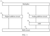
- an embodiment of this application provides a multiplier-adder (or referred to as a multiply and accumulate (multiply and accumulation, MAC)), including a multiplier 11, a digital addition circuit 12, an analog addition circuit 13, an analog-to-digital converter (analog-to-digital converter, ADC) 14, and a shift circuit 15.
- K is a positive integer.
- the multiplier 11 is configured to multiply a plurality of first values by a plurality of second values respectively to obtain a plurality of groups of partial products.
- the plurality of first values have a same quantity of bit positions, and the plurality of second values have a same quantity of bit positions.
- the multiplier 11 when compression encoding is not performed, may be a bit multiplication multiplier, for example, an AND gate, or may be a storage unit in a memory.
- the memory may be, for example, a static random access memory (static random access memory, SRAM), a register, a latch, an embedded flash (embedded flash, eFlash), a resistive random access memory (resistive random access memory, RRAM), or a phase change memory (phase change memory, PCM).
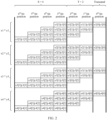
- a partial product in a group of partial products obtained by multiplying a first value by a second value, may be a value obtained by multiplying each bit in the first value by one bit in the second value, for example, x1[3]y1[0], x1[2]y1[0], x1[1]y1[0], or x1[0]y1[0] in FIG. 2 .
- a partial product may be a value obtained by multiplying each bit in the second value by one bit in the first value.
- the multiplier 11 may be a compression encoding multiplier, for example, a Booth (Booth) encoding multiplier or a canonic signed digit (canonic signed digit, CSD) encoding multiplier.
- a partial product in a group of partial products obtained by multiplying a first value by a second value, a partial product may be a value obtained by multiplying the first value by the second value through compression encoding, for example, one of -Y, 2Y, -2Y, and Y in FIG. 8 .
- a quantity of bit positions of the first value is E
- a quantity of bit positions of the second value is F
- a quantity of bit positions of a product value of a first value and a second value is E + F.
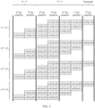
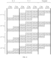
- the multiplier 11 is a bit multiplication multiplier. As shown in FIG. 2 to FIG. 4 , it is assumed that a plurality of first values are x1 to x4 respectively, a plurality of second values are y1 to y4 respectively, and the first value and the second value each occupy positions of four bits.
- the four bits of the first value x1 may be respectively represented as x1[0], x1[1], x1[2], and x1[3], and the four bits of the second value y1 may be respectively represented as y1[0], y1[1], y1[2], and y1[3], and so on.
- values that correspond to the 0 th bit positions of product values (referred to as product values for short below) of a first value and a second value and that are in a plurality of groups of partial products are x1[0]y1[0], x2[0]y2[0], x3[0]y3[0], and x4[0]y4[0] respectively.
- Values that correspond to the 1 st bit positions of the product values and that are in the plurality of groups of partial products are x1[1]y1[0], x1[0]y1[1], x2[1]y2[0], x2[0]y2[1], x3[1]y3[0], x3[0]y3[1], x4[1]y4[0], and x4[0]y4[1] respectively.
- Values that correspond to the 2 nd bit positions of the product values and that are in the plurality of groups of partial products are x1[2]y1[0], x1[1]y1[1], x1[0]y1[2], x2[2]y2[0], x2[1]y1[1], x2[0]y2[2], x3[2]y3[0], x3[1]y1[1], x3[0]y3[2], x4[2]y4[0], x4[1]y1[1], and x4[0]y4[2] respectively.
- values that correspond to the 6 th bit positions of the product values and that are in the plurality of groups of partial products are x1[3]y1[3], x2[3]y2[3], x3[3]y3[3] and x4[3]y4[3] respectively.
- the digital addition circuit 12 is configured to perform bitwise digital accumulation on bits that belong to a first bit position range and that are in the plurality of groups of partial products to obtain at least one (for example, S, where S is a positive integer) first summation value.
- a specific form of the digital addition circuit is not limited in this application.
- the digital addition circuit may be an adder tree structure in a circuit, for example, an array multiplier, a carry-save adder (carry-save adder, CSA), a carry-ripple adder (carry-ripple adder, CRA), a Wallace tree multiplier, or an approximate adder.
- the first bit position range refers to S bit positions of a product value of a first value and a second value.
- the first bit position range refers to S highest bit positions of a product value of a first value and a second value. Because precision of the digital addition circuit 12 is higher than precision of the analog addition circuit 13, using the digital addition circuit 12 to calculate a higher-position bit of a product value helps ensure that precision of the multiplier-adder is greater than a threshold.
- the digital addition circuit 12 may perform digital accumulation on eight partial products corresponding to the 5 th bit positions of the product values to obtain a first summation value.
- the digital addition circuit 12 may perform digital accumulation on four partial products corresponding to the 6 th bit positions of the product values to obtain a first summation value.
- a corresponding analog parameter when a bit position is 0 is different from a corresponding analog parameter when a bit position is 1.
- the analog addition circuit 13 is configured to perform bitwise analog accumulation on analog parameters corresponding to values of bits that belong to a second bit position range and that are in the plurality of groups of partial products to obtain at least one (for example, T, where T is a positive integer) summation analog parameter.
- the analog parameter may be a charge, a current, a voltage, time, a quantity of pulses, or the like. This is not limited in this application.
- the second bit position range refers to T bit positions that are of the product value and that do not overlap the first bit position range. S + T is less than or equal to a quantity of bit positions of the product value.
- Positions of the bits in the first bit position range are higher than positions of the bits in the second bit position range.
- the second bit position range refers to T bit positions that are lower than S bit positions and that are of a product value of a first value and a second value. Because power consumption of the analog addition circuit 13 is lower than power consumption of the digital addition circuit 12, using the analog addition circuit 13 to calculate a lower-position bit of a product value helps reduce power consumption of the multiplier-adder, to achieve a balance between precision and power consumption.
- T 2
- the analog addition circuit 13 may perform analog accumulation on analog parameters corresponding to eight partial products corresponding to the 1 st bit positions of the product values to obtain a summation analog parameter.
- the analog addition circuit 13 may perform analog accumulation on analog parameters corresponding to 12 partial products corresponding to the 2 nd bit positions of the product values to obtain a summation analog parameter.
- T 4.
- the analog addition circuit 13 may perform analog accumulation on analog parameters corresponding to eight partial products corresponding to the 1 st bit positions of the product values to obtain a summation analog parameter.
- the analog addition circuit 13 may perform analog accumulation on analog parameters corresponding to 12 partial products corresponding to the 2 nd bit positions of the product values to obtain a summation analog parameter.
- the analog addition circuit 13 may perform analog accumulation on analog parameters corresponding to 16 partial products corresponding to 3 rd bit positions of the product values to obtain a summation analog parameter.
- the analog addition circuit 13 may perform analog accumulation on analog parameters corresponding to 12 partial products corresponding to the 4 th bit positions of the product values to obtain a summation analog parameter.
- T 3.
- the analog addition circuit 13 may perform analog accumulation on analog parameters corresponding to 12 partial products corresponding to the 2 nd bit positions of the product values to obtain a summation analog parameter.
- the analog addition circuit 13 may perform analog accumulation on analog parameters corresponding to 16 partial products corresponding to 3 rd bit positions of the product values to obtain a summation analog parameter.
- the analog addition circuit 13 may perform analog accumulation on analog parameters corresponding to 12 partial products corresponding to the 4 th bit positions of the product values to obtain a summation analog parameter.
- the analog addition circuit 13 may further perform analog accumulation on analog parameters corresponding to values of first bit positions in the plurality of groups of partial products, multiply an accumulated analog parameter by a coefficient, and then a value obtained by accumulating analog parameters corresponding to values of second bit positions in the plurality of groups of partial products to obtain a summation analog parameter.
- the first bit positions and the second bit positions are adjacent bit positions in the second bit position range. In this way, a stage quantity of the analog-to-digital converter 14 can be fully utilized, to reduce power consumption of the multiplier-adder. For example, as shown in FIG.
- the analog addition circuit 13 may perform analog accumulation on analog parameters corresponding to the 4 th bit positions, multiply an accumulated analog parameter by a coefficient 2, and then add a value obtained by accumulating analog parameters corresponding to the 3 rd bit positions to obtain a summation analog parameter.
- the analog addition circuit 13 may perform analog accumulation on analog parameters corresponding to the 2 nd bit positions, multiply an accumulated analog parameter by a coefficient 2, and then add a value obtained by accumulating analog parameters corresponding to the 1 st bit positions to obtain a summation analog parameter.
- S + T may be less than or equal to a quantity of bit positions K of a product value of a first value and a second value, that is, S + T ⁇ K.
- (S + T) highest bit positions of the product value are valid bit positions (that is, finally reserved).
- Partial products corresponding to (K - (S + T)) lowest bit positions of the product value may not be calculated or may not be accumulated (that is, may be truncated), so that power consumption is further reduced.
- the 0 th bit positions of the product values of the first values and the second values are truncated.
- the 0 th bit positions and the 1 st bit positions of the product values of the first values and the second values are truncated.
- the analog-to-digital converter 14 is configured to perform analog-to-digital conversion on at least one summation analog parameter output by the analog addition circuit 13 to obtain at least one (for example, T) second summation value, so that the second summation value and the first summation value are unified as summation values in a digital form. Because T summation analog parameters are used for analog-to-digital conversion, the state quantity of the analog-to-digital converter 14 is 2 T .
- the shift circuit 15 is configured to perform shift on at least one first summation value and at least one second summation value, and then sum values obtained after the shift, to obtain target data.
- a quantity of bit positions of the target data is S + T. Because for all previously calculated summation values, bit positions at which the summation values are located in the target data are not considered, with reference to the bit positions at which the summation values are located in the target data, the summation values need to be shifted and then summed to obtain the target data. For example, it is assumed that a quantity of bit positions of the target data is 4, and four summation values are A, B, C, and D respectively. In this case, the finally obtained target data is 8 * A + 4 * B + 2 * C + D.
- the analog parameter is a current.
- the analog addition circuit 13 may accumulate partial products by accumulating currents corresponding to the partial products output by the multiplier 11.
- the multiplier 11 may include a plurality of word lines (word lines, WLs) (for example, WL 0 to WL 3), a plurality of bit lines (bit lines, BLs) (for example, BL 0 to BL 3), and a plurality of storage units (for example, an 8-transistor (transistor, 8T) storage unit in an SRAM) 111 in a memory.
- One word line may be coupled to the plurality of storage units 111 (for example, one row of storage units 111), and one bit line may also be coupled to the plurality of storage units 111 (for example, one column of storage units 111).
- the plurality of storage units 111 coupled to the word line are respectively configured to store one bit of a second value.
- a plurality of storage units 111 coupled to the word line WL 0 are respectively configured to store bits y1[0], y1[1], and y1[2] of a second value y1.
- One word line is configured to input bits of a first value in sequence in a time-division manner (in which a lower-position bit is first input and then a higher-position bit is input).
- the word line WL0 is configured to input bits x1[0], x 1 [1], and x 1 [2] of a first value x1 in a time-division manner.
- the plurality of storage units 111 coupled to the bit line are respectively configured to output, to the bit line, a current corresponding to one bit position in a partial product (that is, a partial product of multiplying one bit of the first value by one bit of the second value).
- a plurality of storage units 111 coupled to the bit line BL 2 are respectively configured to output, to the bit line BL 2, currents corresponding to the partial products x1[0] * y 1 [2], x2[0] * y2[2], x3[0] * y3[2], and x4[0] * y4[2].
- the analog addition circuit 13 includes a plurality of buffer circuits 131 (for example, C0 to C2) respectively coupled to the plurality of bit lines.
- a first buffer circuit 131 coupled to one bit line is configured to perform analog accumulation on the foregoing currents, and output an accumulated current to a second buffer circuit 131 coupled to another bit line.
- the second buffer circuit 131 not only performs analog accumulation on currents in the coupled bit line, but also accumulates charges from the first buffer circuit 131.
- the second buffer circuit 131 outputs a summation analog parameter to the ADC 14. For example, as shown in A in FIG.
- the buffer circuit C2 performs analog accumulation on the currents in the bit line BL 2, and outputs an accumulated current to the buffer circuit C1
- the buffer circuit C1 performs analog accumulation on currents in the bit line BL 1, and outputs an accumulated current to the buffer circuit C0.
- a summation analog parameter output by the buffer circuit C0 to the ADC 14 includes accumulation of the currents in the bit line BL 2, the bit line BL 1, and the bit line BL 0.
- the multiplier-adder may further include a plurality of first switches (for example, K0 to K2) respectively coupled to the plurality of bit lines.
- a first switch When a first switch is turned on, a bit line coupled to the first switch outputs a current to a buffer circuit 131 coupled to the bit line.
- the bit line coupled to the first switch When the first switch is turned off, the bit line coupled to the first switch does not output a current to the buffer circuit 131 coupled to the bit line. In this way, different summation analog parameters may be output by controlling the first switches to be turned on or off.
- the bit line BL 2 when the first switch K2, the first switch K1, and the first switch K0 are all turned on, the bit line BL 2, the bit line BL 1, and the bit line BL 0 may all output a current.
- y1[2], y2[2], y3[2], and y4[2] are respectively stored in a storage unit coupled to the word line BL 2.
- x1[0], x2[0], x3[0], and x4[0] are respectively input to the four word lines (WL 0 to WL 3).
- a summation analog parameter corresponding to a charge accumulated by the buffer circuit C2 coupled to the word line BL 2 is x1[0] * y1[2] + x2[0] * y2[2] + x3[0] * y3[2] + x4[0] * y4[2].
- y1[1], y2[1], y3[1], and y4[1] are respectively stored in a storage unit coupled to the word line BL 1.
- x1[1], x2[1], x3[1], and x4[1] are respectively input to the four word lines (WL 0 to WL 3), and a charge accumulated by the buffer circuit C2 is transferred to the buffer circuit C1.
- a summation analog parameter corresponding to the charge accumulated by the buffer circuit C1 is (x1[0] * y1[2]) + x2[0] * y2[2] + x3[0] * y3[2] + x4[0] * y4[2]) + (x1[1] * y1[1] + x2[1] * y2[1] + x3[1] * y3[1] + x4[1] * y4[1]).
- y1[0], y2[0], y3[0], and y4[0] are respectively stored in a storage unit coupled to the word line BL 0.
- x1[2], x2[2], x3[2], and x4[2] are respectively input to the four word lines (WL 0 to WL 3), and a charge accumulated by the buffer circuit C1 is transferred to the buffer circuit C0.
- a summation analog parameter corresponding to the charge accumulated by the buffer circuit C0 is (x1[0] * y1[2] + x2[0] * y2[2] + x3[0] * y3[2] + x4[0] * y4[2]) + (x1[1] * y1[1] + x2[1] * y2[1] + x3[1] * y3[1] + x4[1] * y4[1]) (x1[2] * y1[0] + x2[2] * y2[0] + x3[2] * y3[0] + x4[2] * y4[0]).
- This circuit structure may output the summation analog parameter of the 2 nd bit positions of the product values in FIG. 2 .
- the summation analog parameter corresponding to the charge accumulated by the buffer circuit C0 is output by the ADC 2, that is, a second summation value.
- the bit line BL 2 coupled to the first switch K2 does not output a current.
- y1[1], y2[1], y3[1], and y4[1] are respectively stored in a storage unit coupled to the word line BL 1.
- x1[0], x2[0], x3[0], and x4[0] are respectively input to the four word lines (WL 0 to WL 3).
- a summation analog parameter corresponding to a charge accumulated by the buffer circuit C1 is (x1[0] * y1[1] + x2[0] * y2[1] + x3[0] * y3 [1] + x4[0] * y4[1]).
- y1[0], y2[0], y3[0], and y4[0] are respectively stored in a storage unit coupled to the word line BL 0.
- x1[1], x2[1], x3[1], and x4[1] are respectively input to the four word lines (WL 0 to WL 3), and a charge accumulated by the buffer circuit C1 is transferred to the buffer circuit C0.
- a summation analog parameter corresponding to the charge accumulated by the buffer circuit C0 is (x1[0] * y1[1] + x2[0] * y2[1] + x3[0] * y3[1] + x4[0] * y4[1]) (x1[1] * y1[0] + x2[1] * y2[0] + x3[1] * y3[0] + x4[1] * y4[0]).
- This circuit structure may output the summation analog parameter of the 1 st bit positions of the product values in FIG. 2 .
- the summation analog parameter corresponding to the charge accumulated by the buffer circuit C0 is output by the ADC 2, that is, a second summation value.
- the analog parameter is a charge.
- the analog addition circuit 13 may accumulate partial products by accumulating charges corresponding to the partial products output by the multiplier 11.
- the multiplier 11 includes a plurality of groups of AND gates 112.
- the analog addition circuit 13 includes a plurality of capacitors 132 respectively coupled to output ends of the plurality of groups of AND gates 112, and a plurality of second switches 133 coupled to the plurality of capacitors 132. Capacitances of the plurality of capacitors 132 may be the same, so that a small capacitance may be used to improve precision.
- a capacitance of a capacitor coupled to an output end of an AND gate is set to being in a two-fold increasing relationship.
- a larger capacitance indicates poorer precision and a larger area, resulting in poor precision and an excessively large area of the multiplier-adder.
- a second AND gate implements x1[1] * y1[1].
- a third AND gate implements x1[0] * y1[2].
- this circuit structure may output the summation analog parameter of the 2 nd bit positions of the product values in FIG. 2 .
- this circuit structure may output the summation analog parameter of the 1 st bit positions of the product values in FIG. 2 .
- the multiplier 11 may further obtain the partial products by using various encoding circuits, for example, Booth (Booth) encoding circuit and canonic signed digit (canonic signed digit, CSD) encoding circuit.
- Booth Booth
- canonic signed digit canonic signed digit, CSD
- the Booth encoding may include Radix-4 (Radix-4) Booth encoding, Radix-8 (Radix-8) Booth encoding, and the like.
- the Radix-4 Booth encoding is used as an example. Every three bits of a value in a first value X or a second value Y may be used as a group of inputs of the multiplier 11, the other value is used as another input of the multiplier 11, and compression encoding is performed on the input values by the multiplier 11 to obtain a plurality of partial products.
- i is an integer
- a value of i in FIG. 7 may range from 0 to 3.
- the second value Y is used as another input of the multiplier 11. Compression encoding is performed on the input values by the multiplier 11 to obtain a plurality of partial products.
- a truth table of the multiplier 11 is shown in Table 1.
- a partial product Y indicates that the partial product is the same as the input Y
- a partial product 2Y indicates that all bit positions of the input Y are shifted leftward by one bit position.
- a partial product -Y indicates that a complement of the input Y is taken (that is, negation is performed on Y and 1 is added).
- a partial product -2Y indicates that all bit positions of the input Y are shifted leftward by one bit position and then a complement is taken.
- a partial product 0 indicates that each bit is 0.
- a first value X 100111
- a plurality of corresponding partial products, which are -Y, 2Y, -2Y, and Y respectively, may be obtained by querying Table 1.
- An embodiment of this application further provides a circuit optimization method, to generate and optimize the foregoing multiplier-adder, and may be applied to electronic design automation (electronic design automation, EDA). As shown in FIG. 9 , the method includes the following steps.
- S101 Obtain a first quantity of bit positions and a second quantity of bit positions.
- the first quantity of bit positions and the second quantity of bit positions each refer to a quantity of bit positions of a product value obtained by multiplying two values (for example, the first value and the second value described above).
- S102 Obtain a plurality of data pairs based on the first quantity of bit positions and the second quantity of bit positions.
- Precision of the multiplier-adder described above in each data pair is greater than a threshold.
- the data pair includes a first bit position range in which digital accumulation is performed by the multiplier-adder and a second bit position range in which analog accumulation is performed by the multiplier-adder.
- the first bit position range is less than or equal to a quantity of bit positions of the product value.
- step S102 may include the following step.
- S1021 Determine, based on a first quantity E of bit positions and a second quantity F of bit positions, that a quantity of bit positions of a product value of the two values output by the multiplier-adder is E + F.
- the first bit position range in which digital accumulation is performed is set to being equal to the quantity E + F of bit positions of the product value, and the precision of the multiplier-adder is calculated. Then, the first bit position range is gradually decreased and the precision of the multiplier-adder is calculated. If the precision of the multiplier-adder is greater than a first threshold, the first bit position range is added to the foregoing set, and the first bit position range is stopped being added to the set until the precision of the multiplier-adder is not greater than the first threshold.
- the set includes all candidate first bit position ranges.
- the first bit position range in which digital accumulation is performed refers to S highest bit positions of the product value of the two values.
- the precision of the multiplier-adder may be expressed by an error between multiplier-adders that completely use (that is, (E + F) bit positions) digital accumulation.
- S1023 Obtain a candidate second bit position range based on precision of the multiplier-adder in the candidate first bit position range and different second bit position ranges.
- a candidate first bit position range is selected from the set. Precision of the multiplier-adder in the candidate first bit position range and the different second bit position ranges is calculated. The candidate second bit position range (the smallest second bit position range when the precision is greater than a second threshold) and the candidate first bit position range are added to a data pair. Minimum precision of the multiplier-adder in the candidate first bit position range is less than minimum precision of the multiplier-adder in the candidate first bit position range and the different second bit position ranges.
- a second bit position range T on which analog accumulation is performed is set to E + F - S. Then the second bit position range T on which analog accumulation is performed is gradually decreased, and precision of the multiplier-adder is calculated until the precision of the multiplier-adder is not greater than the second threshold (where the second threshold is greater than the first threshold). In this way, the minimum second bit position range in which analog accumulation is performed may be determined.
- S103 Calculate power consumption of the multiplier-adder in each data pair, and determine an optimal data pair from the data pairs.
- the power consumption of the multiplier-adder mainly includes power consumption of a digital addition circuit (which is affected by the first bit position range in which digital accumulation is performed), power consumption of an analog addition circuit (which is affected by a quantity T of bit positions on which analog accumulation is performed), and power consumption of an ADC (which is affected by a quantity of bit positions of a digital parameter output by the ADC).
- the power consumption of the ADC is not in a linear relationship with the quantity of bit positions of the digital parameter output by the ADC.
- power consumption of an ADC of which output digital parameter is 5 bits is only 20% higher than power consumption of an ADC of which output digital parameter is 4 bits.
- power consumption of an ADC of which output digital parameter is 12 bits is many times higher than power consumption of an ADC of which output digital parameter is 11 bits.
- the multiplier-adder described above may be generated, and the multiplier-adder mainly affects a quantity of bit positions of the digital addition circuit and a quantity of bit positions of the analog addition circuit.
- the multiplier-adder in this application may be used in an architecture in which multiplication and accumulation are implemented based on in-memory computing or near-memory computing of a storage unit.
- the storage unit may be a storage unit in a memory such as a static random access memory (static random access memory, SRAM), a register, a latch, an embedded flash (embedded flash, eFlash), a resistive random access memory (resistive random access memory, RRAM), or a phase change memory (phase change memory, PCM).
- the multiplier-adder may be used in a scenario in which the second value does not change frequently but the first value changes frequently, for example, a flow processing acceleration chip or a neural network acceleration chip.
- the multiplier-adder may be further used in a scenario in which both the second value and the first value change frequently, for example, a signal processing chip in the communications field or a low-delay multiply-add kernel in a neural network chip.
- the bitwise digital accumulation is performed, by using the digital addition circuit, on the bits that belong to the first bit position range and that are in the plurality of groups of partial products.
- the bitwise analog accumulation is performed, by using the analog addition circuit, on the analog parameters corresponding to the values of the bits that belong to the second bit position range and that are in the plurality of groups of partial products.
- the first bit position range refers to the S bit positions of the product value of one of the first values and one of the second values.
- the second bit position range refers to the T bit positions that are of the product value and that do not overlap the first bit position range.
- An embodiment of this application further provides a computer-readable storage medium, storing instructions.
- the instructions When the instructions are executed on a computer, the computer is enabled to perform the methods in FIG. 9 and FIG. 10 .
- An embodiment of this application further provides a computer program product including instructions.
- the instructions When the instructions are executed on a computer, the computer is enabled to perform the methods in FIG. 9 and FIG. 10 .
- sequence numbers of the foregoing processes do not mean execution sequences in various embodiments of this application.
- the execution sequences of the processes should be determined according to functions and internal logic of the processes, and should not be construed as any limitation on the implementation processes of embodiments of this application.
- modules and algorithm steps may be implemented by electronic hardware or a combination of computer software and electronic hardware. Whether the functions are performed by hardware or software depends on particular applications and design constraint conditions of the technical solutions. A person skilled in the art may use different methods to implement the described functions for each particular application, but it should not be considered that the implementation goes beyond the scope of this application.
- the disclosed system, device, and method may be implemented in other manners.
- the described device embodiment is merely an example.
- division into the modules is merely logical function division and may be other division in an actual implementation.
- a plurality of modules or components may be combined or integrated into another device, or some features may be ignored or not performed.
- the displayed or discussed mutual couplings or direct couplings or communication connections may be implemented through some interfaces.
- the indirect couplings or communication connections between the devices or modules may be implemented in electronic, mechanical, or other forms.
- modules described as separate components may or may not be physically separate, and components displayed as modules may or may not be physical modules, may be located in one device, or may be distributed on a plurality of devices. Some or all the modules may be selected according to actual needs to achieve the objectives of the solutions of embodiments.
- modules in embodiments of this application may be integrated into one device, or each of the modules may exist alone physically, or two or more modules are integrated into one device.
- All or some of the foregoing embodiments may be implemented by using software, hardware, firmware, or any combination thereof.
- a software program is used to implement embodiments, all or some of embodiments may be implemented in a form of a computer program product.
- the computer program product includes one or more computer instructions. When the computer program instructions are loaded and executed on a computer, all or some of the procedure or functions according to embodiments of this application are generated.
- the computer may be a general-purpose computer, a dedicated computer, a computer network, or another programmable apparatus.
- the computer instructions may be stored in a computer-readable storage medium or may be transmitted from a computer-readable storage medium to another computer-readable storage medium.
- the computer instructions may be transmitted from a website, computer, server, or data center to another website, computer, server, or data center in a wired (for example, a coaxial cable, an optical fiber, or a digital subscriber line (Digital Subscriber Line, DSL)) or wireless (for example, infrared, radio, or microwave) manner.
- the computer-readable storage medium may be any usable medium accessible by the computer, or a data storage device, such as a server or a data center, integrating one or more usable media.
- the usable medium may be a magnetic medium (for example, a floppy disk, a hard disk, or a magnetic tape), an optical medium (for example, a DVD), a semiconductor medium (for example, a solid-state drive (Solid-State Drive, SSD)), or the like.
- a magnetic medium for example, a floppy disk, a hard disk, or a magnetic tape
- an optical medium for example, a DVD
- a semiconductor medium for example, a solid-state drive (Solid-State Drive, SSD)
Landscapes
- Engineering & Computer Science (AREA)
- Physics & Mathematics (AREA)
- General Physics & Mathematics (AREA)
- Theoretical Computer Science (AREA)
- Computational Mathematics (AREA)
- Computing Systems (AREA)
- Mathematical Analysis (AREA)
- Mathematical Optimization (AREA)
- Pure & Applied Mathematics (AREA)
- General Engineering & Computer Science (AREA)
- Analogue/Digital Conversion (AREA)
Applications Claiming Priority (2)
| Application Number | Priority Date | Filing Date | Title |
|---|---|---|---|
| CN202111676335.1A CN116414352A (zh) | 2021-12-31 | 2021-12-31 | 电路、乘加器和电路优化方法 |
| PCT/CN2022/130963 WO2023124561A1 (fr) | 2021-12-31 | 2022-11-09 | Circuit, multiplicateur et procédé d'optimisation de circuit |
Publications (3)
| Publication Number | Publication Date |
|---|---|
| EP4432074A1 true EP4432074A1 (fr) | 2024-09-18 |
| EP4432074A4 EP4432074A4 (fr) | 2025-03-12 |
| EP4432074B1 EP4432074B1 (fr) | 2026-02-25 |
Family
ID=86997589
Family Applications (1)
| Application Number | Title | Priority Date | Filing Date |
|---|---|---|---|
| EP22913824.3A Active EP4432074B1 (fr) | 2021-12-31 | 2022-11-09 | Circuit, multiplicateur et procédé d'optimisation de circuit |
Country Status (4)
| Country | Link |
|---|---|
| US (1) | US20240355372A1 (fr) |
| EP (1) | EP4432074B1 (fr) |
| CN (1) | CN116414352A (fr) |
| WO (1) | WO2023124561A1 (fr) |
Family Cites Families (7)
| Publication number | Priority date | Publication date | Assignee | Title |
|---|---|---|---|---|
| US4831577A (en) * | 1986-09-17 | 1989-05-16 | Intersil, Inc. | Digital multiplier architecture with triple array summation of partial products |
| US6535901B1 (en) * | 2000-04-26 | 2003-03-18 | Sigmatel, Inc. | Method and apparatus for generating a fast multiply accumulator |
| US7136893B2 (en) * | 2003-07-10 | 2006-11-14 | International Business Machines Corporation | Decimal multiplication using digit recoding |
| CN105808206B (zh) * | 2016-03-04 | 2019-01-08 | 广州海格通信集团股份有限公司 | 基于ram实现乘法运算的方法及其系统 |
| US10402168B2 (en) * | 2016-10-01 | 2019-09-03 | Intel Corporation | Low energy consumption mantissa multiplication for floating point multiply-add operations |
| KR102863235B1 (ko) * | 2019-09-17 | 2025-09-24 | 아나플래시 인코포레이티드 | 곱셈-누산 유닛 |
| US12462150B2 (en) * | 2021-10-31 | 2025-11-04 | Ceremorphic, Inc. | Modular analog multiplier-accumulator unit element for multi-layer neural networks |
-
2021
- 2021-12-31 CN CN202111676335.1A patent/CN116414352A/zh active Pending
-
2022
- 2022-11-09 EP EP22913824.3A patent/EP4432074B1/fr active Active
- 2022-11-09 WO PCT/CN2022/130963 patent/WO2023124561A1/fr not_active Ceased
-
2024
- 2024-06-28 US US18/759,492 patent/US20240355372A1/en active Pending
Also Published As
| Publication number | Publication date |
|---|---|
| EP4432074A4 (fr) | 2025-03-12 |
| US20240355372A1 (en) | 2024-10-24 |
| CN116414352A (zh) | 2023-07-11 |
| EP4432074B1 (fr) | 2026-02-25 |
| WO2023124561A1 (fr) | 2023-07-06 |
Similar Documents
| Publication | Publication Date | Title |
|---|---|---|
| TWI701612B (zh) | 用於神經網路中激勵函數的電路系統及其處理方法 | |
| You et al. | A 1–8b reconfigurable digital sram compute-in-memory macro for processing neural networks | |
| Jia et al. | A microprocessor implemented in 65nm CMOS with configurable and bit-scalable accelerator for programmable in-memory computing | |
| WO2020029018A1 (fr) | Procédé et appareil de traitement de matrice, et circuit logique | |
| Jeong et al. | A ternary neural network computing-in-memory processor with 16T1C bitcell architecture | |
| US10877733B2 (en) | Segment divider, segment division operation method, and electronic device | |
| US9983850B2 (en) | Shared hardware integer/floating point divider and square root logic unit and associated methods | |
| CN111381808A (zh) | 乘法器、数据处理方法、芯片及电子设备 | |
| Zhang et al. | In-memory multibit multiplication based on bitline shifting | |
| EP4432074B1 (fr) | Circuit, multiplicateur et procédé d'optimisation de circuit | |
| CN110941185A (zh) | 一种用于二值神经网络的双字线6tsram单元电路 | |
| CN115220690A (zh) | 存储器装置及其操作方法 | |
| US11435981B2 (en) | Arithmetic circuit, and neural processing unit and electronic apparatus including the same | |
| JP7820400B2 (ja) | 再構成可能なアナログベースのニューラルネットワークにおけるマルチビットmacアレイのためのアナログ加算器 | |
| CN118036682A (zh) | 加法神经网络的存内计算实现方法、装置、设备及介质 | |
| US11764801B2 (en) | Computing-in-memory circuit | |
| CN110515586B (zh) | 乘法器、数据处理方法、芯片及电子设备 | |
| Kuo et al. | A lower error antilogarithmic converter using novel four-region piecewise-linear approximation | |
| CN110378477B (zh) | 乘法器、数据处理方法、芯片及电子设备 | |
| US20160142042A1 (en) | Elimination method for common sub-expression | |
| KR102878901B1 (ko) | 삼진 뉴럴 네트워크 연산 가속을 위한 컴퓨팅 인 메모리 장치 | |
| US10732931B2 (en) | Negative operand compatible charge-scaling subtractor circuit | |
| CN209895329U (zh) | 乘法器 | |
| Patel et al. | Modified error tolerant adder for digital signal processing applictaion | |
| CN115658730B (zh) | 稀疏数据的查询方法、装置、设备和计算机可读存储介质 |
Legal Events
| Date | Code | Title | Description |
|---|---|---|---|
| STAA | Information on the status of an ep patent application or granted ep patent |
Free format text: STATUS: THE INTERNATIONAL PUBLICATION HAS BEEN MADE |
|
| PUAI | Public reference made under article 153(3) epc to a published international application that has entered the european phase |
Free format text: ORIGINAL CODE: 0009012 |
|
| STAA | Information on the status of an ep patent application or granted ep patent |
Free format text: STATUS: REQUEST FOR EXAMINATION WAS MADE |
|
| 17P | Request for examination filed |
Effective date: 20240612 |
|
| AK | Designated contracting states |
Kind code of ref document: A1 Designated state(s): AL AT BE BG CH CY CZ DE DK EE ES FI FR GB GR HR HU IE IS IT LI LT LU LV MC ME MK MT NL NO PL PT RO RS SE SI SK SM TR |
|
| A4 | Supplementary search report drawn up and despatched |
Effective date: 20250211 |
|
| RIC1 | Information provided on ipc code assigned before grant |
Ipc: G06F 7/544 20060101AFI20250205BHEP |
|
| DAV | Request for validation of the european patent (deleted) | ||
| DAX | Request for extension of the european patent (deleted) | ||
| GRAP | Despatch of communication of intention to grant a patent |
Free format text: ORIGINAL CODE: EPIDOSNIGR1 |
|
| STAA | Information on the status of an ep patent application or granted ep patent |
Free format text: STATUS: GRANT OF PATENT IS INTENDED |
|
| INTG | Intention to grant announced |
Effective date: 20251016 |
|
| GRAS | Grant fee paid |
Free format text: ORIGINAL CODE: EPIDOSNIGR3 |
|
| GRAA | (expected) grant |
Free format text: ORIGINAL CODE: 0009210 |
|
| STAA | Information on the status of an ep patent application or granted ep patent |
Free format text: STATUS: THE PATENT HAS BEEN GRANTED |
|
| AK | Designated contracting states |
Kind code of ref document: B1 Designated state(s): AL AT BE BG CH CY CZ DE DK EE ES FI FR GB GR HR HU IE IS IT LI LT LU LV MC ME MK MT NL NO PL PT RO RS SE SI SK SM TR |
|
| REG | Reference to a national code |
Ref country code: CH Ref legal event code: F10 Free format text: ST27 STATUS EVENT CODE: U-0-0-F10-F00 (AS PROVIDED BY THE NATIONAL OFFICE) Effective date: 20260225 Ref country code: GB Ref legal event code: FG4D |
|
| REG | Reference to a national code |
Ref country code: DE Ref legal event code: R096 Ref document number: 602022031380 Country of ref document: DE |
|
| REG | Reference to a national code |
Ref country code: IE Ref legal event code: FG4D |