EP4435502A1 - Elektrooptischer modulator - Google Patents
Elektrooptischer modulator Download PDFInfo
- Publication number
- EP4435502A1 EP4435502A1 EP23759017.9A EP23759017A EP4435502A1 EP 4435502 A1 EP4435502 A1 EP 4435502A1 EP 23759017 A EP23759017 A EP 23759017A EP 4435502 A1 EP4435502 A1 EP 4435502A1
- Authority
- EP
- European Patent Office
- Prior art keywords
- electrode
- layer
- waveguide
- extension
- electro
- Prior art date
- Legal status (The legal status is an assumption and is not a legal conclusion. Google has not performed a legal analysis and makes no representation as to the accuracy of the status listed.)
- Pending
Links
Images


Classifications
-
- G—PHYSICS
- G02—OPTICS
- G02F—OPTICAL DEVICES OR ARRANGEMENTS FOR THE CONTROL OF LIGHT BY MODIFICATION OF THE OPTICAL PROPERTIES OF THE MEDIA OF THE ELEMENTS INVOLVED THEREIN; NON-LINEAR OPTICS; FREQUENCY-CHANGING OF LIGHT; OPTICAL LOGIC ELEMENTS; OPTICAL ANALOGUE/DIGITAL CONVERTERS
- G02F1/00—Devices or arrangements for the control of the intensity, colour, phase, polarisation or direction of light arriving from an independent light source, e.g. switching, gating or modulating; Non-linear optics
- G02F1/01—Devices or arrangements for the control of the intensity, colour, phase, polarisation or direction of light arriving from an independent light source, e.g. switching, gating or modulating; Non-linear optics for the control of the intensity, phase, polarisation or colour
- G02F1/03—Devices or arrangements for the control of the intensity, colour, phase, polarisation or direction of light arriving from an independent light source, e.g. switching, gating or modulating; Non-linear optics for the control of the intensity, phase, polarisation or colour based on ceramics or electro-optical crystals, e.g. exhibiting Pockels effect or Kerr effect
- G02F1/035—Devices or arrangements for the control of the intensity, colour, phase, polarisation or direction of light arriving from an independent light source, e.g. switching, gating or modulating; Non-linear optics for the control of the intensity, phase, polarisation or colour based on ceramics or electro-optical crystals, e.g. exhibiting Pockels effect or Kerr effect in an optical waveguide structure
-
- G—PHYSICS
- G02—OPTICS
- G02F—OPTICAL DEVICES OR ARRANGEMENTS FOR THE CONTROL OF LIGHT BY MODIFICATION OF THE OPTICAL PROPERTIES OF THE MEDIA OF THE ELEMENTS INVOLVED THEREIN; NON-LINEAR OPTICS; FREQUENCY-CHANGING OF LIGHT; OPTICAL LOGIC ELEMENTS; OPTICAL ANALOGUE/DIGITAL CONVERTERS
- G02F1/00—Devices or arrangements for the control of the intensity, colour, phase, polarisation or direction of light arriving from an independent light source, e.g. switching, gating or modulating; Non-linear optics
- G02F1/01—Devices or arrangements for the control of the intensity, colour, phase, polarisation or direction of light arriving from an independent light source, e.g. switching, gating or modulating; Non-linear optics for the control of the intensity, phase, polarisation or colour
- G02F1/21—Devices or arrangements for the control of the intensity, colour, phase, polarisation or direction of light arriving from an independent light source, e.g. switching, gating or modulating; Non-linear optics for the control of the intensity, phase, polarisation or colour by interference
- G02F1/225—Devices or arrangements for the control of the intensity, colour, phase, polarisation or direction of light arriving from an independent light source, e.g. switching, gating or modulating; Non-linear optics for the control of the intensity, phase, polarisation or colour by interference in an optical waveguide structure
- G02F1/2255—Devices or arrangements for the control of the intensity, colour, phase, polarisation or direction of light arriving from an independent light source, e.g. switching, gating or modulating; Non-linear optics for the control of the intensity, phase, polarisation or colour by interference in an optical waveguide structure controlled by a high-frequency electromagnetic component in an electric waveguide structure
-
- G—PHYSICS
- G02—OPTICS
- G02F—OPTICAL DEVICES OR ARRANGEMENTS FOR THE CONTROL OF LIGHT BY MODIFICATION OF THE OPTICAL PROPERTIES OF THE MEDIA OF THE ELEMENTS INVOLVED THEREIN; NON-LINEAR OPTICS; FREQUENCY-CHANGING OF LIGHT; OPTICAL LOGIC ELEMENTS; OPTICAL ANALOGUE/DIGITAL CONVERTERS
- G02F1/00—Devices or arrangements for the control of the intensity, colour, phase, polarisation or direction of light arriving from an independent light source, e.g. switching, gating or modulating; Non-linear optics
- G02F1/01—Devices or arrangements for the control of the intensity, colour, phase, polarisation or direction of light arriving from an independent light source, e.g. switching, gating or modulating; Non-linear optics for the control of the intensity, phase, polarisation or colour
- G02F1/03—Devices or arrangements for the control of the intensity, colour, phase, polarisation or direction of light arriving from an independent light source, e.g. switching, gating or modulating; Non-linear optics for the control of the intensity, phase, polarisation or colour based on ceramics or electro-optical crystals, e.g. exhibiting Pockels effect or Kerr effect
-
- G—PHYSICS
- G02—OPTICS
- G02F—OPTICAL DEVICES OR ARRANGEMENTS FOR THE CONTROL OF LIGHT BY MODIFICATION OF THE OPTICAL PROPERTIES OF THE MEDIA OF THE ELEMENTS INVOLVED THEREIN; NON-LINEAR OPTICS; FREQUENCY-CHANGING OF LIGHT; OPTICAL LOGIC ELEMENTS; OPTICAL ANALOGUE/DIGITAL CONVERTERS
- G02F1/00—Devices or arrangements for the control of the intensity, colour, phase, polarisation or direction of light arriving from an independent light source, e.g. switching, gating or modulating; Non-linear optics
- G02F1/01—Devices or arrangements for the control of the intensity, colour, phase, polarisation or direction of light arriving from an independent light source, e.g. switching, gating or modulating; Non-linear optics for the control of the intensity, phase, polarisation or colour
- G02F1/03—Devices or arrangements for the control of the intensity, colour, phase, polarisation or direction of light arriving from an independent light source, e.g. switching, gating or modulating; Non-linear optics for the control of the intensity, phase, polarisation or colour based on ceramics or electro-optical crystals, e.g. exhibiting Pockels effect or Kerr effect
- G02F1/0305—Constructional arrangements
- G02F1/0316—Electrodes
-
- G—PHYSICS
- G02—OPTICS
- G02F—OPTICAL DEVICES OR ARRANGEMENTS FOR THE CONTROL OF LIGHT BY MODIFICATION OF THE OPTICAL PROPERTIES OF THE MEDIA OF THE ELEMENTS INVOLVED THEREIN; NON-LINEAR OPTICS; FREQUENCY-CHANGING OF LIGHT; OPTICAL LOGIC ELEMENTS; OPTICAL ANALOGUE/DIGITAL CONVERTERS
- G02F1/00—Devices or arrangements for the control of the intensity, colour, phase, polarisation or direction of light arriving from an independent light source, e.g. switching, gating or modulating; Non-linear optics
- G02F1/01—Devices or arrangements for the control of the intensity, colour, phase, polarisation or direction of light arriving from an independent light source, e.g. switching, gating or modulating; Non-linear optics for the control of the intensity, phase, polarisation or colour
- G02F1/03—Devices or arrangements for the control of the intensity, colour, phase, polarisation or direction of light arriving from an independent light source, e.g. switching, gating or modulating; Non-linear optics for the control of the intensity, phase, polarisation or colour based on ceramics or electro-optical crystals, e.g. exhibiting Pockels effect or Kerr effect
- G02F1/035—Devices or arrangements for the control of the intensity, colour, phase, polarisation or direction of light arriving from an independent light source, e.g. switching, gating or modulating; Non-linear optics for the control of the intensity, phase, polarisation or colour based on ceramics or electro-optical crystals, e.g. exhibiting Pockels effect or Kerr effect in an optical waveguide structure
- G02F1/0356—Devices or arrangements for the control of the intensity, colour, phase, polarisation or direction of light arriving from an independent light source, e.g. switching, gating or modulating; Non-linear optics for the control of the intensity, phase, polarisation or colour based on ceramics or electro-optical crystals, e.g. exhibiting Pockels effect or Kerr effect in an optical waveguide structure controlled by a high-frequency electromagnetic wave component in an electric waveguide structure
-
- G—PHYSICS
- G02—OPTICS
- G02F—OPTICAL DEVICES OR ARRANGEMENTS FOR THE CONTROL OF LIGHT BY MODIFICATION OF THE OPTICAL PROPERTIES OF THE MEDIA OF THE ELEMENTS INVOLVED THEREIN; NON-LINEAR OPTICS; FREQUENCY-CHANGING OF LIGHT; OPTICAL LOGIC ELEMENTS; OPTICAL ANALOGUE/DIGITAL CONVERTERS
- G02F1/00—Devices or arrangements for the control of the intensity, colour, phase, polarisation or direction of light arriving from an independent light source, e.g. switching, gating or modulating; Non-linear optics
- G02F1/01—Devices or arrangements for the control of the intensity, colour, phase, polarisation or direction of light arriving from an independent light source, e.g. switching, gating or modulating; Non-linear optics for the control of the intensity, phase, polarisation or colour
- G02F1/21—Devices or arrangements for the control of the intensity, colour, phase, polarisation or direction of light arriving from an independent light source, e.g. switching, gating or modulating; Non-linear optics for the control of the intensity, phase, polarisation or colour by interference
- G02F1/212—Mach-Zehnder type
-
- G—PHYSICS
- G02—OPTICS
- G02F—OPTICAL DEVICES OR ARRANGEMENTS FOR THE CONTROL OF LIGHT BY MODIFICATION OF THE OPTICAL PROPERTIES OF THE MEDIA OF THE ELEMENTS INVOLVED THEREIN; NON-LINEAR OPTICS; FREQUENCY-CHANGING OF LIGHT; OPTICAL LOGIC ELEMENTS; OPTICAL ANALOGUE/DIGITAL CONVERTERS
- G02F1/00—Devices or arrangements for the control of the intensity, colour, phase, polarisation or direction of light arriving from an independent light source, e.g. switching, gating or modulating; Non-linear optics
- G02F1/01—Devices or arrangements for the control of the intensity, colour, phase, polarisation or direction of light arriving from an independent light source, e.g. switching, gating or modulating; Non-linear optics for the control of the intensity, phase, polarisation or colour
- G02F1/21—Devices or arrangements for the control of the intensity, colour, phase, polarisation or direction of light arriving from an independent light source, e.g. switching, gating or modulating; Non-linear optics for the control of the intensity, phase, polarisation or colour by interference
- G02F1/225—Devices or arrangements for the control of the intensity, colour, phase, polarisation or direction of light arriving from an independent light source, e.g. switching, gating or modulating; Non-linear optics for the control of the intensity, phase, polarisation or colour by interference in an optical waveguide structure
-
- G—PHYSICS
- G02—OPTICS
- G02F—OPTICAL DEVICES OR ARRANGEMENTS FOR THE CONTROL OF LIGHT BY MODIFICATION OF THE OPTICAL PROPERTIES OF THE MEDIA OF THE ELEMENTS INVOLVED THEREIN; NON-LINEAR OPTICS; FREQUENCY-CHANGING OF LIGHT; OPTICAL LOGIC ELEMENTS; OPTICAL ANALOGUE/DIGITAL CONVERTERS
- G02F1/00—Devices or arrangements for the control of the intensity, colour, phase, polarisation or direction of light arriving from an independent light source, e.g. switching, gating or modulating; Non-linear optics
- G02F1/01—Devices or arrangements for the control of the intensity, colour, phase, polarisation or direction of light arriving from an independent light source, e.g. switching, gating or modulating; Non-linear optics for the control of the intensity, phase, polarisation or colour
- G02F1/21—Devices or arrangements for the control of the intensity, colour, phase, polarisation or direction of light arriving from an independent light source, e.g. switching, gating or modulating; Non-linear optics for the control of the intensity, phase, polarisation or colour by interference
- G02F1/225—Devices or arrangements for the control of the intensity, colour, phase, polarisation or direction of light arriving from an independent light source, e.g. switching, gating or modulating; Non-linear optics for the control of the intensity, phase, polarisation or colour by interference in an optical waveguide structure
- G02F1/2257—Devices or arrangements for the control of the intensity, colour, phase, polarisation or direction of light arriving from an independent light source, e.g. switching, gating or modulating; Non-linear optics for the control of the intensity, phase, polarisation or colour by interference in an optical waveguide structure the optical waveguides being made of semiconducting material
Definitions
- the present disclosure relates to the technical field of optical communications, and in particular, to an electro-optic modulator.
- Optical communications have achieved rapid development in the direction of high-speed and large-capacity communications due to their characteristics such as a large bandwidth, high reliability, a low cost and a strong anti-interference ability. How to load high-speed electrical signals onto optical carriers is a core research content.
- An electro-optic modulator is a modulator that is made based on an electro-optic effect of electro-optic materials.
- the electro-optic effect means that when a voltage is applied to an electro-optic material such as a lithium niobate crystal, a gallium arsenide crystal, or a lithium tantalate crystal, a refractive index of the electro-optic material will vary, resulting in a change in characteristics of light waves passing through the electro-optic material.
- the use of the electro-optic effect allows modulation of parameters, such as the phase, amplitude, intensity and polarization state, of optical signals.
- An embodiment of the present disclosure provides an electro-optic modulator, including: a light splitting element; a light combining element; a first waveguide arm and a second waveguide arm that are arranged in parallel and are connected between the light splitting element and the light combining element; and a first ground electrode, a first signal electrode, a second ground electrode, a second signal electrode, and a third ground electrode that are arranged in sequence, where the first signal electrode and the second signal electrode are configured to receive differential signals, the first waveguide arm is located between the first ground electrode and the first signal electrode, and the second waveguide arm is located between the second ground electrode and the second signal electrode.
- the electro-optic modulator further includes: a first independent waveguide section and a second independent waveguide section that are arranged in parallel with the first waveguide arm and the second waveguide arm, where the first independent waveguide section is located between the first signal electrode and the second ground electrode, and the second independent waveguide section is located between the second signal electrode and the third ground electrode.
- the electro-optic modulator includes a substrate, an isolation layer, a waveguide layer, and an electrode layer that are arranged in sequence, where the first waveguide arm and the second waveguide arm are located in the waveguide layer; and the first ground electrode, the first signal electrode, the second ground electrode, the second signal electrode, and the third ground electrode are located in the electrode layer.
- the first signal electrode and the second signal electrode each include a first main electrode with a distance of h1 from the substrate, and the first ground electrode, the second ground electrode, and the third ground electrode each include a second main electrode with a distance of h2 from the substrate, where h1 ⁇ h2.
- the electro-optic modulator further includes a dielectric layer located between the waveguide layer and the electrode layer, and a dielectric constant of the dielectric layer is less than that of the waveguide layer, where the waveguide layer includes a flat plate layer and a ridged layer located at a side of the flat plate layer away from the substrate, the first waveguide arm and the second waveguide arm are located in the ridged layer, the first main electrode is formed on a surface of a side of the dielectric layer away from the substrate, and the second main electrode is formed on a surface of a side of the flat plate layer away from the substrate.
- the electro-optic modulator further includes a dielectric layer located between the waveguide layer and the electrode layer, and a dielectric constant of the dielectric layer is less than that of the waveguide layer, where the waveguide layer is a ridged pattern layer, the first main electrode is formed on a surface of a side of the dielectric layer away from the substrate, and the second main electrode is formed on a surface of a side of the isolation layer away from the substrate.
- each of the first signal electrode and the second signal electrode further includes a first extension electrode correspondingly connected to the respective first main electrode.
- each of the first ground electrode, the second ground electrode, and the third ground electrode further includes a second extension electrode correspondingly connected to the respective second main electrode.
- each of the first signal electrode and the second signal electrode further includes a first extension electrode correspondingly connected to the respective first main electrode, where the first extension electrode is a surface-shaped extension electrode with the same extension direction as the first main electrode, or the first extension electrode includes a plurality of first sub-electrodes arranged at intervals in the extension direction of the first main electrode; and each of the first ground electrode, the second ground electrode, and the third ground electrode further includes a second extension electrode correspondingly connected to the respective second main electrode, where the second extension electrode is a surface-shaped extension electrode with the same extension direction as the second main electrode, or the second extension electrode includes a plurality of second sub-electrodes arranged at intervals in the extension direction of the second main electrode, where at least a part of the first extension electrode and at least a part of the second extension electrode are located in the same plane.
- the waveguide layer includes a flat plate layer and a ridged layer located at a side of the flat plate layer away from the substrate, the first waveguide arm and the second waveguide arm are located in the ridged layer, and at least a part of the first extension electrode and at least a part of the second extension electrode are formed on a surface of a side of the flat plate layer away from the substrate.
- the waveguide layer is a ridged pattern layer, and at least a part of the first extension electrode and at least a part of the second extension electrode are formed on a surface of a side of the isolation layer away from the substrate.
- the first ground electrode includes one second extension electrode, which is arranged at a side of the first ground electrode close to the first signal electrode;
- the first signal electrode includes two first extension electrodes, which are distributed at two sides of the first signal electrode;
- the second ground electrode includes two second extension electrodes, which are distributed at two sides of the second ground electrode;
- the second signal electrode includes two first extension electrodes, which are distributed at two sides of the second signal electrode;
- the third ground electrode includes one second extension electrode, which is arranged at a side of the third ground electrode close to the second signal electrode.
- the waveguide layer includes a flat plate layer and a ridged layer located at a side of the flat plate layer away from the substrate, where the first waveguide arm and the second waveguide arm are located in the ridged layer, and the first main electrode or the second main electrode penetrates the flat plate layer and is in contact with the isolation layer.
- the electro-optic modulator further includes a dielectric layer located between the waveguide layer and the electrode layer, where a dielectric constant of the dielectric layer is less than that of the waveguide layer, and the dielectric layer covers the first waveguide arm and the second waveguide arm.
- a Mach-Zehnder modulator is one type of electro-optic modulator, in which an input optical signal is equally split into two branch optical signals, which then enter two waveguide arms, respectively.
- the two waveguide arms are made of an electro-optic material and have a refractive index changing with an applied modulation voltage.
- the change in the refractive index of the waveguide arms may lead to a change in phases of the branch optical signals. Therefore, an output from the convergence of the two branch optical signals is an interference signal with an intensity changing with the modulation voltage.
- the Mach-Zehnder modulator can implement modulation of different sidebands by controlling the modulation voltage applied to the two waveguide arms.
- the Mach-Zehnder modulator is one of the common core devices in optical interconnection, optical computing and optical communication systems.
- FIG. 1 which shows a schematic structural diagram of a conventional Mach-Zehnder modulator.
- the Mach-Zehnder modulator 001 has two waveguide arms 02 that are strictly identical to each other.
- the Mach-Zehnder modulator 001 is not working, neither of the two waveguide arms 02 undergoes an electro-optic effect.
- Input light passes through a light splitting element 01 and is then equally split into two branch optical signals.
- the two branch optical signals are still in the same phase after respectively passing through the corresponding waveguide arms 02, and then a coherently enhanced signal for the two branch optical signals will be output from a light combining element 05.
- a modulating electrode 04 (for example, including a signal electrode 040, a first ground electrode 041, and a second ground electrode 042) applies a modulation voltage to the two waveguide arms 02, and the two branch optical signals may differ in phase by an odd or even multiple of ⁇ after each of the two branch optical signals passes through one waveguide arm 02.
- the light combining element 05 outputs a coherently enhanced signal for the two branch optical signals.
- the light combining element 05 outputs a coherent cancellation signal for the two branch optical signals.
- Electro-optic modulators in the related art are made of an electro-optic material with a relatively small refractive index and a relatively large dielectric constant, which leads to a high transmission speed of the optical signals and a low transmission speed of the electrical signals, making it difficult to achieve a better match between the transmission speeds of the two, thus resulting in a relatively large transmission loss of the electro-optic modulator and a sub-optimal working performance of the device.
- an embodiment of the present disclosure provides an electro-optic modulator, to reduce a transmission loss of the electro-optic modulator, and thus improve working performance of the electro-optic modulator.
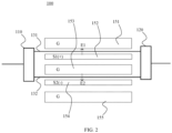
- an electro-optic modulator 100 includes a light splitting element 110; a light combining element 120; a first waveguide arm 131 and a second waveguide arm 132 that are arranged in parallel; and a first ground electrode 151, a first signal electrode 152, a second ground electrode 153, a second signal electrode 154, and a third ground electrode 155 that are arranged in sequence.
- the first signal electrode 152 and the second signal electrode 154 are configured to receive differential signals.
- the first waveguide arm 131 and the second waveguide arm 132 are connected between the light splitting element 110 and the light combining element 120.
- the first waveguide arm 131 is located between the first ground electrode 151 and the first signal electrode 152
- the second waveguide arm 132 is located between the second ground electrode 153 and the second signal electrode 154.
- the light splitting element 110 is not specifically limited in type, at least includes one input port and two output ports, and for example, may be a light splitting element with one input and two outputs.
- the light combining element 120 is not specifically limited in type, at least includes two input ports and one output port, and for example, may be a light combining element with two inputs and one output or a light combining element with two inputs and three outputs, etc..
- the first waveguide arm 131 is connected between one output port of the light splitting element 110 and one input port of the light combining element 120
- the second waveguide arm 132 is connected between the other output port of the light splitting element 110 and the other input port of the light combining element 120.
- the first ground electrode 151, the first signal electrode 152, the second ground electrode 153, the second signal electrode 154, and the third ground electrode 155 are arranged side by side, and for example, are arranged in parallel.
- the first signal electrode 152 and the second signal electrode 154 are configured to receive differential signals. That is, the first signal electrode 152 and the second signal electrode 154 respectively receive radio frequency voltage signals S1 and S2 that are of the same amplitude and opposite phases, and the radio frequency voltage signals S1 and S2 are differential signals.
- the materials of the first waveguide arm 131 and the second waveguide arm 132 include an electro-optic material, such as lithium niobate, lithium tantalate or potassium titanyl phosphate.
- an electro-optic material such as lithium niobate, lithium tantalate or potassium titanyl phosphate.
- the refractive index of the first waveguide arm 131 and the refractive index of the second waveguide arm 132 vary with the differential signals S1 and S2 received by the first signal electrode 152 and the second signal electrode 154, allowing the phases of the branch optical signals transmitted therein to be modulated, such that the two branch optical signals achieve a target phase difference when arriving at the light combining element 120.
- the target phase difference is, for example, an odd or even multiple of ⁇ .
- the second ground electrode 153 is arranged between the first signal electrode 152 and the second signal electrode 154, such that crosstalk that may be generated between the two signal electrodes can be shielded or reduced.
- the first signal electrode 152 and the second signal electrode 154 are independent of each other and are relatively far away from each other, which is also beneficial to reducing the crosstalk that may be generated between the two signal electrodes.
- the first signal electrode 152 is located between the first ground electrode 151 and the second ground electrode 153
- the second signal electrode 154 is located between the second ground electrode 153 and the third ground electrode 155, which can shield or reduce the crosstalk that may be caused to the signal electrodes by factors other than this group of electrodes.
- the electro-optic modulator 100 further includes a first independent waveguide section 133 and a second independent waveguide section 134 that are arranged in parallel with the first waveguide arm 131 and the second waveguide arm 132, where the first independent waveguide section 133 is located between the first signal electrode 152 and the second ground electrode 153, and the second independent waveguide section 134 is located between the second signal electrode 154 and the third ground electrode 155.
- the first independent waveguide section 133 and the second independent waveguide section 134 differ from the first waveguide arm 131 and the second waveguide arm 132 mainly in that the first independent waveguide section and the second independent waveguide section are not connected to other elements and are not configured to transmit optical signals.
- the first independent waveguide section 133 is positioned in an electric field E3 between the first signal electrode 152 and the second ground electrode 153
- the second independent waveguide section 134 is positioned in an electric field E4 between the second signal electrode 154 and the third ground electrode 155.
- the electric field E1 acts on the first waveguide arm 131
- the electric field E3 is opposite to the electric field E1 in direction and acts on the first independent waveguide section 133.
- the first independent waveguide section 133 is not configured to transmit optical signals
- the first independent waveguide section makes the effects of the electric fields E1 and E3 symmetrical, which can make the transmission of electrical signals of the two signal electrodes more stable, thus being beneficial to further reducing the transmission loss of the device.
- the electro-optic modulator 100 includes a substrate 210, an isolation layer 220, a waveguide layer 230, and an electrode layer 250 that are arranged in sequence, where the first waveguide arm 131 and the second waveguide arm 132 are located in the waveguide layer 230, and the first ground electrode 151, the first signal electrode 152, the second ground electrode 153, the second signal electrode 154, and the third ground electrode 155 are located in the electrode layer 250.
- the first independent waveguide section 133 and the second independent waveguide section 134 may alternatively be located in the waveguide layer 230 (not shown in the figure).
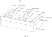
- the waveguide layer 230 may be a ridge waveguide layer as shown in FIG. 4 .
- the ridge waveguide layer includes a flat plate layer 2300 and a ridged layer 2310 located at a side of the flat plate layer 2300 away from the substrate 210.
- the flat plate layer 2300 and the ridged layer 2310 are of an integrated structure formed by etching, and the first waveguide arm 131 and the second waveguide arm 132 are located in the ridged layer 2310.
- the first independent waveguide section 133 and the second independent waveguide section 134 mentioned above may alternatively be located in the ridged layer 2310 (not shown in the figure).
- the first ground electrode 151, the first signal electrode 152, the second ground electrode 153, the second signal electrode 154, and the third ground electrode 155 are formed on a surface of a side of the flat plate layer 2300 away from the substrate 210, and are located in the same plane.
- the waveguide layer may alternatively be a ridged pattern layer, that is, the waveguide layer includes no flat plate layer, and the first waveguide arm, the second waveguide arm, the first independent waveguide section, and the second independent waveguide section mentioned above may be directly formed on a surface of the isolation layer away from the substrate.
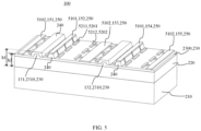
- the first signal electrode 152 and the second signal electrode 154 each include a first main electrode 5101 with a distance of h1 from the substrate 210, and the first ground electrode 151, the second ground electrode 153, and the third ground electrode 155 each include a second main electrode 5102 with a distance of h2 from the substrate 210, where h1 ⁇ h2, and h1 > h2, or h1 ⁇ h2.
- the electro-optic modulator 100 further includes a dielectric layer 240 located between the waveguide layer 230 and the electrode layer 250, and a dielectric constant of the dielectric layer 240 is less than that of the waveguide layer 230.
- the dielectric layer 240 may cover the first waveguide arm 131 and the second waveguide arm 132 as shown in the figure.
- a height difference between the first main electrode 5101 and the second main electrode 5102 may be formed by means of a pattern design of the dielectric layer 240.
- the waveguide layer 230 includes a flat plate layer 2300 and a ridged layer 2310 located at a side of the flat plate layer 2300 away from the substrate 210, the first main electrode 5101 is formed on a surface of a side of the dielectric layer 240 away from the substrate 210, and the second main electrode 5102 is formed on a surface of a side of the flat plate layer 2300 away from the substrate 210.
- the waveguide layer is a ridged pattern layer
- the first main electrode is formed on a surface of a side of the dielectric layer away from the substrate
- the second main electrode is formed on a surface of a side of the isolation layer away from the substrate.
- the height difference between the first main electrode and the second main electrode may alternatively be formed by means of a thickness difference of the flat plate layer of the waveguide layer in different regions.
- the electro-optic modulator may or may not include a dielectric layer.
- the waveguide layer includes a flat plate layer and a ridged layer located at a side of the flat plate layer away from the substrate, where the first waveguide arm and the second waveguide arm are located in the ridged layer, and the first main electrode or the second main electrode penetrates the flat plate layer and is in contact with the isolation layer.
- the height difference between the first main electrode and the second main electrode may also be implemented by means of this design.
- the main electrodes i.e., the first main electrodes 5101) of the first signal electrode 152 and the second signal electrode 154 are arranged at the same height, and the main electrodes (i.e., the second main electrodes 5102) of the first ground electrode 151, the second ground electrode 153, and the third ground electrode 155 are arranged at another height, which is beneficial to respective regulation of the signal electrodes and the ground electrodes, and makes regulation of electrical signal transmission more flexible and accurate, thereby reducing a difference in transmission speed between optical signals and electrical signals more easily and achieving good matching therebetween.
- each of the first signal electrode 152 and the second signal electrode 154 of the electro-optic modulator 100 further includes a first extension electrode 5201 correspondingly connected to the respective first main electrode 5101; and/or each of the first ground electrode 151, the second ground electrode 153, and the third ground electrode 155 further includes a second extension electrode 5202 correspondingly connected to the respective second main electrode 5102.
- each of the first signal electrode 152 and the second signal electrode 154 further includes a first extension electrode 5201 correspondingly connected to the respective first main electrode 5101, where the first extension electrode 5201 includes a plurality of first sub-electrodes 5211 (for example, T-shaped or L-shaped first sub-electrodes 5211) arranged at intervals in an extension direction of the first main electrode 5101.
- first sub-electrodes 5211 for example, T-shaped or L-shaped first sub-electrodes 5211
- Each of the first ground electrode 151, the second ground electrode 153, and the third ground electrode 155 further includes a second extension electrode 5202 correspondingly connected to the respective second main electrode 5102, where the second extension electrode 5202 includes a plurality of second sub-electrodes 5212 (for example, T-shaped or L-shaped second sub-electrodes 5212) arranged at intervals in the extension direction of the second main electrode 5102.
- the second extension electrode 5202 includes a plurality of second sub-electrodes 5212 (for example, T-shaped or L-shaped second sub-electrodes 5212) arranged at intervals in the extension direction of the second main electrode 5102.
- at least a part of the first extension electrode 5201 and at least a part of the second extension electrode 5202 are located in the same plane.
- first extension electrode 5201 and the second extension electrode 5202 are not limited to those shown in the figure.
- each of the first extension electrode 5201 and the second extension electrode 5202 may alternatively be a surface-shaped extension electrode in the same extension direction as the respective main electrode.
- the first waveguide arm 131 and the second waveguide arm 132 are located in the ridged layer 2310, and at least a part of the first extension electrode 5201 and at least a part of the second extension electrode 5202 are formed on a surface of a side of the flat plate layer 2300 away from the substrate 210. Since the first main electrode 5101 is separated from the flat plate layer 2300 by the dielectric layer 240, the first main electrode 5101 is raised, and thus the first extension electrode 5201 further includes a climbing portion along an etching cross-section of the dielectric layer 240.
- the waveguide layer is a ridged pattern layer
- at least a part of the first extension electrode and at least a part of the second extension electrode are formed on a surface of a side of the isolation layer away from the substrate. Since the first main electrode is separated from the isolation layer by the dielectric layer, the first main electrode is raised, and thus the first extension electrode further includes a climbing portion along an etching cross-section of the dielectric layer.
- the first ground electrode 151 includes one second extension electrode 5202 (including a plurality of second sub-electrodes 5212) arranged at a side of the first ground electrode 151 close to the first signal electrode 152, and the first signal electrode 152 includes two first extension electrodes 5201 (each including a plurality of first sub-electrodes 5211) distributed at two sides of the first signal electrode 152.
- the second ground electrode 153 includes two second extension electrodes 5202 (each including a plurality of second sub-electrodes 5212) distributed at two sides of the second ground electrode 153, and the second signal electrode 154 includes two first extension electrodes 5201 (each including a plurality of first sub-electrodes 5211) distributed at two sides of the second signal electrode 154.
- the third ground electrode 155 includes one second extension electrode 5202 (including a plurality of second sub-electrodes 5212) arranged at a side of the third ground electrode 155 close to the second signal electrode 154. Only some sub-electrodes are shown by reference signs.
- extension electrodes With the arrangement of the extension electrodes, intervals between the signal electrodes and the ground electrodes can be reduced, thus improving an electric field strength and reducing the transmission loss of electrical signals.
- some characteristics of the electrode structure (such as impedance and a transmission speed) are closely related to specific design parameters (such as a shape, a dimension, and the number) of the extension electrode.
- the design parameters of the extension electrode may be flexibly adjusted according to actual design requirements, so that the impedance of the electro-optic modulator 100 is as same as or close to that of the impedance at an input end thereof as possible, and the difference in transmission speeds of optical signals and electrical signals is compensated for to some extent, so that the transmission of the optical signals and the electrical signals can be matched as far as possible, thereby further improving performance of the electro-optic modulator 100.
- orientations or positional relationships or dimensions denoted by the terms such as “center”, “longitudinal”, “transverse”, “length”, “width”, “thickness”, “upper”, “lower”, “front”, “rear”, “left”, “right”, “vertical”, “horizontal”, “top”, “bottom”, “inner”, “outer”, “clockwise”, “counterclockwise”, “axial”, “radial” and “circumferential”, are the orientations or positional relationships or dimensions shown on the basis of the accompanying drawings, and these terms are used merely for ease of description, rather than indicating or implying that the device or element referred to must have particular orientations and be constructed and operated in the particular orientations, and therefore should not be construed as limiting the scope of protection of the present disclosure.
- first”, “second” and “third” are merely for descriptive purposes and should not be construed as indicating or implying relative importance or implicitly indicating the number of technical features indicated.
- the features defined with “first”, “second” and “third” may explicitly or implicitly include one or more features.
- the term “a plurality of” means two or more, unless otherwise explicitly and specifically defined.
- the terms such as “mounting”, “connection”, “connected” and “fixing” should be interpreted broadly, for example, they may be a fixed connection, a detachable connection, or an integrated connection; may be a mechanical connection, or an electrical connection, or communication; and may be a direct connection or an indirect connection by means of an intermediate medium, or may be internal communication between two elements or interaction between the two elements.
- the specific meanings of the above terms in the present disclosure can be understood according to specific circumstances.
- the expression of the first feature being “above” or “below” the second feature may include the case that the first feature is in direct contact with the second feature, or the case that the first feature and the second feature are not in direct contact but are contacted via another feature therebetween.
- the first feature being “over”, “above” or “on” the second feature includes the case that the first feature is directly or obliquely above the second feature, or merely indicates that the first feature is at a higher level than the second feature.
- the first feature being “below”, “under” or “beneath” the second feature includes the case that the first feature is directly or obliquely below the second feature, or merely indicates that the first feature is at a lower level than the second feature.
Landscapes
- Physics & Mathematics (AREA)
- Nonlinear Science (AREA)
- General Physics & Mathematics (AREA)
- Optics & Photonics (AREA)
- Chemical & Material Sciences (AREA)
- Engineering & Computer Science (AREA)
- Ceramic Engineering (AREA)
- Crystallography & Structural Chemistry (AREA)
- Electromagnetism (AREA)
- Optical Modulation, Optical Deflection, Nonlinear Optics, Optical Demodulation, Optical Logic Elements (AREA)
Applications Claiming Priority (2)
| Application Number | Priority Date | Filing Date | Title |
|---|---|---|---|
| CN202210179793.2A CN116699881A (zh) | 2022-02-25 | 2022-02-25 | 电光调制器 |
| PCT/CN2023/074961 WO2023160392A1 (zh) | 2022-02-25 | 2023-02-08 | 电光调制器 |
Publications (2)
| Publication Number | Publication Date |
|---|---|
| EP4435502A1 true EP4435502A1 (de) | 2024-09-25 |
| EP4435502A4 EP4435502A4 (de) | 2025-03-19 |
Family
ID=87764802
Family Applications (1)
| Application Number | Title | Priority Date | Filing Date |
|---|---|---|---|
| EP23759017.9A Pending EP4435502A4 (de) | 2022-02-25 | 2023-02-08 | Elektrooptischer modulator |
Country Status (5)
| Country | Link |
|---|---|
| US (1) | US20250147379A1 (de) |
| EP (1) | EP4435502A4 (de) |
| JP (1) | JP7739627B2 (de) |
| CN (1) | CN116699881A (de) |
| WO (1) | WO2023160392A1 (de) |
Families Citing this family (4)
| Publication number | Priority date | Publication date | Assignee | Title |
|---|---|---|---|---|
| CN119667979A (zh) * | 2023-09-12 | 2025-03-21 | 南京刻得不错光电科技有限公司 | 电光调制器及光发射器 |
| CN220829639U (zh) * | 2023-09-18 | 2024-04-23 | 苏州旭创科技有限公司 | 光调制器 |
| JP2025152561A (ja) * | 2024-03-28 | 2025-10-10 | 住友大阪セメント株式会社 | 光変調器 |
| CN117991524B (zh) * | 2024-04-07 | 2024-07-30 | 鹏城实验室 | 一种差分驱动薄膜铌酸锂电光调制器芯片 |
Family Cites Families (11)
| Publication number | Priority date | Publication date | Assignee | Title |
|---|---|---|---|---|
| US6192167B1 (en) * | 1998-07-24 | 2001-02-20 | Uniphase Telecommunications Products | Differential drive optical modulator |
| EP2116889B1 (de) * | 2007-03-06 | 2014-08-06 | NGK Insulators, Ltd. | Optischer phasenmodulator |
| JP2009086336A (ja) * | 2007-09-28 | 2009-04-23 | Sumitomo Osaka Cement Co Ltd | 光導波路型デバイス |
| US8849071B2 (en) * | 2009-12-30 | 2014-09-30 | Jds Uniphase Corporation | Optical waveguide modulator |
| US8224143B2 (en) * | 2010-02-05 | 2012-07-17 | Advantest Corporation | Substrate structure and manufacturing method |
| EP3432058B1 (de) * | 2016-03-18 | 2020-08-05 | Nippon Telegraph And Telephone Corporation | Optischer modulator |
| CN111665646B (zh) * | 2019-03-08 | 2021-08-31 | 中兴光电子技术有限公司 | 电极慢波结构、具有慢波结构的电极组件及电光调制器 |
| JP7283180B2 (ja) * | 2019-03-29 | 2023-05-30 | 住友大阪セメント株式会社 | 光変調器 |
| CN114981694B (zh) * | 2019-11-27 | 2025-09-16 | 超光公司 | 具有工程化电极的电光器件 |
| CN111505845A (zh) * | 2020-05-14 | 2020-08-07 | 苏州极刻光核科技有限公司 | 一种共面波导线电极结构及调制器 |
| CN114019703A (zh) * | 2021-11-22 | 2022-02-08 | 东南大学 | 一种薄膜铌酸锂双平行电光调制器集成芯片 |
-
2022
- 2022-02-25 CN CN202210179793.2A patent/CN116699881A/zh active Pending
-
2023
- 2023-02-08 WO PCT/CN2023/074961 patent/WO2023160392A1/zh not_active Ceased
- 2023-02-08 JP JP2024540654A patent/JP7739627B2/ja active Active
- 2023-02-08 US US18/720,308 patent/US20250147379A1/en active Pending
- 2023-02-08 EP EP23759017.9A patent/EP4435502A4/de active Pending
Also Published As
| Publication number | Publication date |
|---|---|
| JP2025501344A (ja) | 2025-01-17 |
| CN116699881A (zh) | 2023-09-05 |
| JP7739627B2 (ja) | 2025-09-16 |
| WO2023160392A1 (zh) | 2023-08-31 |
| EP4435502A4 (de) | 2025-03-19 |
| US20250147379A1 (en) | 2025-05-08 |
Similar Documents
| Publication | Publication Date | Title |
|---|---|---|
| EP4435502A1 (de) | Elektrooptischer modulator | |
| US6483953B1 (en) | External optical modulation using non-co-linear compensation networks | |
| US20240377664A1 (en) | Electro-optic modulator and electro-optic device | |
| US12591163B2 (en) | Electro-optic modulator | |
| EP4350426A1 (de) | Wellenleiterleitungselektrodenstruktur und elektrooptischer modulator | |
| CN206178309U (zh) | 光调制器及光调制系统 | |
| CN113467106A (zh) | 折叠型马赫曾德尔调制器 | |
| US6646776B1 (en) | Suppression of high frequency resonance in an electro-optical modulator | |
| CN117991526B (zh) | 一种双驱动差分薄膜铌酸锂电光调制器芯片 | |
| EP4379457A1 (de) | Gefalteter elektrooptischer modulator | |
| CN111610596B (zh) | 高边带抑制比的双驱m-z光学单边带调制器 | |
| US20240345423A1 (en) | Phase modulation module and electro-optic modulator | |
| US6885780B2 (en) | Suppression of high frequency resonance in an electro-optical modulator | |
| CN219676399U (zh) | 电光调制器 | |
| JP7796863B2 (ja) | 電気光学変調器および電気光学デバイス | |
| US20250298284A1 (en) | Electro-optic modulator | |
| JP2015212769A (ja) | 半導体マッハツェンダ光変調器 | |
| US20240393626A1 (en) | Electro-optic modulator and electro-optic device | |
| US20250323731A1 (en) | Optical-mode modulation device and photonic chip | |
| JP2012128007A (ja) | 光変調器 | |
| CN117471718A (zh) | 电光调制器 | |
| CN115903284A (zh) | 电光调制器 | |
| Yamamoto et al. | LiNbO 3 optical SSB modulator using microwave branchline coupler miniaturized by inter-digital capacitors |
Legal Events
| Date | Code | Title | Description |
|---|---|---|---|
| STAA | Information on the status of an ep patent application or granted ep patent |
Free format text: STATUS: THE INTERNATIONAL PUBLICATION HAS BEEN MADE |
|
| PUAI | Public reference made under article 153(3) epc to a published international application that has entered the european phase |
Free format text: ORIGINAL CODE: 0009012 |
|
| STAA | Information on the status of an ep patent application or granted ep patent |
Free format text: STATUS: REQUEST FOR EXAMINATION WAS MADE |
|
| 17P | Request for examination filed |
Effective date: 20240617 |
|
| AK | Designated contracting states |
Kind code of ref document: A1 Designated state(s): AL AT BE BG CH CY CZ DE DK EE ES FI FR GB GR HR HU IE IS IT LI LT LU LV MC ME MK MT NL NO PL PT RO RS SE SI SK SM TR |
|
| A4 | Supplementary search report drawn up and despatched |
Effective date: 20250218 |
|
| RIC1 | Information provided on ipc code assigned before grant |
Ipc: G02F 1/03 20060101AFI20250212BHEP |
|
| RAP1 | Party data changed (applicant data changed or rights of an application transferred) |
Owner name: NANJING LYCORE TECHNOLOGIES CO., LTD. |
|
| DAV | Request for validation of the european patent (deleted) | ||
| DAX | Request for extension of the european patent (deleted) |