EP4435810A2 - Composant électronique multicouche - Google Patents
Composant électronique multicouche Download PDFInfo
- Publication number
- EP4435810A2 EP4435810A2 EP24158361.6A EP24158361A EP4435810A2 EP 4435810 A2 EP4435810 A2 EP 4435810A2 EP 24158361 A EP24158361 A EP 24158361A EP 4435810 A2 EP4435810 A2 EP 4435810A2
- Authority
- EP
- European Patent Office
- Prior art keywords
- layer
- electrode
- electronic component
- plating portion
- disposed
- Prior art date
- Legal status (The legal status is an assumption and is not a legal conclusion. Google has not performed a legal analysis and makes no representation as to the accuracy of the status listed.)
- Pending
Links
Images


Classifications
-
- H—ELECTRICITY
- H01—ELECTRIC ELEMENTS
- H01G—CAPACITORS; CAPACITORS, RECTIFIERS, DETECTORS, SWITCHING DEVICES, LIGHT-SENSITIVE OR TEMPERATURE-SENSITIVE DEVICES OF THE ELECTROLYTIC TYPE
- H01G4/00—Fixed capacitors; Processes of their manufacture
- H01G4/002—Details
- H01G4/228—Terminals
- H01G4/232—Terminals electrically connecting two or more layers of a stacked or rolled capacitor
-
- H—ELECTRICITY
- H01—ELECTRIC ELEMENTS
- H01G—CAPACITORS; CAPACITORS, RECTIFIERS, DETECTORS, SWITCHING DEVICES, LIGHT-SENSITIVE OR TEMPERATURE-SENSITIVE DEVICES OF THE ELECTROLYTIC TYPE
- H01G4/00—Fixed capacitors; Processes of their manufacture
- H01G4/002—Details
- H01G4/018—Dielectrics
- H01G4/06—Solid dielectrics
- H01G4/08—Inorganic dielectrics
- H01G4/12—Ceramic dielectrics
- H01G4/1209—Ceramic dielectrics characterised by the ceramic dielectric material
- H01G4/1218—Ceramic dielectrics characterised by the ceramic dielectric material based on titanium oxides or titanates
- H01G4/1227—Ceramic dielectrics characterised by the ceramic dielectric material based on titanium oxides or titanates based on alkaline earth titanates
-
- H—ELECTRICITY
- H01—ELECTRIC ELEMENTS
- H01G—CAPACITORS; CAPACITORS, RECTIFIERS, DETECTORS, SWITCHING DEVICES, LIGHT-SENSITIVE OR TEMPERATURE-SENSITIVE DEVICES OF THE ELECTROLYTIC TYPE
- H01G4/00—Fixed capacitors; Processes of their manufacture
- H01G4/30—Stacked capacitors
-
- H—ELECTRICITY
- H01—ELECTRIC ELEMENTS
- H01G—CAPACITORS; CAPACITORS, RECTIFIERS, DETECTORS, SWITCHING DEVICES, LIGHT-SENSITIVE OR TEMPERATURE-SENSITIVE DEVICES OF THE ELECTROLYTIC TYPE
- H01G2/00—Details of capacitors not covered by a single one of groups H01G4/00-H01G11/00
- H01G2/02—Mountings
- H01G2/06—Mountings specially adapted for mounting on a printed-circuit support
- H01G2/065—Mountings specially adapted for mounting on a printed-circuit support for surface mounting, e.g. chip capacitors
-
- H—ELECTRICITY
- H01—ELECTRIC ELEMENTS
- H01G—CAPACITORS; CAPACITORS, RECTIFIERS, DETECTORS, SWITCHING DEVICES, LIGHT-SENSITIVE OR TEMPERATURE-SENSITIVE DEVICES OF THE ELECTROLYTIC TYPE
- H01G4/00—Fixed capacitors; Processes of their manufacture
- H01G4/002—Details
- H01G4/005—Electrodes
- H01G4/008—Selection of materials
-
- H—ELECTRICITY
- H01—ELECTRIC ELEMENTS
- H01G—CAPACITORS; CAPACITORS, RECTIFIERS, DETECTORS, SWITCHING DEVICES, LIGHT-SENSITIVE OR TEMPERATURE-SENSITIVE DEVICES OF THE ELECTROLYTIC TYPE
- H01G4/00—Fixed capacitors; Processes of their manufacture
- H01G4/002—Details
- H01G4/005—Electrodes
- H01G4/012—Form of non-self-supporting electrodes
-
- H—ELECTRICITY
- H01—ELECTRIC ELEMENTS
- H01G—CAPACITORS; CAPACITORS, RECTIFIERS, DETECTORS, SWITCHING DEVICES, LIGHT-SENSITIVE OR TEMPERATURE-SENSITIVE DEVICES OF THE ELECTROLYTIC TYPE
- H01G4/00—Fixed capacitors; Processes of their manufacture
- H01G4/002—Details
- H01G4/228—Terminals
- H01G4/232—Terminals electrically connecting two or more layers of a stacked or rolled capacitor
- H01G4/2325—Terminals electrically connecting two or more layers of a stacked or rolled capacitor characterised by the material of the terminals
-
- H—ELECTRICITY
- H01—ELECTRIC ELEMENTS
- H01G—CAPACITORS; CAPACITORS, RECTIFIERS, DETECTORS, SWITCHING DEVICES, LIGHT-SENSITIVE OR TEMPERATURE-SENSITIVE DEVICES OF THE ELECTROLYTIC TYPE
- H01G4/00—Fixed capacitors; Processes of their manufacture
- H01G4/002—Details
- H01G4/018—Dielectrics
- H01G4/06—Solid dielectrics
- H01G4/08—Inorganic dielectrics
- H01G4/12—Ceramic dielectrics
Definitions
- the present disclosure relates to a multilayer electronic component.
- a multilayer ceramic capacitor (MLCC), a multilayer electronic component may be a chip-type condenser mounted on the printed circuit boards of various electronic products such as a liquid crystal display (LCD) and a plasma display panel (PDP), a computer, a smartphone, and charging or discharging electricity.
- LCD liquid crystal display
- PDP plasma display panel
- a Ni plating layer and a Sn plating layer may be formed in order on a Cu electrode layer.
- forming a plating layer without defects such as plating layer breakage or void formation in the plating layer may have a significant impact on improving moisture resistance reliability of the multilayer electronic component.
- An example embodiment of the present disclosure is to address deterioration of moisture resistance reliability of a multilayer electronic component due to hydrogen formed when a plating layer is formed on an external electrode.
- a multilayer electronic component includes a body including a dielectric layer and an internal electrode alternately disposed with the dielectric layer; and an external electrode disposed on the body, wherein the external electrode includes an electrode layer connected to the internal electrode and including Cu, a first plating portion disposed on the electrode layer, and a second plating portion disposed on the first plating portion, and wherein the first plating portion includes a Ni layer in contact with the electrode layer and including Ni, and an intermetallic compound layer disposed on the Ni layer and including an intermetallic compound including at least one of Ni and Sn
- a first direction may be defined as a direction in which first and second internal electrodes are alternately disposed with a dielectric layer interposed therebetween or a thickness T direction, among second and third directions perpendicular to the first direction, a second direction may be defined as a length L direction, and a third direction may be defined as a width W direction.
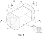
- FIG. 1 is a perspective diagram illustrating a multilayer electronic component according to an example embodiment.
- FIG. 2 is a cross-sectional diagram taken along line I-I' in FIG. 1 .
- FIG. 3 is a cross-sectional diagram taken along line II-II' in FIG. 1 .
- FIG. 4 is an exploded perspective diagram illustrating a body according to an example embodiment of the present disclosure.
- FIG. 5 is an enlarged diagram illustrating region P in FIG. 2 .
- the multilayer electronic component 100 according to an example embodiment will be described in greater detail with reference to FIGS. 1 to 5 .
- a multilayer electronic component 100 may include a body 110 including a dielectric layer 111 and internal electrodes 121, 122 alternately disposed with the dielectric layer; and external electrodes 130, 140 disposed on the body.
- the external electrode includes an electrode layer 131 connected to the internal electrode and including Cu, a first plating portion 132 disposed on the electrode layer, and a second plating portion 133 disposed on the first plating portion, and the first plating portion includes a Ni layer 132a in contact with the electrode layer and including Ni, and an intermetallic compound layer 132b disposed on the Ni layer and including an intermetallic compound including at least one of Ni and Sn.
- the body 110 may include a dielectric layer 111 and internal electrodes 121 and 122 alternately disposed with the dielectric layer 111.
- the body 110 may have dielectric layers 111 and internal electrodes 121 and 122 laminated alternately, and the direction in which the dielectric layers 111 and the internal electrodes 121 and 122 are laminated may be defined as the first direction.
- the shape of the body 110 may not be limited to any particular shape, but as illustrated, the body 110 may have a hexahedral shape or a shape similar to a hexahedral shape. Due to reduction of ceramic powder included in the body 110 during a firing process, the body 110 may not have an exact hexahedral shape formed by linear lines but may have a substantially hexahedral shape.
- the body 110 may have first and second surfaces 1 and 2 opposing each other in the first direction, third and fourth surfaces 3 and 4 connected to the first and second surfaces 1 and 2 and opposing in the second direction, and fifth and sixth surfaces 5 and 6 connected to the first and second surfaces 1 and 2 and the third and fourth surfaces 3 and 4 and opposing each other in the third direction.
- the plurality of dielectric layers 111 forming the body 110 may be in a fired state, and a boundary between the adjacent dielectric layers 111 may be integrated with each other such that the boundary may not be distinct without using a scanning electron microscope (SEM).
- SEM scanning electron microscope
- a raw material for forming the dielectric layer 111 is not limited to any particular example as long as sufficient capacitance may be obtained.
- a barium titanate-based material, a lead composite perovskite-based material, or a strontium titanate-based material may be used.
- the barium titanate material may include BaTiO 3 ceramic powder, and an example of the ceramic powder may include (Ba 1-x Ca x )TiO 3 (0 ⁇ x ⁇ 1), Ba(Ti 1-y Ca y )O 3 (0 ⁇ y ⁇ 1), (Ba 1-x Ca x )(Ti 1-y Zr y )O 3 (0 ⁇ x ⁇ 1, 0 ⁇ y ⁇ 1) or Ba(Ti 1-y Zr y )O 3 (0 ⁇ y ⁇ 1) in which Ca (calcium), Zr (zirconium) is partially solid-solute.
- various ceramic additives, organic solvents, binders, dispersants, or the like may be added to a raw material for forming the dielectric layer 111 in the embodiment to powder such as barium titanate (BaTiO 3 ).
- the average thickness td of the dielectric layer 111 may not be limited to any particular example.
- the average thickness td of the dielectric layer 111 may be 0.2 um or more and 2 um or less (i.e., in a range from 0.2 ⁇ m to 2 ⁇ m).
- the average thickness td of the dielectric layer 111 may be 0.35 um or less.
- the average thickness td of the dielectric layer 111 may refer to the average size of the dielectric layer 111 disposed between the first and second internal electrodes 121 and 122 in the first direction.
- the average thickness td of the dielectric layer 111 may refer to the average thickness of at least one of the plurality of dielectric layers 111.
- the average thickness td of the dielectric layer 111 may be measured by scanning a cross-section of the body 110 in the length and thickness directions (L-T) using a scanning electron microscope (SEM) with a magnification of 10,000. More specifically, an average value may be measured from the thicknesses of the dielectric layer 111 at 30 points spaced apart by an equal distance in the length direction in the scanned image. The 30 points at equal distances may be designated in the active portion Ac. Also, when the average value is measured by extending the measurement of the average value to ten dielectric layers 111, the average thickness of the dielectric layer 111 may be further generalized.
- the body 110 may include a capacitance forming portion Ac disposed in the body 110, which may be a region in which the first and second internal electrodes 121 and 122 overlap in the first direction.
- the capacitance forming portion Ac may contribute to capacitance formation of a capacitor, and may be formed by repeatedly laminating a plurality of first and second internal electrodes 121 and 122 with a dielectric layer 111 interposed therebetween.
- An upper cover portion 112 may be disposed on one surface of the capacitance forming portion Ac in the first direction, and a lower cover portion 113 may be included on another surface opposing the one surface of the capacitance forming portion Ac in the first direction.
- the upper cover portion 112 and the lower cover portion 113 may be formed by laminating a single dielectric layer or two or more dielectric layers on the upper and lower surfaces of the capacitance forming portion Ac in the thickness direction, respectively, and may prevent damages to the internal electrode due to physical or chemical stress.
- the upper cover portion 112 and the lower cover portion 113 may not include internal electrodes and may include the same material as that of the dielectric layer 111.
- the upper cover portion 112 and the lower cover portion 113 may include a ceramic material, for example, a barium titanate (BaTiO 3 ) ceramic material.
- the average thickness of the cover portion 112 and 113 may not be limited to any particular example. However, to easily obtain miniaturization and high capacitance of the multilayer electronic component, the average thickness tc of the cover portions 112 and 113 may be 15 um or less. Here, the average thickness of the cover portions 112 and 113 may refer to the average thickness of each of the first cover portion 112 and the second cover portion 113.
- the average thickness Tc of the cover portion 112 and 113 may refer to the size in the first direction, and may be a value obtained by averaging the size of the cover portion 112 and 113 in the first direction measured at 5 points spaced apart by an equal distance in the upper or lower portions of the capacitance forming portion Ac.
- margin portions 114 and 115 may be disposed on one surface and another surface opposing the one surface of the capacitance forming portion Ac in the third direction.
- the margin portions 114 and 115 may include a margin portion 114 disposed on the fifth surface 5 and a margin portion 115 disposed on the sixth surface 6 of the body 110. That is, the margin portions 114 and 115 may be disposed on both side surfaces of the body 110 in the width direction.
- the margin portions 114 and 115 may refer to a region between both ends of the first and second internal electrodes 121 and 122 and the boundary surface of the body 110 in a cross-section of the body 110 taken in the width-thickness (W-T) direction.
- the margin portions 114 and 115 may prevent damages to the internal electrode due to physical or chemical stress.
- the margin portions 114 and 115 may be formed by forming internal electrodes by applying a conductive paste on the ceramic green sheet other than the region in which the margin portions are formed.
- the internal electrodes may be cut out to be exposed to the fifth and sixth surfaces 5 and 6 of the body, a single dielectric layer or two or more dielectric layers may be laminated on both side surfaces of the capacitance forming portion Ac in the third direction (width direction), thereby forming the margin portions 114 and 115.
- the width of the margin portion 114 and 115 may not be limited to any particular example. However, the average width of the margin portions 114 and 115 may be 15 um or less to easily obtain miniaturization and high capacitance of the multilayer electronic component.
- the average width of the margin portion 114 and 115 may refer to the average size of the margin portion 114 and 115 in the third direction, and may be a value obtained by averaging the size of the margin portion 114 and 115 in the third direction measured at 5 points spaced apart by an equal distance on the side of the capacitance forming portion Ac.
- the internal electrodes 121 and 122 may be alternately laminated with the dielectric layer 111. In this case, the internal electrode and the dielectric layers may be alternately disposed in the first direction.
- the internal electrodes 121 and 122 may include a first internal electrode 121 and a second internal electrode 122.
- the first and second internal electrodes 121 and 122 may be alternately disposed to oppose each other with the dielectric layer 111 included in the body 110 interposed therebetween, and may be connected to the third and fourth surfaces 3 and 4 of the body 110, respectively.
- one end of the first internal electrode 121 may be connected to the third surface
- one end of the second internal electrode 122 may be connected to the fourth surface. That is, in an example embodiment, the internal electrodes 121 and 122 may be in contact with the third surface 3 or the fourth surface 4.
- the first internal electrode 121 may be spaced apart from the fourth surface 4 and may be exposed through the third surface 3, and the second internal electrode 122 may be spaced apart from the third surface 3 and may be exposed through the fourth surface 4.
- the first external electrode 131 may be disposed on the third surface 3 of the body 110 and may be connected to the first internal electrode 121, and the second external electrode 132 may be disposed on the fourth surface 4 of the body 110 and may be connected to the second internal electrode 122.
- the first internal electrode 121 may not be connected to the second external electrode 140 and may be connected to the first external electrode 130, and the second internal electrode 122 may not be connected to the first external electrode 130 and may be connected to the second external electrode 140. Accordingly, the first internal electrode 121 may be spaced apart from the fourth surface 4 by a predetermined distance, and the second internal electrode 122 may be spaced apart from the third surface 3 by a predetermined distance. In this case, the first and second internal electrodes 121 and 122 may be electrically separated from each other by the dielectric layer 111 disposed therebetween.
- the material for forming the internal electrodes 121 and 122 is not limited to any particular example, and a material having excellent electrical conductivity may be used.
- the internal electrodes 121 and 122 may include one or more of nickel (Ni), copper (Cu), palladium (Pd), silver (Ag), gold (Au), platinum (Pt), tin (Sn), tungsten (W), titanium (Ti), and alloys thereof.
- the internal electrodes 121 and 122 may be formed by printing conductive paste for internal electrodes including one or more of nickel (Ni), copper (Cu), palladium (Pd), silver (Ag), gold (Au), platinum (Pt), tin (Sn), tungsten (W), titanium (Ti), and alloys thereof on a ceramic green sheet.
- a screen-printing method or a gravure printing method may be used as a method of printing the conductive paste for internal electrodes, but an example embodiment thereof is not limited thereto.
- the average thickness te of the internal electrodes 121 and 122 may not need to be limited to any particular example.
- the average thickness te of the internal electrodes 121 and 122 may be 0.2 um or more and 2 um or less (i.e., in a range from 0.2 ⁇ m to 2 ⁇ m).
- the average thickness te of the internal electrodes 121 and 122 may be 0.35 ⁇ m.
- the average thickness te of the internal electrodes 121 and 122 may refer to the average thickness te of the internal electrodes 121 and 122.
- the average thickness td of the internal electrodes 121 and 122 may refer to the average thickness of at least one of the plurality of internal electrodes 121 and 122.
- the average thickness te of the internal electrodes 121 and 122 may be measured by scanning a cross-section of the body 110 in the length and thickness direction (L-T) using a scanning electron microscope (SEM) with a magnification of 10,000. More specifically, an average value may be measured from the thicknesses of the internal electrodes 121 and 122 at 30 points spaced apart by an equal distance in the second direction in the scanned image. The 30 points at equal distances may be designated in the active portion Ac. Also, when the average value is measured by extending the measurement of the average value to ten internal electrodes 121 and 122, the average thickness of the internal electrodes 121 and 122 may be further generalized.
- the external electrodes 131 and 132 may be disposed on the body 110.
- the external electrodes 130 and 140 may include a first external electrode 130 disposed on the third surface 3 of the body 110 and a second external electrode 140 disposed on the fourth surface 4 of the body 110.
- the structures of the external electrodes 130 and 140 in the example embodiment will be described in greater detail with respect to the first external electrode 130.
- the description of the first external electrode 130 may also be applied to the second external electrode 140.
- a structure in which the multilayer electronic component 100 has two external electrodes 131 and 132 is described, but the number or the shape of the external electrodes 131 and 132 may change depending on the shape of the internal electrodes 121 and 122 or other purposes.
- the external electrode 130 may include an electrode layer 131 connected to the internal electrode 121 and including Cu, a first plating portion 132 disposed on the electrode layer, and a second plating portion 133 disposed on the first plating portion 132.
- the first plating portion may include a Ni layer 132a in contact with the electrode layer and including Ni, and an intermetallic compound layer 132b disposed on the Ni layer and including an intermetallic compound including at least one of Ni and Sn.
- the electrode layer 131 may be connected to the internal electrode 121 and may include Cu.
- the electrode layer 131 may secure electrical connectivity from the external electrode 130 to the internal electrode 121.
- the electrode layer 131 may further include at least one of a conductive metal element and an alloy other than Cu in example embodiments.
- the electrode layer 131 may include at least one of Ni, Pd, Cr, and alloys thereof in addition to Cu.
- the method of forming the electrode layer 131 is not limited to any particular example.
- the electrode layer 131 may be formed by applying a conductive paste including Cu particles and glass to the third surface 3 and fourth surface 4 of the body 110 and performing a drying and firing process, but an example embodiment thereof is not limited thereto.
- the electrode layer 131 may be formed by applying Cu to the third surface 3 and the fourth surface 4 of the body 110 through electrolytic plating or electroless plating. That is, the electrode layer 131 may be a fired electrode further including glass or a plating electrode not including glass, but an example embodiment thereof is not limited thereto.
- the plating layer of the external electrode included in the multilayer electronic component may be formed by electroplating.
- hydrogen may be likely to be formed, and hydrogen formed as above may penetrate into the body 110, such that electrical properties of the entire multilayer electronic component 100 may be deteriorated.
- a Ni-Sn alloy layer may be formed on an electrode layer including Cu.
- an interfacial void defect may occur due to a difference in diffusion rates between Cu and Sn.
- the defects may become a main penetration path of moisture and hydrogen, and may cause a decrease in moisture resistance reliability of a multilayer electronic component.
- the Ni-Sn alloy layer rather than directly forming the Ni-Sn alloy layer on the electrode layer 131 including Cu, by disposing a layer between the electrode layer 131 and the Ni-Sn alloy layer, interfacial void defects due to the difference in diffusion rates between Cu and Sn may be suppressed, and moisture and hydrogen may be prevented from diffusing into the body 110, such that moisture resistance reliability of the multilayer electronic component 100 may improve.
- the electrode layer 131 connected to the internal electrode 121 and including Cu and the Ni layer 132a including Ni may be disposed to be in contact with each other, and an intermetallic compound layer 132b including an intermetallic compound including at least one of Ni and Sn on the Ni layer 132a may be disposed, such that direct contact between the electrode layer 131 and the intermetallic compound layer 132b may be prevented, and void defects due to a difference in diffusion rates between Cu and Sn may be prevented. Accordingly, penetration of hydrogen and moisture into the body 110 may be effectively suppressed, and void defects between the electrode layer 131 and the first plating portion 132 may be prevented. Accordingly, moisture resistance reliability of the multilayer electronic component 100 may be significantly improved.
- the method of forming the first plating portion 132 is not limited to any particular example.
- the first plating portion 132 may be formed by plating the Ni layer 132a on the electrode layer 131 using electroplating or electroless plating, and plating intermetallic compound layer 132b using alloy plating.
- hydrogen which may be generated when the Ni layer 132a is formed by electroplating may be removed by performing a heat treatment after forming the intermetallic compound layer 132b.
- intermetallic compound layer 132b The type of intermetallic compound including at least one of Ni and Sn included in intermetallic compound layer 132b is not limited to any particular example.
- the intermetallic compound may include at least one of Ni 3 Sn, Ni 3 Sn 2 and Ni 3 Sn 4 .
- the average thickness T1 of the first plating portion 132 is not limited to any particular example. However, the average thickness T1 of the first plating portion 132 may be preferably 0.3 um or more to sufficiently cover the surface of the electrode layer 131. An upper limit of the average thickness T1 of the first plating portion 132 is not limited to any particular example, and may be preferably 5 um or less for miniaturization of the multilayer electronic component 100. In other words, the average thickness T1 of the first plating portion 132 may be in a range from 0.3 ⁇ m to 5 ⁇ m.
- the second plating portion 133 may be disposed on the first plating portion 132.
- the second plating portion 133 may further improve sealing properties or mounting properties of the external electrode 130.
- the second plating portion 133 may include an Ni layer 133a in contact with the first plating portion 132 and including Ni, and an Sn layer 133b disposed on the Ni layer 133a of the second plating portion 133 and including Sn. Accordingly, sealing properties of the multilayer electronic component 100 may be further improved, and mounting properties may also be improved.
- a method of forming the second plating portion 133 is not limited to any particular example, and may be formed using various plating methods such as electroless plating and electroplating.
- An average thickness T1a of the Ni layer 132a of the first plating portion 132 may be greater than an average thickness T2a of the Ni layer 133a of the second plating portion 133. Accordingly, the electrostatic capacity per unit volume of the multilayer electronic component 100 may be improved by reducing the proportion of the first plating portion 132 in the external electrode 130.
- a method of measuring the average thickness T1 of the first plating portion 132, the average thickness T1a of the Ni layer 132a of the first plating portion 132, and the average thickness T2a of the Ni layer 133a of the second plating portion 133 are not limited to any particular example.
- the value may be obtained by exposing cross-sections in the first and second directions by FIB milling up to the central portion of the multilayer electronic component 100 in third direction, dividing the region into 5 portions in the first direction from an uppermost end to a lowermost end of the internal electrodes 121 and 122, and averaging the size in the second direction measured using energy dispersive X-ray spectrometry (SEM-EDX) Ion mode at random points in each region.
- SEM-EDX energy dispersive X-ray spectrometry
- recognition of the layers may be carried out by identifying the composition through SEM-EDX analysis.
- the presence or absence of an intermetallic compound including at least one of Ni and Sn may be determined through SEM-EDX analysis and X-Ray diffraction (XRD) analysis.
- FIG. 6 is a cross-sectional diagram illustrating a multilayer electronic component according to an example embodiment of the present disclosure, corresponding to the cross-sectional diagram taken along line I-I' in FIG. 1 .
- FIG. 7 is an enlarged diagram illustrating region Q in FIG. 6 .
- the multilayer electronic component 100' according to another example embodiment and various example embodiments will be described in detail with reference to FIGS. 6 and 7 .
- the descriptions overlapping the multilayer electronic component 100 according to an example embodiment will not be provided.
- the multilayer electronic component 100' may have substantially the same configuration as that of the multilayer electronic component 100 according to an example embodiment, other than the structure of the first plating portion 132.
- the multilayer electronic component 100' may include a body 110 including a dielectric layer 111 and internal electrodes 121 and 122 alternately disposed with the dielectric layer; and external electrodes 130 and 140 disposed on the body, wherein the external electrode includes an electrode layer 131 connected to the internal electrode and including Cu, a first plating portion disposed on the electrode layer, and a second plating portion 132 disposed on the first plating portion, and the first plating portion includes an Ni layer 132a in contact with the electrode layer and including Ni, an intermetallic compound layer 132b disposed on the Ni layer and including an intermetallic compound including at least one of Ni and Sn, and an Sn layer 132c disposed on the intermetallic compound layer and including Sn.
- the Ni layer 132a including Ni and the Sn layer 132c including Sn may be formed in order on the electrode layer 131, and the intermetallic compound layer 132b including an intermetallic compound including Ni and Sn may be formed on the interfacial surface of Ni layer 132a and Sn layer 132c through a heat treatment. Accordingly, hydrogen generated when the Ni layer 132a and Sn layer 132c are formed by electroplating in the process of forming the intermetallic compound layer 132b may be removed, thereby improving moisture resistance reliability of the multilayer electronic component 100'.
- the average thickness T1' of the first plating portion 132 is not limited to any particular example. However, the average thickness T1' of the first plating portion 132 may be preferably 0.5 um or more to sufficiently cover the surface of the electrode layer 131. An upper limit of the average thickness T1' of the first plating portion 132 is not limited to any particular example, and may be preferably 5 ⁇ m or less for miniaturization of the multilayer electronic component 100. In other words, the average thickness T1' of the first plating portion 132 may be in a range from 0.5 ⁇ m to 5 ⁇ m.
- the average thickness T1a' of the Ni layer 132a of the first plating portion 132 may be smaller than the average thickness T2a' of the Ni layer 133a of the second plating portion 133. Accordingly, capacitance per unit volume of the multilayer electronic component 100 may be improved by reducing the proportion of the first plating portion 132 in the external electrode 130.
- the average thickness T1b' of the Sn layer 132c of the first plating portion 132 may be smaller than the average thickness T2b' of the Sn layer 133b of the second plating portion 133.
- a method of measuring the average thickness T1' of the first plating portion 132, the average thickness T1a' of the Ni layer 132a of the first plating portion 132, the average thickness T1b' of the Sn layer 132c of the first plating portion 132, the average thickness T2a' of Ni layer 133a of the second plating portion 133, and the average thickness T2b' of Sn layer 133b of the second plating portion 133 is not limited to any particular example.
- the average thicknesses may be obtained by exposing cross-sections in the first and second directions by FIB milling up to the central portion of the multilayer electronic component 100 in third direction, dividing the region into 5 portions in the first direction from an uppermost end to a lowermost end of the internal electrodes 121 and 122, and averaging the sizes in the second direction measured using energy dispersive X-ray spectrometry (SEM-EDX) Ion mode at random points in each region.
- SEM-EDX energy dispersive X-ray spectrometry
- recognition of the layers may be carried out by identifying the composition through SEM-EDX analysis.
- the presence or absence of an intermetallic compound including at least one of Ni and Sn may be determined through SEM-EDX analysis and X-Ray diffraction (XRD) analysis.
- moisture resistance reliability of the multilayer electronic component may improve.
Landscapes
- Engineering & Computer Science (AREA)
- Power Engineering (AREA)
- Microelectronics & Electronic Packaging (AREA)
- Manufacturing & Machinery (AREA)
- Chemical & Material Sciences (AREA)
- Ceramic Engineering (AREA)
- Inorganic Chemistry (AREA)
- Materials Engineering (AREA)
- Fixed Capacitors And Capacitor Manufacturing Machines (AREA)
- Ceramic Capacitors (AREA)
Applications Claiming Priority (1)
| Application Number | Priority Date | Filing Date | Title |
|---|---|---|---|
| KR1020230033556A KR20240139482A (ko) | 2023-03-14 | 2023-03-14 | 적층형 전자 부품 |
Publications (2)
| Publication Number | Publication Date |
|---|---|
| EP4435810A2 true EP4435810A2 (fr) | 2024-09-25 |
| EP4435810A3 EP4435810A3 (fr) | 2025-06-18 |
Family
ID=89984602
Family Applications (1)
| Application Number | Title | Priority Date | Filing Date |
|---|---|---|---|
| EP24158361.6A Pending EP4435810A3 (fr) | 2023-03-14 | 2024-02-19 | Composant électronique multicouche |
Country Status (5)
| Country | Link |
|---|---|
| US (1) | US12586729B2 (fr) |
| EP (1) | EP4435810A3 (fr) |
| JP (1) | JP2024132918A (fr) |
| KR (1) | KR20240139482A (fr) |
| CN (1) | CN118658731A (fr) |
Families Citing this family (1)
| Publication number | Priority date | Publication date | Assignee | Title |
|---|---|---|---|---|
| CN121110030B (zh) * | 2025-11-14 | 2026-02-13 | 湖南善德储能新材料研究院有限公司 | 一种无电子逸出干扰的复合金属涂层及其制备方法 |
Family Cites Families (12)
| Publication number | Priority date | Publication date | Assignee | Title |
|---|---|---|---|---|
| JP5516501B2 (ja) * | 2011-05-13 | 2014-06-11 | 株式会社村田製作所 | 電子部品 |
| WO2013111625A1 (fr) * | 2012-01-23 | 2013-08-01 | 株式会社村田製作所 | Pièce électronique et son procédé de fabrication |
| KR20130111000A (ko) * | 2012-03-30 | 2013-10-10 | 삼성전기주식회사 | 적층 세라믹 전자부품 및 이의 제조방법 |
| US10079108B2 (en) * | 2014-12-19 | 2018-09-18 | Kyocera Corporation | Multilayer capacitor and mounting structure |
| US10319527B2 (en) * | 2017-04-04 | 2019-06-11 | Samsung Electro-Mechanics Co., Ltd. | Multilayer capacitor |
| KR102142519B1 (ko) * | 2018-06-29 | 2020-08-07 | 삼성전기주식회사 | 적층 세라믹 커패시터 |
| KR102099775B1 (ko) * | 2018-09-06 | 2020-04-10 | 삼성전기주식회사 | 적층 세라믹 커패시터 |
| KR102166129B1 (ko) * | 2018-09-06 | 2020-10-15 | 삼성전기주식회사 | 적층 세라믹 커패시터 |
| KR102603410B1 (ko) * | 2019-06-28 | 2023-11-17 | 가부시키가이샤 무라타 세이사쿠쇼 | 적층형 전자부품 및 적층형 전자부품의 제조 방법 |
| JP7188356B2 (ja) | 2019-10-25 | 2022-12-13 | 株式会社村田製作所 | セラミック電子部品およびセラミック電子部品の製造方法 |
| JP7160024B2 (ja) | 2019-12-20 | 2022-10-25 | 株式会社村田製作所 | 電子部品 |
| JP7396251B2 (ja) * | 2020-11-11 | 2023-12-12 | 株式会社村田製作所 | 積層セラミックコンデンサ |
-
2023
- 2023-03-14 KR KR1020230033556A patent/KR20240139482A/ko active Pending
-
2024
- 2024-02-19 EP EP24158361.6A patent/EP4435810A3/fr active Pending
- 2024-02-21 US US18/583,094 patent/US12586729B2/en active Active
- 2024-02-28 JP JP2024028340A patent/JP2024132918A/ja active Pending
- 2024-03-05 CN CN202410249496.XA patent/CN118658731A/zh active Pending
Also Published As
| Publication number | Publication date |
|---|---|
| US12586729B2 (en) | 2026-03-24 |
| CN118658731A (zh) | 2024-09-17 |
| KR20240139482A (ko) | 2024-09-23 |
| JP2024132918A (ja) | 2024-10-01 |
| EP4435810A3 (fr) | 2025-06-18 |
| US20240312718A1 (en) | 2024-09-19 |
Similar Documents
| Publication | Publication Date | Title |
|---|---|---|
| US12315677B2 (en) | Multilayer electronic component having improved high temperature load life and moisture resistance reliability | |
| US12272497B2 (en) | Multilayer electronic component | |
| US12586729B2 (en) | Multilayer electronic component | |
| US11842856B2 (en) | Multilayer electronic component | |
| JP7815566B2 (ja) | 積層型電子部品 | |
| US20250157739A1 (en) | Multilayer electronic component | |
| US12482606B2 (en) | Multilayered ceramic capacitor | |
| US12456579B2 (en) | Multilayer electronic component | |
| EP4379762B1 (fr) | Composant électronique multicouche (mlcc) interface améliorée avec les électrodes externes | |
| KR20220092246A (ko) | 적층형 전자 부품 | |
| US11862403B2 (en) | Method of manufacturing multilayer ceramic capacitor and multilayer ceramic capacitor | |
| CN118658732A (zh) | 多层电子组件 | |
| US20250157742A1 (en) | Multilayer electronic component | |
| US12469643B2 (en) | Multilayer electronic component | |
| US12387876B2 (en) | Multilayer electronic component | |
| US20250087422A1 (en) | Multilayer electronic component | |
| US20250157737A1 (en) | Multilayer electronic component | |
| US11923144B2 (en) | Multilayer ceramic electronic component | |
| US20250157738A1 (en) | Multilayer electronic component | |
| EP4560668A1 (fr) | Composant électronique multicouche | |
| JP2023097369A (ja) | 積層型キャパシタ | |
| JP2024095967A (ja) | 積層型電子部品 | |
| JP2023106310A (ja) | 積層型電子部品 | |
| CN118588451A (zh) | 多层电子组件和用于多层电子组件的外电极 |
Legal Events
| Date | Code | Title | Description |
|---|---|---|---|
| PUAI | Public reference made under article 153(3) epc to a published international application that has entered the european phase |
Free format text: ORIGINAL CODE: 0009012 |
|
| STAA | Information on the status of an ep patent application or granted ep patent |
Free format text: STATUS: THE APPLICATION HAS BEEN PUBLISHED |
|
| AK | Designated contracting states |
Kind code of ref document: A2 Designated state(s): AL AT BE BG CH CY CZ DE DK EE ES FI FR GB GR HR HU IE IS IT LI LT LU LV MC ME MK MT NL NO PL PT RO RS SE SI SK SM TR |
|
| PUAL | Search report despatched |
Free format text: ORIGINAL CODE: 0009013 |
|
| AK | Designated contracting states |
Kind code of ref document: A3 Designated state(s): AL AT BE BG CH CY CZ DE DK EE ES FI FR GB GR HR HU IE IS IT LI LT LU LV MC ME MK MT NL NO PL PT RO RS SE SI SK SM TR |
|
| RIC1 | Information provided on ipc code assigned before grant |
Ipc: H01G 4/12 20060101ALN20250514BHEP Ipc: H01G 4/232 20060101ALI20250514BHEP Ipc: H01G 4/30 20060101ALI20250514BHEP Ipc: H01G 4/224 20060101ALI20250514BHEP Ipc: H01G 2/06 20060101AFI20250514BHEP |
|
| STAA | Information on the status of an ep patent application or granted ep patent |
Free format text: STATUS: REQUEST FOR EXAMINATION WAS MADE |
|
| 17P | Request for examination filed |
Effective date: 20251117 |