EP4435973A1 - Réseau d'antennes à plaque et procédé de fabrication d'un réseau d'antennes à plaque - Google Patents
Réseau d'antennes à plaque et procédé de fabrication d'un réseau d'antennes à plaque Download PDFInfo
- Publication number
- EP4435973A1 EP4435973A1 EP23163659.8A EP23163659A EP4435973A1 EP 4435973 A1 EP4435973 A1 EP 4435973A1 EP 23163659 A EP23163659 A EP 23163659A EP 4435973 A1 EP4435973 A1 EP 4435973A1
- Authority
- EP
- European Patent Office
- Prior art keywords
- patch
- elements
- antenna array
- patch element
- patch antenna
- Prior art date
- Legal status (The legal status is an assumption and is not a legal conclusion. Google has not performed a legal analysis and makes no representation as to the accuracy of the status listed.)
- Pending
Links
- 238000000034 method Methods 0.000 title claims abstract description 18
- 238000004519 manufacturing process Methods 0.000 title claims abstract description 16
- 239000000758 substrate Substances 0.000 claims abstract description 38
- 230000010287 polarization Effects 0.000 claims description 45
- 239000011159 matrix material Substances 0.000 claims description 8
- 238000013461 design Methods 0.000 description 12
- 238000003491 array Methods 0.000 description 9
- 230000005540 biological transmission Effects 0.000 description 7
- 238000005457 optimization Methods 0.000 description 5
- 238000012795 verification Methods 0.000 description 4
- 238000004891 communication Methods 0.000 description 3
- 238000005094 computer simulation Methods 0.000 description 3
- 238000005259 measurement Methods 0.000 description 3
- 238000012360 testing method Methods 0.000 description 3
- 230000000694 effects Effects 0.000 description 2
- 238000005516 engineering process Methods 0.000 description 2
- 238000012935 Averaging Methods 0.000 description 1
- RYGMFSIKBFXOCR-UHFFFAOYSA-N Copper Chemical compound [Cu] RYGMFSIKBFXOCR-UHFFFAOYSA-N 0.000 description 1
- 238000013459 approach Methods 0.000 description 1
- 239000003990 capacitor Substances 0.000 description 1
- 239000000919 ceramic Substances 0.000 description 1
- 229910052802 copper Inorganic materials 0.000 description 1
- 239000010949 copper Substances 0.000 description 1
- 230000008878 coupling Effects 0.000 description 1
- 238000010168 coupling process Methods 0.000 description 1
- 238000005859 coupling reaction Methods 0.000 description 1
- 230000003111 delayed effect Effects 0.000 description 1
- 230000001419 dependent effect Effects 0.000 description 1
- 230000009977 dual effect Effects 0.000 description 1
- 238000005530 etching Methods 0.000 description 1
- 230000003993 interaction Effects 0.000 description 1
- 238000002955 isolation Methods 0.000 description 1
- CNQCVBJFEGMYDW-UHFFFAOYSA-N lawrencium atom Chemical compound [Lr] CNQCVBJFEGMYDW-UHFFFAOYSA-N 0.000 description 1
- 239000000463 material Substances 0.000 description 1
- 230000001681 protective effect Effects 0.000 description 1
- 238000004088 simulation Methods 0.000 description 1
Images


Classifications
-
- H—ELECTRICITY
- H01—ELECTRIC ELEMENTS
- H01Q—ANTENNAS, i.e. RADIO AERIALS
- H01Q21/00—Antenna arrays or systems
- H01Q21/06—Arrays of individually energised antenna units similarly polarised and spaced apart
- H01Q21/061—Two dimensional planar arrays
- H01Q21/065—Patch antenna array
-
- H—ELECTRICITY
- H01—ELECTRIC ELEMENTS
- H01Q—ANTENNAS, i.e. RADIO AERIALS
- H01Q1/00—Details of, or arrangements associated with, antennas
- H01Q1/36—Structural form of radiating elements, e.g. cone, spiral, umbrella; Particular materials used therewith
- H01Q1/38—Structural form of radiating elements, e.g. cone, spiral, umbrella; Particular materials used therewith formed by a conductive layer on an insulating support
-
- H—ELECTRICITY
- H01—ELECTRIC ELEMENTS
- H01Q—ANTENNAS, i.e. RADIO AERIALS
- H01Q1/00—Details of, or arrangements associated with, antennas
- H01Q1/48—Earthing means; Earth screens; Counterpoises
-
- H—ELECTRICITY
- H01—ELECTRIC ELEMENTS
- H01Q—ANTENNAS, i.e. RADIO AERIALS
- H01Q21/00—Antenna arrays or systems
- H01Q21/0087—Apparatus or processes specially adapted for manufacturing antenna arrays
-
- H—ELECTRICITY
- H01—ELECTRIC ELEMENTS
- H01Q—ANTENNAS, i.e. RADIO AERIALS
- H01Q21/00—Antenna arrays or systems
- H01Q21/06—Arrays of individually energised antenna units similarly polarised and spaced apart
- H01Q21/08—Arrays of individually energised antenna units similarly polarised and spaced apart the units being spaced along or adjacent to a rectilinear path
-
- H—ELECTRICITY
- H01—ELECTRIC ELEMENTS
- H01Q—ANTENNAS, i.e. RADIO AERIALS
- H01Q21/00—Antenna arrays or systems
- H01Q21/24—Combinations of antenna units polarised in different directions for transmitting or receiving circularly and elliptically polarised waves or waves linearly polarised in any direction
-
- H—ELECTRICITY
- H01—ELECTRIC ELEMENTS
- H01Q—ANTENNAS, i.e. RADIO AERIALS
- H01Q9/00—Electrically-short antennas having dimensions not more than twice the operating wavelength and consisting of conductive active radiating elements
- H01Q9/04—Resonant antennas
- H01Q9/0407—Substantially flat resonant element parallel to ground plane, e.g. patch antenna
-
- H—ELECTRICITY
- H01—ELECTRIC ELEMENTS
- H01Q—ANTENNAS, i.e. RADIO AERIALS
- H01Q9/00—Electrically-short antennas having dimensions not more than twice the operating wavelength and consisting of conductive active radiating elements
- H01Q9/04—Resonant antennas
- H01Q9/0407—Substantially flat resonant element parallel to ground plane, e.g. patch antenna
- H01Q9/0414—Substantially flat resonant element parallel to ground plane, e.g. patch antenna in a stacked or folded configuration
-
- H—ELECTRICITY
- H01—ELECTRIC ELEMENTS
- H01Q—ANTENNAS, i.e. RADIO AERIALS
- H01Q9/00—Electrically-short antennas having dimensions not more than twice the operating wavelength and consisting of conductive active radiating elements
- H01Q9/04—Resonant antennas
- H01Q9/0407—Substantially flat resonant element parallel to ground plane, e.g. patch antenna
- H01Q9/0428—Substantially flat resonant element parallel to ground plane, e.g. patch antenna radiating a circular polarised wave
- H01Q9/0435—Substantially flat resonant element parallel to ground plane, e.g. patch antenna radiating a circular polarised wave using two feed points
-
- H—ELECTRICITY
- H01—ELECTRIC ELEMENTS
- H01Q—ANTENNAS, i.e. RADIO AERIALS
- H01Q9/00—Electrically-short antennas having dimensions not more than twice the operating wavelength and consisting of conductive active radiating elements
- H01Q9/04—Resonant antennas
- H01Q9/0407—Substantially flat resonant element parallel to ground plane, e.g. patch antenna
- H01Q9/0442—Substantially flat resonant element parallel to ground plane, e.g. patch antenna with particular tuning means
Definitions
- the present invention relates to a patch antenna array comprising a substrate, a ground plane and a plurality of patch elements.
- the present invention further relates to a method for manufacturing such a patch antenna array.
- Patch antennas are widely used in various fields of electronic communication. They can be manufactured relatively easily, for example using conventional printed circuit board (PCB) techniques, by arranging a number of electrically conductive patch elements on an insulating substrate, such as a PCB. In this case, control electronic as well as the antenna of a transmitter circuit can be arranged on a common PCB. Nonetheless, due to their advantageous transmission characteristic and simple design, patch antennas are also used as separate antenna elements, for example using ceramic carrier substrates. More recently, multiple patch elements are often combined in a one or two-dimensional arrangement for specific applications. For example, by arranging a plurality of similar patch elements in a row, angle of arrival (AoA) estimations for an incoming radio frequency (RF) signal can be performed. As another example, by controlling the relative phase angles and relative amplitude of signals provided to individual patch elements, beam forming can be performed. Moreover, a plurality of patch elements may also be exploited for high data rate communications using antenna diversity transmission or spatial multiplexing.
- PCB printed circuit board
- a patch antenna array comprises a substrate, a ground plane arranged on a first surface of the substrate, and a plurality of patch elements arranged in proximity to each other on an opposite, second surface of the substrate. At least one of the plurality of patch elements has a rectangular shape having a width and a height, the height being different from the width. At least two of the plurality of patch elements differ with respect to at least one of their respective widths and heights. Each patch element of the plurality of patch elements is configured with a common resonance frequency.
- patch elements arranged in an array structure become detuned with respect to a resonance frequency of the same patch element arranged in isolation.
- a dual-polarized antenna patch having the same polarization frequencies for a first and second feed point becomes detuned and has different first and second polarization frequencies in a patch antenna array.
- This effect can be observed on all antenna patches arranged in the patch antenna array.
- the amount of detuning is generally different for each patch element within the array and different for each polarization direction or mode of the respective patch element, resulting in an uneven and uncontrolled behavior of the patch antenna array taken as a whole.
- the inventors propose to address the above issues by controlling the resonance frequencies of all patch elements in the patch antenna array.
- the polarization frequencies of dual-polarized patch elements can be controlled by varying the width and height of each patch element, so that their polarization frequencies match with each other.
- by modifying the respective widths and heights of patch elements arranged in proximity to each other they can be tuned to the same resonance frequencies.
- a matrix of equally sized square patch elements one ends up with a matrix of patch elements of different dimensions, for example rectangular patches of different dimensions, but with the same resonance frequencies.
- no subsequent adjustment of the antenna for example by the use of external components to retune the patch elements, or by the provision of adapted feed signals during its operation, is required.
- each patch element of the array has two feed points and is configured as a dual-polarized and/or circular-polarized patch element.
- a first feed point is offset from a center of the patch element in a first direction
- a second feed point is offset from the center of the patch element in a perpendicular, second direction.
- a first feed point is arranged 90° out of phase with respect to a second feed point.
- each patch element of the array has one feed point and is configured as a single-polarized patch element, wherein the resonance frequency of each one of the single-polarized patch elements is essentially the same.
- the widths and the height of each patch element differ from an average edge length of the patch element by more than 0.5%, in particular more than 1%, and/or less than 10%, in particular less than 5%.
- Such relatively small changes to the respective height and widths with respect to a corresponding square patch element having an equal edge length e.g. an average edge length obtained by averaging the height and width of the rectangular patch element, is sufficient to compensate for the undesired detuning of individual patch elements. It is noted that such variations exceed typical manufacturing tolerances, which typically lie below 0.5%.
- an average edge length of each patch antenna is based on the common resonance frequency.
- the plurality of patch elements are arranged in a one-dimensional arrangement, in particular a horizontal row or vertical column, wherein each patch element is spaced apart from each neighboring patch element by a regular gap, provided, for example, in terms of a predefined center-to-center distance S.
- Such arrangements are advantageous, for example, for angle of arrival (AoA) or angle of departure (AoD) estimation, or beam forming in a specific direction.
- the width of each patch element may essentially be the same.
- the height of each patch element may essentially be the same.
- each patch element of the plurality of patch elements is larger than an average edge length of the plurality of patch elements and the width of each patch element of the plurality of patch elements is smaller than the average edge length, or the height of each patch element of the plurality of patch elements is smaller than the average edge length and the width of each patch element of the plurality of patch elements is larger than the average edge length.
- each square patch element of a row or column of patch elements may be transformed into a rectangular shape by reducing one of its dimensions and, at the same time, increasing it in a second, perpendicular, dimension.
- the plurality of patch elements is arranged in a two-dimensional arrangement, in particular a matrix shape, an L-shape, a cross shape or a U-shape, wherein each patch element is spaced apart from each neighboring patch element by a regular gap, provided, for example, in terms of a predefined center-to-center distance S.
- a regular gap provided, for example, in terms of a predefined center-to-center distance S.
- At least one first patch element of the plurality of patch elements has the same width and height as a second patch element arranged at a symmetrically opposed position, in particular a mirror or point symmetric position, of the arrangement.
- a center-to-center distance S between each neighboring patch element is essentially the same.
- the width of the center-to-center distance S may lie in the range between ⁇ /4 and ⁇ /2, wherein ⁇ is the wavelength of an electromagnetic wave in air corresponding to the common resonance frequency.
- ⁇ is the wavelength of an electromagnetic wave in air corresponding to the common resonance frequency.
- one or more, in particular all, of the plurality of patch elements comprises a slot structure.
- the slot structure may comprise a first and a second slot in a central area of the patch element, the first slot being perpendicular to the second slot, the first and the second slot extending an angle of 45° with respect to the edges of the rectangular shape of the respective patch element.
- Such slots are particularly useful for dual-polarized antennas and enable a reduction of the size for the respective patch elements.
- a method for manufacturing a patch antenna array in particular the patch antenna array according to the first aspect or any of its implementations, is disclosed.
- the method comprises the steps of:
- the above method steps enable the control of resonance or polarization frequencies of all patch elements of a patch antenna array.
- it changes the polarization dimension of each patch element to counteract its unwanted drift caused by interaction with a neighboring patch element.
- the above method may be implemented, for example, based on computer simulations, but may also be based on experimental results by subsequently reducing or enlarging dimensions of individual patch elements and measuring their resonance frequencies experimentally.
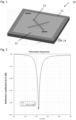
- a patch antenna 10 comprises an insulating substrate 11 and a patch element 12 arranged on one of the main surfaces of the substrate 11.
- patch element 12 may be formed directly on a PCB substrate, for example by etching a conductive copper layer arranged on an insulating layer of the PCB substrate.
- the patch element 12 has a square shape, i.e. its lengths and widths are the same. In the specific example shown in Figure 1 , its lengths and widths are 24 mm each.
- a conductive ground plane is arranged on the opposite side of the substrate 11, i.e. its backside.
- the patch element 12 is surrounded by a plurality of further, dot-shaped ground elements 14.
- a single square patch element 12 has the same polarization frequency in a vertical and horizontal direction. Thus, it may be used, for example, as a dual-polarized or circular polarized patch antenna. This can be achieved by providing respective RF signals at two separate feed points at different parts of the patch element (not shown in Figure 1 ). In case of circular polarization, a copy of the RF signal provided to the first feed point is delayed by 90° degrees in phase and provided to the second feed point.
- a slot structure 13, as shown in Figure 1 may be used to reduce the size of the patch antenna 10.
- Figure 1 also shows a coordinate system, which will be used throughout the specification. Accordingly, the height of the patch element 12 is measured in the x-direction, its width is measured in the y-direction and the thickness of the antenna 10 is measured in the z-direction of the indicated Cartesian coordinate system.
- Figure 2 shows the simulated resonance frequency for both the horizontal as well as the vertical polarization direction of the patch antenna 10 shown in Figure 1 . Due to the symmetric, square patch element 12, the two polarization frequencies coincide at a desired resonance frequency and are overlapping in Figure 2 .
- the resonance frequency is2.436 GHz. This frequency is useful, for example, for short-range RF communication, such as the WiFi technology according to IEEE 802.11 family of protocols or the Bluetooth wireless technology according to IEEE 802.15.1.
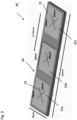
- FIG. 3 shows a patch antenna array 30 comprising three patch elements 32a, 32b and 32c arranged on a common substrate 31.
- a common ground plane (not visible in Figure 3 ) is formed, essentially covering the entire second main surface of the substrate 31. That is to say, the common ground plane forms the ground plane for all three of the patch elements 32a to 32c.
- each patch element 32a to 32c is surrounded by a plurality of further, dot-shaped ground elements
- Each of the patch elements 32a to 32c comprises a slot structure 33, as mentioned before with respect to Figure 1 .
- each of the patch elements 32a to 32c has a square shape with a common side length of, for example, 24 mm.
- the substrate 31 has a total height of 28 mm and a total width of 92 mm.
- the center points of neighboring patch elements 32b and 32c are arranged in a common row and separated in the y-direction by a center-to-center distance S of 32 mm as shown. Accordingly, two gaps 34 are formed between the first patch element 32a and second patch element 32b, and between the second patch element 32b and the third patch element 32c.
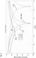
- Figure 4 shows the resulting reflection coefficient in dB depending on the operating frequency for each one of the patch elements 32a to 32c.
- the parameter S11 refers to the horizontal polarization of patch element 32b, S22 to the vertical polarization of patch element 32b, S33 to the horizontal polarization of patch element 32c, S44 to the vertical polarization of patch element 32c, S55 to the horizontal polarization of patch element 32a, and S66 to the vertical polarization of patch element 32a.
- the respective six resonance frequencies are spread over a frequency range of 2.412 GHz to 2.484 GHz, with two of them having resonance peaks m1 very close to each other at about 2.412 GHz and two further curves completely overlapping with a resonance peak m3 at 2.436 GHz. Attention is drawn to the fact that even the resonance peaks m2 and m4 of the central patch element 32b are offset from the desired resonance frequency of 2.44 GHz.
- each of dual-polarized patch antennas becomes detuned.
- the amount of detuning is different for each patch element 32 and each polarization direction, resulting in an uneven and uncontrolled behavior of the patch antenna array 30 taken as a whole.
- Figure 5 provides an alternative approach to correcting an unwanted detuning. It shows an improved patch antenna array 50 having an asymmetrical patch antenna design.
- the polarization frequencies of all patch elements 52a to 52c arranged on a common substrate 51 are controlled at a design stage. This is achieved by changing the polarization dimensions of each patch element 52a to 52c to counteract its unwanted frequency drift or detuning.
- the central patch element 52b has a width of 23.7 mm, i.e. about 1.25% less than the 24 mm edge length of the corresponding square patch element 32b, and a height of 24.8 mm, i.e. about 3.33% more than the 24 mm edge length of the corresponding square patch element 32b.
- the outer patch elements 52a and 52c each have a width of 23.7 mm and a height of 24.3 mm. That is to say, the array patch antenna is both point symmetric with respect to the center of the central patch element 52b and mirror symmetric with respect to the x- and y-axis through said central point.
- each of the three patch elements has the same width of 23.7 mm.
- an acceptable frequency windows may be defined, for example a frequency range centered at 2.440 GHz +/- 10 MHz in the presented example.
- a center-to-center distance S may lie in the range of ⁇ /4 to ⁇ /2, wherein ⁇ is the wavelength of an electromagnetic wave in air corresponding to the radio carrier frequency and the common resonance frequency.
- the center-to-center distance S typically lies around ⁇ /2, for example in a range of ⁇ /2 +/- 20% or less, preferably ⁇ /2 +/- 10% or less.
- the patch antenna array 50 also comprises a ground plane 55 running the entire board size, which is arranged on the opposite back surface of the substrate 51 and is not visible in Figure 5 .
- each of the patch elements 52 comprises a first feed point 56 and a second feed point 57 arranged in a center of each patch element 52, just left and below the central meeting point of two individual slots together forming a slot structure 53.
- These feed points 56 and 57 are connected within substrate 51, for example using internal vias of a multiplayer PCB, for connection with RF connectors at the bottom layer, which are also hidden in Figure 55.
- slot structures 53 is optional in all embodiments. It may also affect the polarization frequencies of the patch elements 52a to 52c, and may result in an overall more compact antenna design.
- the above antenna design may also be employed for patch antenna arrays with circular polarization directions, i.e. a circular-polarized antenna, and/or a single, linear polarization direction, i.e. a linear-polarized antenna.
- a circular-polarized antenna the design of the patch antenna array 50 remains essentially the same, wherein one of the signals provided to one of the two feed points 56 and 57 is 90 degrees out of phase with respect to the signal provided to the other feed point 57 or 56, respectively.
- the patch antenna array 50 with the single row of three horizontally arranged patch elements 52a to 52c as shown in Figure 5 may be configured, for example, as a vertically polarized patch antenna array.
- a single, vertical feed point 57 and/or feed signal may be provided.
- the patch antenna array 50 is configured as a horizontally polarized patch antenna array, only a single, horizontal feed point 56 or feed signal may be provided for each of the patch elements 52a to 52c.
- a single row of three horizontally arranged patch elements 52a to 52c is shown in Figure 5 , a single column of vertically arranged patch elements may also be used in either case.
- Figures 6 and 7 show results of a simulation and of actual measurements performed for the patch antenna array 50 shown in Figure 5 , respectively.
- the corresponding six polarization frequencies of each of the three patch elements 52a to 52c and each of the two polarization directions lie within a relatively narrow frequency band between 2.43 and 2.45 GHz, i.e. matches the desired frequency of 2.440 GHz +/- 10 MHz. Accordingly, no external components are required for retuning the individual patch elements 52a to 52c to the desired resonance frequency. As a result, the verification time for the entire patch antenna array 50 can be shortened considerably.
- the test time can be reduced by 80% or more due to a significant reduction of manual work required for testing.
- the proposed design is also less prone to errors as no additional components need to be connected, which may lead to further faults or tolerances.
- the omission of external components also leads to a significant reduction in costs.
- the optimization procedure can be repeated directly at the design stage, without further manual testing and retuning after manufacturing, for example, of prototypes.
- the carrier substrate 51 and thus the final patch antenna array 50 may also be smaller as compared to the solution shown in Figure 3 .
- the total width is reduced by 2 x 0.3 mm, i.e. by 0.6 mm in total.
- Figure 8 shows the steps of a method 80 for manufacturing a patch antenna array, such as the patch antenna array 50 shown in Figure 5 .
- a desired resonance frequency is determined.
- the desired resonance frequency may be determined by a specific application, such as the transmission of electromagnetic radio waves at a desired frequency determined by a corresponding standard, e.g. 2.44 GHz.
- a desired arrangement of a plurality of patch elements on a common substrate is determined.
- an one- or two-dimensional arrangement of patch elements may be determined depending on a specific transmission configuration used, for example, for AoA estimation, AoD estimation, beam forming and/or antenna diversity transmission.
- Step S20 may comprise, among others, the relative arrangement of the patch elements with respect to each other, i.e. their center-to-center distance and relative orientation of centers.
- the center-to-center distance S may be expressed as a fraction of the intended wavelength ⁇ of an RF wave to be sent or received by the patch antenna array. For example, a center-to-center distance S in the range of ⁇ /4 to ⁇ /2 may be desirable.
- other parameters, such as a material, thickness or total size of the substrate may also be defined in step S20 and taken into account in step S30 below.
- a step S30 at first an arrangement of a corresponding square patch elements is assumed and a corresponding resonance frequency for each patch element and, if applicable, polarization direction of each patch element, is determined. Thereafter, the width and/or the height of each patch element is varied until a resonance frequency for at least one, preferably all polarization directions, of each patch element corresponds to the desired resonance frequency.
- Step S30 may be further broken down, as shown in Figure 8 , into a first sub-step S31, wherein the side length of each patch element of the patch antenna array under consideration is determined, and a sequence of optimization sub-steps S32 to S35.
- each patch element may correspond to the side lengths of a single, isolated patch element 12 having a resonance frequency determined for the desired wavelength ⁇ .
- the initial edge length L may be reduced by up to 15% compared to the formula for L above.
- a rough estimation of the initial edge length L based on the wavelength may be used, followed by a computer-based optimization procedure as detailed below.
- sub-step S32 corresponding polarization frequencies are determined for each patch element.
- Sub-step S32 may be performed using computer simulations or, alternatively, using measurements on corresponding prototypes.
- a sub-step S33 it is verified whether the polarization frequencies determined in sub-step S32 fall within a desired target range, for example, a frequency band with a given bandwidth, e.g. 5, 10 or 20 MHz, and centered at the desired resonance frequency determined in step S10.
- a desired target range for example, a frequency band with a given bandwidth, e.g. 5, 10 or 20 MHz, and centered at the desired resonance frequency determined in step S10.
- step S34 the width, the length or both of one or several of the patch elements is varied in corresponding sub-steps S34 and S35, respectively.
- the process is repeated from step S32 until the verification succeeds in step S33, or, alternatively, if a predetermined number of optimization rounds have been performed.
- step S30 is completed and, in a subsequent step S40, the current configuration of the patch antenna array and each of its patch elements is output, for example, to produce a corresponding mask layer for production.
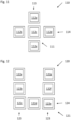
- FIGS 9 to 12 show further possible configurations of patch antenna arrays 90, 100, 110 and 120, respectively. Contrary to the one-dimensional, horizontal row of patch elements 52a to 52c shown in Figure 5 , and a corresponding vertical arrangement of patch elements in a vertical row (not shown), each one of Figures 9 to 12 shows a two-dimensional arrangement of patch elements.
- each of the patch antenna arrays 90, 100, 110 and 120 is configured similarly to the patch antenna array 50 described above.
- each of the patch antenna arrays 90, 100, 110 and 120 will contain a substrate and common ground plane.
- their respective patch elements 92, 102, 112 and 122 are configured similarly as the patch elements 52 described above.
- Figure 9 shows a matrix shape 91 of a total of nine patch elements 92a to 92i.
- the patch elements 92 are arranged in three columns 93 and three rows 94 each.
- Figure 9 shows the special case of a square 3x3 matrix.
- the patch elements 92a to 92i of the patch antenna array 90 have only four different configurations.
- the central patch element 92e has a first configuration, i.e. a specific length and height
- the four corner elements 92a, 92c, 92g and 92i have a second configuration
- the left and right patch elements 92d and 92f have a third configuration
- the remaining upper and lower patch elements 92b and 92h have a fourth configuration.
- the third and fourth configurations are similar, wherein the respective length and widths are swapped.
- the central patch element 92e will typically have a square shape, i.e. have the same length and height.
- the edge length of the square patch element patch element 92e may be above or below the average edge length of all patch elements 92a to 92i.
- Specific dimensions of the patch elements 92a to 92i are determined, for example, using the method 80 shown in Figure 8 .
- an MxN matrix shape may have M horizontal rows and N vertical columns, with M > 1 and N > 1.
- FIG. 10 shows a patch antenna array 100 having an L-shape 101.
- the L-shape 101 comprises a single column 103 and a single row 104 of three patch elements 102 each.
- the lowermost patch element 102c of the column 103 forms the leftmost patch element 102c of the row 104.
- an MxN L-shape may have one horizontal row with M patch elements and one vertical column with N patch elements joined at one of their respective ends, with M > 1 and N > 1.
- FIG. 11 shows a patch antenna array 110 with a cross shape 111. As shown therein, a single column 113 is crossing a single row 114 at their respective central patch element 112c.
- three types of patch elements exist, the central patch element 112c, the vertically extending patch elements 112a and 112e and the horizontally extending patch elements 112b and 112d. Due to the symmetry of the arrangement, the configuration of the vertically extending patch elements 112a and 112e corresponds to the configuration of the horizontal extending patch elements 112b and 112d wherein the respective length and widths are swapped. Note that in this symmetric configuration, the central patch element 112c will typically have a square shape.
- an MxN cross shape may have one horizontal row with M patch elements and one vertical column with N patch elements sharing one arbitrary patch element, preferably an inner or central patch element, with M > 1 and N > 1.
- a patch antenna array 120 with a U-shape 121 can be obtained by partially overlapping two L-shapes 101 as shown in Figure 10 .
- any two- or three-dimensional arrangement of patch antenna array is possible and envisioned by the inventors.
- each of the patch elements is arranged in a regular grid pattern.
- patch elements of one row or one column at locations corresponding to gaps of another row or column.
- a triangular overall shape of the patch antenna array may be obtained (not shown). The more complex the relative arrangement, the more useful it becomes to determine and verify the configuration of each patch element using computer simulations.
Landscapes
- Engineering & Computer Science (AREA)
- Manufacturing & Machinery (AREA)
- Waveguide Aerials (AREA)
- Variable-Direction Aerials And Aerial Arrays (AREA)
Priority Applications (3)
| Application Number | Priority Date | Filing Date | Title |
|---|---|---|---|
| EP23163659.8A EP4435973A1 (fr) | 2023-03-23 | 2023-03-23 | Réseau d'antennes à plaque et procédé de fabrication d'un réseau d'antennes à plaque |
| US18/602,529 US20240322450A1 (en) | 2023-03-23 | 2024-03-12 | Patch antenna array and method for manufacturing a patch antenna array |
| CN202410334331.2A CN118693536A (zh) | 2023-03-23 | 2024-03-22 | 贴片天线阵列和用于制造贴片天线阵列的方法 |
Applications Claiming Priority (1)
| Application Number | Priority Date | Filing Date | Title |
|---|---|---|---|
| EP23163659.8A EP4435973A1 (fr) | 2023-03-23 | 2023-03-23 | Réseau d'antennes à plaque et procédé de fabrication d'un réseau d'antennes à plaque |
Publications (1)
| Publication Number | Publication Date |
|---|---|
| EP4435973A1 true EP4435973A1 (fr) | 2024-09-25 |
Family
ID=85726573
Family Applications (1)
| Application Number | Title | Priority Date | Filing Date |
|---|---|---|---|
| EP23163659.8A Pending EP4435973A1 (fr) | 2023-03-23 | 2023-03-23 | Réseau d'antennes à plaque et procédé de fabrication d'un réseau d'antennes à plaque |
Country Status (3)
| Country | Link |
|---|---|
| US (1) | US20240322450A1 (fr) |
| EP (1) | EP4435973A1 (fr) |
| CN (1) | CN118693536A (fr) |
Citations (3)
| Publication number | Priority date | Publication date | Assignee | Title |
|---|---|---|---|---|
| CN110112577A (zh) * | 2019-05-20 | 2019-08-09 | 电子科技大学 | 一种应用于5g通信的紧凑双极化大规模mimo天线 |
| US20200303833A1 (en) * | 2017-12-12 | 2020-09-24 | Murata Manufacturing Co., Ltd. | Radio frequency module and communication device |
| US20220094075A1 (en) * | 2020-09-22 | 2022-03-24 | Qualcomm Incorporated | Dual-feed dual-band interleaved antenna configuration |
Family Cites Families (5)
| Publication number | Priority date | Publication date | Assignee | Title |
|---|---|---|---|---|
| FR2691015B1 (fr) * | 1992-05-05 | 1994-10-07 | Aerospatiale | Antenne-réseau de type micro-ruban à faible épaisseur mais à large bande passante. |
| US7268687B2 (en) * | 2004-03-23 | 2007-09-11 | 3M Innovative Properties Company | Radio frequency identification tags with compensating elements |
| JP5427226B2 (ja) * | 2011-12-08 | 2014-02-26 | 電気興業株式会社 | 送受信分離偏波共用アンテナ |
| JP6742397B2 (ja) * | 2016-03-04 | 2020-08-19 | 株式会社村田製作所 | アレーアンテナ |
| EP3819985B1 (fr) * | 2019-11-08 | 2024-04-24 | Carrier Corporation | Antenne planaire à microruban ayant une largeur de bande accrue |
-
2023
- 2023-03-23 EP EP23163659.8A patent/EP4435973A1/fr active Pending
-
2024
- 2024-03-12 US US18/602,529 patent/US20240322450A1/en active Pending
- 2024-03-22 CN CN202410334331.2A patent/CN118693536A/zh active Pending
Patent Citations (3)
| Publication number | Priority date | Publication date | Assignee | Title |
|---|---|---|---|---|
| US20200303833A1 (en) * | 2017-12-12 | 2020-09-24 | Murata Manufacturing Co., Ltd. | Radio frequency module and communication device |
| CN110112577A (zh) * | 2019-05-20 | 2019-08-09 | 电子科技大学 | 一种应用于5g通信的紧凑双极化大规模mimo天线 |
| US20220094075A1 (en) * | 2020-09-22 | 2022-03-24 | Qualcomm Incorporated | Dual-feed dual-band interleaved antenna configuration |
Non-Patent Citations (2)
| Title |
|---|
| CHEN HUNG-CHEN ET AL: "Design of Series-Fed Bandwidth-Enhanced Microstrip Antenna Array for Millimetre-Wave Beamforming Applications", INTERNATIONAL JOURNAL OF ANTENNAS AND PROPAGATION, vol. 2019, 3 June 2019 (2019-06-03), pages 1 - 10, XP055772887, ISSN: 1687-5869, Retrieved from the Internet <URL:http://downloads.hindawi.com/journals/ijap/2019/3857964.xml> DOI: 10.1155/2019/3857964 * |
| GOH CHIN HOCK ET AL: "Design of patch antennas array at low frequency application by using unknown FR4 material", CONTROL SYSTEM, COMPUTING AND ENGINEERING (ICCSCE), 2011 IEEE INTERNATIONAL CONFERENCE ON, IEEE, 25 November 2011 (2011-11-25), pages 302 - 305, XP032171791, ISBN: 978-1-4577-1640-9, DOI: 10.1109/ICCSCE.2011.6190541 * |
Also Published As
| Publication number | Publication date |
|---|---|
| US20240322450A1 (en) | 2024-09-26 |
| CN118693536A (zh) | 2024-09-24 |
Similar Documents
| Publication | Publication Date | Title |
|---|---|---|
| KR102063222B1 (ko) | 안테나 어레이에서의 상호 결합을 감소시키기 위한 장치 및 방법 | |
| US9812786B2 (en) | Metamaterial-based transmitarray for multi-beam antenna array assemblies | |
| US6320544B1 (en) | Method of producing desired beam widths for antennas and antenna arrays in single or dual polarization | |
| US9323877B2 (en) | Beam-steered wide bandwidth electromagnetic band gap antenna | |
| EP3025392B1 (fr) | Antenne à bande électromagnétique interdite dépendant de la polarisation et procédés associés | |
| US20100117916A1 (en) | Polarization dependent beamwidth adjuster | |
| US9831566B2 (en) | Radiating element for an active array antenna consisting of elementary tiles | |
| WO2015006314A2 (fr) | Antennes | |
| US20130285865A1 (en) | Printed slot-type directional antenna, and system comprising an array of a plurality of printed slot-type directional antennas | |
| JP2018074240A (ja) | アンテナ装置 | |
| WO2013031518A1 (fr) | Antenne planaire en f inversé | |
| EP1730810B1 (fr) | Antenne a gain eleve pour frequences micro-ondes | |
| WO2002023669A1 (fr) | Antenne double polarisee | |
| EP4435973A1 (fr) | Réseau d'antennes à plaque et procédé de fabrication d'un réseau d'antennes à plaque | |
| Bakr et al. | Compact broadband frequency selective microstrip antenna and its application to indoor positioning systems for wireless networks | |
| US10980107B2 (en) | Electromagnetic blocking structure, dielectric substrate, and unit cell | |
| US20060170596A1 (en) | High gain antenna for microwave frequencies | |
| JP6464124B2 (ja) | アンテナ装置 | |
| TW202501883A (zh) | 雙極化貼片式天線 | |
| Rowe et al. | 3D frequency selective surfaces with highly selective reponses | |
| JP3215295U (ja) | 立体アンテナ | |
| WO2022138477A1 (fr) | Appareil de communication sans fil | |
| EP4550579A1 (fr) | Élément d'antenne, substrat d'antenne et module d'antenne | |
| US20250337174A1 (en) | Two-dimensional microstrip patch antennas and arrays with radiation pattern decoupling | |
| CN224053403U (zh) | 圆极化天线 |
Legal Events
| Date | Code | Title | Description |
|---|---|---|---|
| PUAI | Public reference made under article 153(3) epc to a published international application that has entered the european phase |
Free format text: ORIGINAL CODE: 0009012 |
|
| STAA | Information on the status of an ep patent application or granted ep patent |
Free format text: STATUS: THE APPLICATION HAS BEEN PUBLISHED |
|
| AK | Designated contracting states |
Kind code of ref document: A1 Designated state(s): AL AT BE BG CH CY CZ DE DK EE ES FI FR GB GR HR HU IE IS IT LI LT LU LV MC ME MK MT NL NO PL PT RO RS SE SI SK SM TR |
|
| STAA | Information on the status of an ep patent application or granted ep patent |
Free format text: STATUS: REQUEST FOR EXAMINATION WAS MADE |
|
| 17P | Request for examination filed |
Effective date: 20250324 |