EP4439896A1 - Commande d'un composant semi-conducteur d'un limiteur de courant - Google Patents
Commande d'un composant semi-conducteur d'un limiteur de courant Download PDFInfo
- Publication number
- EP4439896A1 EP4439896A1 EP23166019.2A EP23166019A EP4439896A1 EP 4439896 A1 EP4439896 A1 EP 4439896A1 EP 23166019 A EP23166019 A EP 23166019A EP 4439896 A1 EP4439896 A1 EP 4439896A1
- Authority
- EP
- European Patent Office
- Prior art keywords
- semiconductor component
- controllable semiconductor
- control unit
- electric current
- current limiter
- Prior art date
- Legal status (The legal status is an assumption and is not a legal conclusion. Google has not performed a legal analysis and makes no representation as to the accuracy of the status listed.)
- Withdrawn
Links
Images


Classifications
-
- H—ELECTRICITY
- H02—GENERATION; CONVERSION OR DISTRIBUTION OF ELECTRIC POWER
- H02H—EMERGENCY PROTECTIVE CIRCUIT ARRANGEMENTS
- H02H9/00—Emergency protective circuit arrangements for limiting excess current or voltage without disconnection
- H02H9/02—Emergency protective circuit arrangements for limiting excess current or voltage without disconnection responsive to excess current
- H02H9/025—Current limitation using field effect transistors
-
- H—ELECTRICITY
- H02—GENERATION; CONVERSION OR DISTRIBUTION OF ELECTRIC POWER
- H02H—EMERGENCY PROTECTIVE CIRCUIT ARRANGEMENTS
- H02H3/00—Emergency protective circuit arrangements for automatic disconnection directly responsive to an undesired change from normal electric working condition with or without subsequent reconnection ; integrated protection
- H02H3/02—Details
- H02H3/04—Details with warning or supervision in addition to disconnection, e.g. for indicating that protective apparatus has functioned
- H02H3/042—Details with warning or supervision in addition to disconnection, e.g. for indicating that protective apparatus has functioned combined with means for locating the fault
-
- H—ELECTRICITY
- H02—GENERATION; CONVERSION OR DISTRIBUTION OF ELECTRIC POWER
- H02H—EMERGENCY PROTECTIVE CIRCUIT ARRANGEMENTS
- H02H7/00—Emergency protective circuit arrangements specially adapted for specific types of electric machines or apparatus or for sectionalised protection of cable or line systems, and effecting automatic switching in the event of an undesired change from normal working conditions
- H02H7/008—Emergency protective circuit arrangements specially adapted for specific types of electric machines or apparatus or for sectionalised protection of cable or line systems, and effecting automatic switching in the event of an undesired change from normal working conditions for protective arrangements according to this subclass
-
- H—ELECTRICITY
- H03—ELECTRONIC CIRCUITRY
- H03K—PULSE TECHNIQUE
- H03K17/00—Electronic switching or gating, i.e. not by contact-making and –breaking
- H03K17/08—Modifications for protecting switching circuit against overcurrent or overvoltage
- H03K17/082—Modifications for protecting switching circuit against overcurrent or overvoltage by feedback from the output to the control circuit
- H03K17/0822—Modifications for protecting switching circuit against overcurrent or overvoltage by feedback from the output to the control circuit in field-effect transistor switches
-
- H—ELECTRICITY
- H02—GENERATION; CONVERSION OR DISTRIBUTION OF ELECTRIC POWER
- H02H—EMERGENCY PROTECTIVE CIRCUIT ARRANGEMENTS
- H02H3/00—Emergency protective circuit arrangements for automatic disconnection directly responsive to an undesired change from normal electric working condition with or without subsequent reconnection ; integrated protection
- H02H3/02—Details
- H02H3/025—Disconnection after limiting, e.g. when limiting is not sufficient or for facilitating disconnection
-
- H—ELECTRICITY
- H02—GENERATION; CONVERSION OR DISTRIBUTION OF ELECTRIC POWER
- H02H—EMERGENCY PROTECTIVE CIRCUIT ARRANGEMENTS
- H02H3/00—Emergency protective circuit arrangements for automatic disconnection directly responsive to an undesired change from normal electric working condition with or without subsequent reconnection ; integrated protection
- H02H3/02—Details
- H02H3/06—Details with automatic reconnection
-
- H—ELECTRICITY
- H03—ELECTRONIC CIRCUITRY
- H03K—PULSE TECHNIQUE
- H03K17/00—Electronic switching or gating, i.e. not by contact-making and –breaking
- H03K17/08—Modifications for protecting switching circuit against overcurrent or overvoltage
- H03K2017/0806—Modifications for protecting switching circuit against overcurrent or overvoltage against excessive temperature
Definitions
- the present invention relates to a method for controlling a semiconductor component of an electric current limiter circuit of a power supply.
- the present invention further relates to a control unit for executing the method, a computer program product, and to a corresponding electric circuit.
- Protection circuits such as electric current limiters are employed to limit an electric current that is delivered to a load so that the power supply is protected in case of short circuit or other overloads.
- the limiting element of electric current limiters may be exposed to high currents which may risk overheating.
- Electric current limiters and their limiting elements typically includes custom made and designed circuits for the specific load case and often include expensive integrated circuits.
- a method for controlling a semiconductor component of an electric current limiter circuit for a power supply, the controllable semiconductor component to be connected to a load at the output of the current limiter circuit as a current limiting component comprises: sampling, by a control unit, measurements of a voltage across the controllable semiconductor component or across the current limiter at a sampling frequency, calculating, by the control unit, an energy dissipated in the controllable semiconductor component during a time duration based on the sampled voltage and an electric current value, and controlling, by the control unit, the controllable semiconductor component to allow for recovery time durations to maintain a temperature of the controllable semiconductor component below a predetermined limit.
- the present invention is at least partly based on the realization to actively control the semiconductor component with recovery time durations so that the temperature, or dissipated energy, in the semiconductor component is kept sufficiently low and within thermal specifications.
- the energy dissipated in the semiconductor component is continuously, with a sampling rate, calculated so that the semiconductor component can be timely disconnected from the load to allow for recovery so that the average dissipated energy over a cycle is kept low.
- To be kept low is interpreted such that the temperature of the semiconductor component is below the predetermined limit which may be given by thermal specifications of the semiconductor component.
- the voltage measurement that is sampled may be measured across be across the semiconductor component. Alternatively, the voltage measurement that is sampled may be measured across the electric current limiter.
- the method may be implemented using firmware running on a control unit controlling the hardware semiconductor component. This control may be implemented in a wide range of loads and protection circuits.
- controlling the controllable semiconductor component may comprise switching off, by the control unit, the controllable semiconductor component for a recovery time duration. That is, for a given recovery time duration, the semiconductor component does not allow the transfer electric current from the power supply to the load. Thereby, no, or very little, energy is dissipated in the semiconductor component.
- controlling the controllable semiconductor component may comprise switching on, by the control unit, the controllable semiconductor component once the recovery time duration has lapsed.
- the semiconductor component is switched back on to proceed operation and transfer of electric current to the load. Switching on and off the semiconductor component may be continuously performed with a duty cycle.
- the method may comprise monitoring the calculated dissipated energy, and when the calculated dissipated energy exceeds a threshold, controlling the semiconductor component to allow for a recovery time duration.
- the dissipated energy is relatively straight forward to calculate as the time integral of dissipated power given by the product of electric current and voltage and thus provides for a convenient measure to determine when to allow the semiconductor component to recover
- the threshold with which the calculated dissipated energy is compared may be adjustable by the control unit.
- the threshold may be adapted to better fit environmental circumstances, ambient temperature, load cases, etc.
- the method may comprise determining a voltage drop across the current limiter, and when the voltage drop exceeds an allowed voltage limit, calculating, the energy dissipated and controlling the controllable semiconductor component. That is, the method may be initiated once the voltage drop exceeds the limit which may indicate an electric fault such as a short circuit or overload.
- the recovery time duration is such that a duty cycle of the controllable semiconductor component is less than 10%, or less than or equal to 5%.
- the duty cycle is calculated to make sure that the average dissipated energy over a time window, i.e., one period of the operation of the semiconductor component, is below the threshold which is adapted to ensure that the semiconductor component does not overheat. For example, if the semiconductor component is operating at the electric current limit of the electric current limiter, the semiconductor component may be allowed to be on for a time duration until the semiconductor component is given a recovery time duration.
- the recovery time duration may be in the range of about 10-1000 times the time duration at the electric current limit, such as at least 10 times the time duration at the electric current limit, or 20 times time duration at the electric current limit, or even or 40 times time duration at the electric current limit. In some possible embodiments, the recovery time duration may be up to 500 times the time duration at the electric current limit or even 1000 times the time duration at the electric current limit.
- the electric current value may be a predetermined value.
- the predetermined electric current value may for example be a rated maximum current of the electric current limiter.
- the method may comprise sampling measurements of an electric current through the semiconductor component to obtain electric current values. That is, the electric current value may be a measured electric current.
- the controllable semiconductor component may be a transistor.
- the transistor may be of various kinds such as a field effect transistor (FET), metal-oxide-semiconductor field-effect transistor (MOSFET), junction field effect transistor (JFET), and bipolar junction transistor (BJT).
- FET field effect transistor
- MOSFET metal-oxide-semiconductor field-effect transistor
- JFET junction field effect transistor
- BJT bipolar junction transistor
- the current limiter may be configured for a maximum electric current in the range of about 50 mA to about 5 A, such as for example about 5 A, about 3 A, preferably about 1 A, more preferably about 700 mA, more preferably less about 100 mA, or about 50 mA, to be supplied to the load.
- Sampling and calculating the dissipated energy may be performed at a rate within a range of 100 Hz - 5 kHz, such as a 1 kHz repetition rate.
- an electric circuit comprising: a power supply input for receiving electric power to be delivered to a load; a current limiter electrically connected between the power supply and the load, the current limiter comprises a controllable semiconductor component connectable to the load as a current limiting component; a control unit configured to: sample measurements of a voltage across the controllable semiconductor component at a sampling frequency, calculate an energy dissipated in the controllable semiconductor component during a time duration based on the sampled voltage and an electric current value, and control the controllable semiconductor component to allow for recovery time durations to maintain a temperature of the controllable semiconductor component below a predetermined limit.
- controllable semiconductor component may be a transistor.
- a computer program product comprising a non-transitory computer readable medium having stored thereon computer program means for executing the method.
- The is further provided a control unit configured to execute the method.
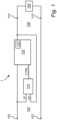
- Fig. 1 illustrates an electric circuit 1 according to one embodiment.
- the electric circuit comprises a power supply input 101 for receiving electric power to be delivered to a load.
- the input is connectable to a power supply via suitable electrical connection ports 102.
- the electric circuit 1 comprises a current limiter 104 electrically connected between the power supply input 101 and a load 106 connected to the output 108 at electrical ports 110.
- the current limiter 104 comprises a controllable semiconductor component 112 connectable to the load 106 as an electric current limiting component.
- the electric current limiter 104 is configured to limit an electric current that is delivered to the load 106 so that the power supply at the input 101 is protected in case of short circuit or other overloads or faults.
- the electric circuit 1 comprises a control unit 114, such as a microcontroller that can receive voltage measurements, Ui, Uo, from sensors of the circuit 1, but also provide control signals CTRL to the current limiter 104 to for example control the operation of the semiconductor element 112.
- a control unit 114 such as a microcontroller that can receive voltage measurements, Ui, Uo, from sensors of the circuit 1, but also provide control signals CTRL to the current limiter 104 to for example control the operation of the semiconductor element 112.
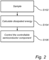
- the control unit 114 is configured to sample, in step S102, measurements of a voltage, Ui-Uo, across the controllable semiconductor component and/or across the electric current limiter 104 at a sampling frequency.
- the sampling frequency may be in the range of 100 Hz to about 5 kHz, such as at about 1 kHz.
- step S104 calculate, by the control unit 114, an energy dissipated in the controllable semiconductor component 112 during a time duration based on the sampled voltage and an electric current value.
- the electric current value is a predetermined value set by an electric current rating of the electric current limiter 104.
- the predetermined electric current value may be 50 mA, 100mA, 500mA, 1A, 3A, 3.3A, 4A, 5A, to mention some examples. It is also envisaged that the electric current value may be a sampled measurement of an electric current through the semiconductor component.
- step S106 controlling, by the control unit 114 by transmitting the control signals CTRL, the controllable semiconductor component 112 to allow for recovery time durations to maintain a temperature of the controllable semiconductor component 112 below a predetermined limit.
- the predetermined limit may be according to thermal specifications of the controllable semiconductor component 112.
- Controlling the controllable semiconductor component may comprise switching off, by the control unit 114, the controllable semiconductor component 310 for a recovery time duration by setting the CTRL signal to OFF.
- control unit 114 may switch on by setting the CTRL signal to ON, the controllable semiconductor component 310 once the recovery time duration has lapsed.
- Fig. 3 is a block diagram of an electric circuit 3 according to an example embodiment.
- the electric circuit 3 comprises the input port 101, the output port 108, the control unit 114 as described above.
- the electric current limiter 304 comprises a sensing resistor 306, a regulating circuit 308, and a controllable semiconductor component in the form of a transistor 310.
- the gate 312 of the transistor 310 is connected to an output port 314 of the regulating circuit 308.
- Inputs 316a-b of the regulating circuit 308 are connected across the sensing resistor 306.
- the regulating circuit 308 is configured to sense a voltage across the sensing resistor 306 and to accordingly control the transistor via its gate 312 to limit the electric current through the transistor 310 according to a maximum allowed electric current.
- the regulating circuit 308 may be provided in various forms and comprise electrical components including operational amplifiers or bipolar transistors, and other components for regulating the transistor current.
- the regulating circuit 308 When the regulating circuit 308 receives OFF, the transistor 310 is switched off and does not allow electric current to pass to the output 108.
- the control signal CTRL may be considered an enable-disable signal that overrides the normal function of the regulating circuit 308.
- circuit 3 is a schematic drawing and may comprise additional electrical components.
- an energy dissipation parameter E is set to zero in step S101.
- step S102 the control unit 114 samples a voltage drop (Ui-Uo) across the electric current limiter 304. If the control unit 114 determines, in step S103 that the voltage drop exceeds an allowed voltage limit and the CTRL signal is presently set to ON, that is, the transistor 310 is powered on and operative, e.g., switched on, the dissipated energy is calculated in step S104 as the product between the voltage drop Ui-Uo and the electric current value I.
- the allowed voltage limit is such that it exceeds the voltage drop under normal operation with a set margin. If a fault is detected, such as a short circuit in the load, the voltage drop (Ui-Uo) across the electric current limiter 304 increases so that it exceeds the allowed voltage limit.
- the calculated dissipated energy (Ui-Uo)*I in step S104 is added to the energy dissipation parameter Ek.
- the calculated energy from each iteration is accumulated in the energy dissipation parameter E.
- the control unit 114 determines that the accumulated dissipated energy, that is, the present energy parameter Ek exceeds an energy threshold E Max in step S105, the control unit 114 controls the semiconductor component 310 to allow for a recovery time duration. For this, the control unit 114 sets the control signal CTRL to OFF, i.e., a low signal in step S106a. The method returns to step S102.
- step S105 If the accumulated dissipated energy, that is, the present energy parameter Ek does not exceed the energy threshold E Max in step S105, a new sample is acquired in step S102. Assuming that the voltage drop is still above the allowed limit, a further calculation of dissipated energy is performed in step S104, and the present accumulated dissipated energy parameter E is again compared with the energy threshold E Max in step S105. As discussed above, once a present accumulated energy parameter Ek exceeds the energy threshold E Max in step S105, the control signal CTRL is set to OFF in the control step S106a, comprising to switch off the transistor 310.
- step S108 if the outcome is negative in subsequent step S103, e.g. since the control signal CTRL is set to OFF, the energy dissipation parameter Ek representing the accumulated dissipated energy is compared with zero in step S108.
- the recovery energy amount E Recovery may be determined from empirical or theoretical calculations.
- step S108 the control unit 114 controls the transistor 310 in step S106b.
- step S106b the control unit 114 switches on the transistor 310 by setting the control signal to ON, that is, by providing a high signal.
- the energy dissipation parameter E is reset at zero, thus, the method returns to step S101.
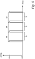
- Fig. 5 illustrates a control signal CTRL as a function of time to illustrate that the control of the transistor 310 may be periodically performed.
- the recovery time duration Tr is preferably such that the duty cycle is less than 10%, or less than or equal to 5%.
- the recovery time duration Tr is at least 90% of a period time Pt of the controllable semiconductor component 310.
- the recovery time duration Tr may be calculated as a factor multiplied by the time duration which the transistor is allowed to operate at its electric current limit, e.g. when the CTRL indicates ON and the operation is at the rated maximum power or electric current of the semiconductor component. Such factor may be in the range 10-1000, such as 20, 30, 40, 500, or even 1000.
- the recovery time duration, or duration, Tr is adapted so that the average energy dissipated over one period time Pt is sufficiently low to not cause overheating of the transistor 310.
- the CTRL signal indicated OFF.
- a computer program product comprising a computer readable medium having stored thereon computer program means for executing the method according to any one or the herein described embodiments.
- the non-transitory computer readable medium is preferably accessible by the control unit 114, provided as a microcontroller or microprocessor.
- a control unit may include a microprocessor, microcontroller, programmable digital signal processor or another programmable device.
- the control unit may also, or instead, include an application specific integrated circuit, a programmable gate array or programmable array logic, a programmable logic device, or a digital signal processor.
- the control unit includes a programmable device such as the microprocessor, microcontroller or programmable digital signal processor mentioned above, the processor may further include computer executable code that controls operation of the programmable device.
- Computer-readable media may include computer-readable storage media, which correspond to tangible media such as data storage media, or communication media including any media that facilitate the transfer of a computer program from one place to another, e.g., according to a communication protocol.
- Computer-readable media generally may correspond to (1) tangible computer-readable storage media which are non-transitory or (2) a communication media such as signal or carrier waves.
- Data storage media may be any available media that can be accessed by one or more computers or one or more processors to retrieve instructions, code and/or data structures for implementation of the techniques described in this disclosure.
- a computer program product may include a computer-readable medium.
- such computer-readable storage media can comprise RAM, ROM, EEPROM, CD-ROM or other optical disk storage, magnetic disk storage, or other magnetic storage devices, flash memory, or any other medium that can be used to store desired program code in the form of instructions or data structures and that can be accessed by a computer.
Landscapes
- Engineering & Computer Science (AREA)
- Power Engineering (AREA)
- Electronic Switches (AREA)
Priority Applications (1)
| Application Number | Priority Date | Filing Date | Title |
|---|---|---|---|
| EP23166019.2A EP4439896A1 (fr) | 2023-03-31 | 2023-03-31 | Commande d'un composant semi-conducteur d'un limiteur de courant |
Applications Claiming Priority (1)
| Application Number | Priority Date | Filing Date | Title |
|---|---|---|---|
| EP23166019.2A EP4439896A1 (fr) | 2023-03-31 | 2023-03-31 | Commande d'un composant semi-conducteur d'un limiteur de courant |
Publications (1)
| Publication Number | Publication Date |
|---|---|
| EP4439896A1 true EP4439896A1 (fr) | 2024-10-02 |
Family
ID=85800247
Family Applications (1)
| Application Number | Title | Priority Date | Filing Date |
|---|---|---|---|
| EP23166019.2A Withdrawn EP4439896A1 (fr) | 2023-03-31 | 2023-03-31 | Commande d'un composant semi-conducteur d'un limiteur de courant |
Country Status (1)
| Country | Link |
|---|---|
| EP (1) | EP4439896A1 (fr) |
Citations (4)
| Publication number | Priority date | Publication date | Assignee | Title |
|---|---|---|---|---|
| DE20010283U1 (de) * | 2000-06-08 | 2001-07-19 | Siemens AG, 80333 München | Stromversorgung mit verlustarmer Einschaltstrombegrenzung |
| US8299767B1 (en) * | 2006-08-18 | 2012-10-30 | Picor Corporation | Dynamic safe operating area control |
| WO2019145017A1 (fr) * | 2018-01-23 | 2019-08-01 | Renesas Electronics Corporation | Circuit de protection contre la surchauffe |
| EP3998686A1 (fr) * | 2021-02-19 | 2022-05-18 | Lilium eAircraft GmbH | Controlleur de puissance à l'état solide |
-
2023
- 2023-03-31 EP EP23166019.2A patent/EP4439896A1/fr not_active Withdrawn
Patent Citations (4)
| Publication number | Priority date | Publication date | Assignee | Title |
|---|---|---|---|---|
| DE20010283U1 (de) * | 2000-06-08 | 2001-07-19 | Siemens AG, 80333 München | Stromversorgung mit verlustarmer Einschaltstrombegrenzung |
| US8299767B1 (en) * | 2006-08-18 | 2012-10-30 | Picor Corporation | Dynamic safe operating area control |
| WO2019145017A1 (fr) * | 2018-01-23 | 2019-08-01 | Renesas Electronics Corporation | Circuit de protection contre la surchauffe |
| EP3998686A1 (fr) * | 2021-02-19 | 2022-05-18 | Lilium eAircraft GmbH | Controlleur de puissance à l'état solide |
Similar Documents
| Publication | Publication Date | Title |
|---|---|---|
| US9966943B2 (en) | System and method for a high-side power switch | |
| US12484203B2 (en) | Systems and methods for controlled active discharge for inverter for electric vehicle | |
| US7940034B2 (en) | Apparatus for detecting a state of operation of a power semiconductor device | |
| CN107276572B (zh) | 具有测试模式功能的电子开关和保护电路 | |
| US8598859B2 (en) | Power supply controller | |
| US8270138B2 (en) | Power supply controller and threshold adjustment method thereof | |
| CN101652927B (zh) | 用于负载电路的过电流保护装置 | |
| JP5639868B2 (ja) | 負荷回路の保護装置 | |
| CA3000877C (fr) | Disjoncteur electronique | |
| US8488289B2 (en) | Current protection circuit for intelligent power switch | |
| EP0525255A1 (fr) | Circuit de protection pour dispositif semi-conducteur | |
| US20140247523A1 (en) | Switching regulator and electronic device | |
| US11133667B2 (en) | Protection circuit, corresponding system and method | |
| US10355474B2 (en) | Inrush current prevention circuit, inrush current prevention method, and computer readable medium | |
| CN107408884B (zh) | 电力转换装置及电力转换装置的控制方法 | |
| US7710700B2 (en) | DC/DC converter with current limit protection | |
| US10585131B2 (en) | In-vehicle determination circuit and in-vehicle power supply device | |
| CN111464029A (zh) | 用于dc-dc转换器的电流感测控制器 | |
| US10809777B2 (en) | Energy estimation for thermal management | |
| EP4439896A1 (fr) | Commande d'un composant semi-conducteur d'un limiteur de courant | |
| US11418021B2 (en) | Device circuit breaker having intelligent limit value determination and method therefor | |
| CN104283199A (zh) | 采用多开关的涌入控制 | |
| JPH0533071Y2 (fr) | ||
| EP3515744B1 (fr) | Protection thermique basée sur une minuterie pour composants de puissance d'une alimentation à découpage | |
| JPH07221261A (ja) | 温度センサを有する電力用半導体デバイス |
Legal Events
| Date | Code | Title | Description |
|---|---|---|---|
| PUAI | Public reference made under article 153(3) epc to a published international application that has entered the european phase |
Free format text: ORIGINAL CODE: 0009012 |
|
| STAA | Information on the status of an ep patent application or granted ep patent |
Free format text: STATUS: THE APPLICATION HAS BEEN PUBLISHED |
|
| AK | Designated contracting states |
Kind code of ref document: A1 Designated state(s): AL AT BE BG CH CY CZ DE DK EE ES FI FR GB GR HR HU IE IS IT LI LT LU LV MC ME MK MT NL NO PL PT RO RS SE SI SK SM TR |
|
| STAA | Information on the status of an ep patent application or granted ep patent |
Free format text: STATUS: THE APPLICATION IS DEEMED TO BE WITHDRAWN |
|
| 18D | Application deemed to be withdrawn |
Effective date: 20250403 |