EP4447079A1 - Kondensatorkomponente und herstellungsverfahren dafür sowie elektronische vorrichtung - Google Patents
Kondensatorkomponente und herstellungsverfahren dafür sowie elektronische vorrichtung Download PDFInfo
- Publication number
- EP4447079A1 EP4447079A1 EP24163564.8A EP24163564A EP4447079A1 EP 4447079 A1 EP4447079 A1 EP 4447079A1 EP 24163564 A EP24163564 A EP 24163564A EP 4447079 A1 EP4447079 A1 EP 4447079A1
- Authority
- EP
- European Patent Office
- Prior art keywords
- layer
- trace
- connection pad
- electrode layer
- trench
- Prior art date
- Legal status (The legal status is an assumption and is not a legal conclusion. Google has not performed a legal analysis and makes no representation as to the accuracy of the status listed.)
- Pending
Links
Images


Classifications
-
- H—ELECTRICITY
- H01—ELECTRIC ELEMENTS
- H01G—CAPACITORS; CAPACITORS, RECTIFIERS, DETECTORS, SWITCHING DEVICES, LIGHT-SENSITIVE OR TEMPERATURE-SENSITIVE DEVICES OF THE ELECTROLYTIC TYPE
- H01G4/00—Fixed capacitors; Processes of their manufacture
- H01G4/33—Thin- or thick-film capacitors (thin- or thick-film circuits; capacitors without a potential-jump or surface barrier specially adapted for integrated circuits, details thereof, multistep manufacturing processes therefor)
-
- H—ELECTRICITY
- H10—SEMICONDUCTOR DEVICES; ELECTRIC SOLID-STATE DEVICES NOT OTHERWISE PROVIDED FOR
- H10W—GENERIC PACKAGES, INTERCONNECTIONS, CONNECTORS OR OTHER CONSTRUCTIONAL DETAILS OF DEVICES COVERED BY CLASS H10
- H10W20/00—Interconnections in chips, wafers or substrates
- H10W20/40—Interconnections external to wafers or substrates, e.g. back-end-of-line [BEOL] metallisations or vias connecting to gate electrodes
- H10W20/495—Capacitive arrangements or effects of, or between wiring layers
- H10W20/496—Capacitor integral with wiring layers
-
- H—ELECTRICITY
- H01—ELECTRIC ELEMENTS
- H01G—CAPACITORS; CAPACITORS, RECTIFIERS, DETECTORS, SWITCHING DEVICES, LIGHT-SENSITIVE OR TEMPERATURE-SENSITIVE DEVICES OF THE ELECTROLYTIC TYPE
- H01G4/00—Fixed capacitors; Processes of their manufacture
- H01G4/002—Details
- H01G4/005—Electrodes
- H01G4/012—Form of non-self-supporting electrodes
-
- H—ELECTRICITY
- H10—SEMICONDUCTOR DEVICES; ELECTRIC SOLID-STATE DEVICES NOT OTHERWISE PROVIDED FOR
- H10D—INORGANIC ELECTRIC SEMICONDUCTOR DEVICES
- H10D1/00—Resistors, capacitors or inductors
- H10D1/01—Manufacture or treatment
- H10D1/041—Manufacture or treatment of capacitors having no potential barriers
- H10D1/042—Manufacture or treatment of capacitors having no potential barriers using deposition processes to form electrode extensions
-
- H—ELECTRICITY
- H10—SEMICONDUCTOR DEVICES; ELECTRIC SOLID-STATE DEVICES NOT OTHERWISE PROVIDED FOR
- H10D—INORGANIC ELECTRIC SEMICONDUCTOR DEVICES
- H10D1/00—Resistors, capacitors or inductors
- H10D1/60—Capacitors
- H10D1/68—Capacitors having no potential barriers
- H10D1/692—Electrodes
- H10D1/711—Electrodes having non-planar surfaces, e.g. formed by texturisation
- H10D1/716—Electrodes having non-planar surfaces, e.g. formed by texturisation having vertical extensions
-
- H—ELECTRICITY
- H10—SEMICONDUCTOR DEVICES; ELECTRIC SOLID-STATE DEVICES NOT OTHERWISE PROVIDED FOR
- H10W—GENERIC PACKAGES, INTERCONNECTIONS, CONNECTORS OR OTHER CONSTRUCTIONAL DETAILS OF DEVICES COVERED BY CLASS H10
- H10W20/00—Interconnections in chips, wafers or substrates
- H10W20/01—Manufacture or treatment
- H10W20/031—Manufacture or treatment of conductive parts of the interconnections
-
- H—ELECTRICITY
- H10—SEMICONDUCTOR DEVICES; ELECTRIC SOLID-STATE DEVICES NOT OTHERWISE PROVIDED FOR
- H10W—GENERIC PACKAGES, INTERCONNECTIONS, CONNECTORS OR OTHER CONSTRUCTIONAL DETAILS OF DEVICES COVERED BY CLASS H10
- H10W20/00—Interconnections in chips, wafers or substrates
- H10W20/01—Manufacture or treatment
- H10W20/031—Manufacture or treatment of conductive parts of the interconnections
- H10W20/032—Manufacture or treatment of conductive parts of the interconnections of conductive barrier, adhesion or liner layers
- H10W20/038—Manufacture or treatment of conductive parts of the interconnections of conductive barrier, adhesion or liner layers covering conductive structures
-
- H—ELECTRICITY
- H10—SEMICONDUCTOR DEVICES; ELECTRIC SOLID-STATE DEVICES NOT OTHERWISE PROVIDED FOR
- H10W—GENERIC PACKAGES, INTERCONNECTIONS, CONNECTORS OR OTHER CONSTRUCTIONAL DETAILS OF DEVICES COVERED BY CLASS H10
- H10W20/00—Interconnections in chips, wafers or substrates
- H10W20/01—Manufacture or treatment
- H10W20/031—Manufacture or treatment of conductive parts of the interconnections
- H10W20/056—Manufacture or treatment of conductive parts of the interconnections by filling conductive material into holes, grooves or trenches
-
- H—ELECTRICITY
- H10—SEMICONDUCTOR DEVICES; ELECTRIC SOLID-STATE DEVICES NOT OTHERWISE PROVIDED FOR
- H10W—GENERIC PACKAGES, INTERCONNECTIONS, CONNECTORS OR OTHER CONSTRUCTIONAL DETAILS OF DEVICES COVERED BY CLASS H10
- H10W20/00—Interconnections in chips, wafers or substrates
- H10W20/40—Interconnections external to wafers or substrates, e.g. back-end-of-line [BEOL] metallisations or vias connecting to gate electrodes
- H10W20/41—Interconnections external to wafers or substrates, e.g. back-end-of-line [BEOL] metallisations or vias connecting to gate electrodes characterised by their conductive parts
- H10W20/435—Cross-sectional shapes or dispositions of interconnections
-
- H—ELECTRICITY
- H01—ELECTRIC ELEMENTS
- H01G—CAPACITORS; CAPACITORS, RECTIFIERS, DETECTORS, SWITCHING DEVICES, LIGHT-SENSITIVE OR TEMPERATURE-SENSITIVE DEVICES OF THE ELECTROLYTIC TYPE
- H01G4/00—Fixed capacitors; Processes of their manufacture
- H01G4/002—Details
- H01G4/005—Electrodes
-
- H—ELECTRICITY
- H01—ELECTRIC ELEMENTS
- H01G—CAPACITORS; CAPACITORS, RECTIFIERS, DETECTORS, SWITCHING DEVICES, LIGHT-SENSITIVE OR TEMPERATURE-SENSITIVE DEVICES OF THE ELECTROLYTIC TYPE
- H01G4/00—Fixed capacitors; Processes of their manufacture
- H01G4/38—Multiple capacitors, i.e. structural combinations of fixed capacitors
- H01G4/385—Single unit multiple capacitors, e.g. dual capacitor in one coil
Definitions
- This application relates to the field of capacitor technologies, and in particular, to a capacitor component and a manufacturing method thereof, and an electronic device.
- Deep trench capacitors deep trench capacitors, DTCs
- DTCs deep trench capacitors
- electrode layers and dielectric layers namely a dielectric layer
- a contact (contact) hole CT a contact (contact) hole CT
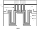
- etching etching
- etching etching usually stops on the electrode layer, and an etch selectivity of the electrode layer and the dielectric layer is usually low. Therefore, when the contact hole CT is manufactured, etching is prone to cause damage to an electrode, that is, a process difficulty of etching is high.
- This application provides a capacitor component and a manufacturing method thereof, and an electronic device, and provides a DTC of a new structure, to reduce a manufacturing process difficulty of the component.
- the capacitor component includes a first structure layer, a metal routing layer, a first connection pad, and a second connection pad.
- a trench and a plurality of metal vias are disposed in the first structure layer, and an opening is provided at a bottom of the trench.
- the metal routing layer is located at the bottom of the trench and is exposed in the opening.
- a plurality of electrode layers and a plurality of first dielectric layers are alternately filled in the trench. Each of the first connection pad and the second connection pad is connected to the metal routing layer through the metal via.
- the plurality of electrode layers include a first electrode layer, a second electrode layer, and at least one intermediate electrode layer located between the first electrode layer and the second electrode layer.
- the first electrode layer covers an inner side wall of the trench, and is in contact with the metal routing layer at the opening.
- the first connection pad or the second connection pad covers a surface of the second electrode layer.
- the intermediate electrode layer extends from the trench, and is connected to the metal routing layer through the metal via. Two adjacent electrode layers are electrically connected to the first connection pad and the second connection pad respectively.
- the metal routing layer is disposed at the bottom of the trench, and the plurality of metal vias are disposed on a side surface of the trench.
- an electrode layer (the second electrode layer) at a top layer may be directly connected to a connection pad above, and another electrode layer is led out from a bottom to the connection pad through the metal routing layer and the metal via.
- an electrode layer (the first electrode layer) at a bottom layer is directly connected to the metal routing layer at the bottom of the trench, and is led upward to the connection pad through the metal via; and the intermediate electrode layer is connected to the metal routing layer through the metal via, and is led upward to the connection pad through the metal via.
- the electrode layer is led out to the connection pad by combining the metal routing layer and the metal via, and no contact hole is required. This can reduce a manufacturing process difficulty and manufacturing costs, and avoid problems such as an electrode layer loss caused by manufacturing the contact hole.
- the metal routing layer includes a first trace and a second trace.
- the first trace is located at the bottom of the trench and is exposed in the opening.
- the first trace and the second trace are respectively connected to the first connection pad and the second connection pad through different metal vias.
- the first trace and the second trace are located at a same layer.
- the first structure layer includes an upper structure layer and a lower structure layer, and the upper structure layer is located on a side that is of the lower structure layer and that is away from the first trace.
- the first trace is located at the bottom of the trench and is exposed in the opening, and the first trace is connected to the first connection pad through a metal via located in the upper structure layer and a metal via located in the lower structure layer.
- the second trace is located between the upper structure layer and the lower structure layer, and the second trace is connected to the second connection pad through a metal via located in the upper structure layer.
- the plurality of electrode layers include one intermediate electrode layer.
- the intermediate electrode layer is connected to the second trace through the metal via.
- the first connection pad covers the second electrode layer.
- the plurality of electrode layers include two intermediate electrode layers.
- the two intermediate electrode layers are a third electrode layer and a fourth electrode layer, and the third electrode layer is closer to the first electrode layer than the fourth electrode layer.
- the third electrode layer is connected to the second trace through the metal via, and the fourth electrode layer is connected to the first trace through the metal via.
- the second connection pad covers the second electrode layer.
- the first dielectric layer includes at least one of HfO 2 , ZrO 2 , and Al 2 O 3 , to increase capacitance density of the capacitor component.
- any two adjacent film layers in the plurality of electrode layers and the plurality of first dielectric layers are a first layer and a second layer respectively, and the first layer is closer to the metal routing layer than the second layer.
- the first layer and the second layer extend from the trench, and an edge of the second layer exceeds an edge of the first layer.
- the metal via is a copper via, so that a pitch (pitch) between metal vias and a pitch between the metal via and the trench can be reduced, thereby improving the capacitance density of the capacitor component.
- the first structure layer includes at least one of a dielectric layer and a semiconductor layer.
- An embodiment of this application further provides a manufacturing method of a capacitor component.
- the manufacturing method includes: providing a substrate, where the substrate includes a first surface and a second surface that are disposed opposite to each other; manufacturing, on the first surface of the substrate, a metal routing layer including a first trace and a second trace; manufacturing a trench and a plurality of metal vias along the second surface of the substrate, and exposing the first trace at a bottom of the trench; alternately filling a plurality of electrode layers and a plurality of first dielectric layers in the trench in sequence, where the plurality of electrode layers include a first electrode layer, a second electrode layer, and at least one intermediate electrode layer located between the first electrode layer and the second electrode layer, the first electrode layer covers an inner side wall of the trench, and is in contact with the first trace at an opening, and the intermediate electrode layer extends from the trench, and is connected to the first trace or the second trace through the metal via; and forming a first connection pad and a second connection pad, where the first connection pad or the second connection
- An embodiment of this application further provides a manufacturing method of a capacitor component.
- the manufacturing method includes: manufacturing, on a substrate, a metal routing layer including a first trace and a second trace.
- a second dielectric layer is manufactured on the metal routing layer, a trench and a plurality of metal vias are manufactured along an upper surface of the second dielectric layer, and the first trace is exposed at a bottom of the trench.
- a plurality of electrode layers and a plurality of first dielectric layers are alternately filled in the trench in sequence, where the plurality of electrode layers include a first electrode layer, a second electrode layer, and at least one intermediate electrode layer located between the first electrode layer and the second electrode layer; the first electrode layer covers an inner side wall of the trench, and is in contact with the first trace at an opening; and the intermediate electrode layer extends from the trench, and is connected to the first trace or the second trace through the metal via.
- a first connection pad and a second connection pad are formed, where the first connection pad or the second connection pad covers a surface of the second electrode layer, and the first connection pad and the second connection pad are respectively connected to the first trace and the second trace through metal vias; and two adjacent electrode layers are electrically connected to the first connection pad and the second connection pad respectively.
- An embodiment of this application further provides an electronic device.
- the electronic device includes a circuit board and the capacitor component provided in any one of the foregoing possible implementations.
- the capacitor component is electrically connected to the circuit board.
- connection may be an electrical connection, or a mechanical connection; the connection may be a fastened connection, a detachable connection, or an integrated connection; and the connection may be a direct connection, or may be an indirect connection through an intermediate medium, or may be a connection inside two elements.
- connection may be an electrical connection, or a mechanical connection; the connection may be a fastened connection, a detachable connection, or an integrated connection; and the connection may be a direct connection, or may be an indirect connection through an intermediate medium, or may be a connection inside two elements.
- the terms “include”, “have”, and any variant thereof are intended to cover non-exclusive inclusion.
- a process, method, system, product, or device that includes a series of steps or units is not necessarily limited to those steps or units expressly listed, but may include other steps or units not expressly listed or inherent to such a process, method, product, or device.
- An embodiment of this application provides an electronic device.
- the electronic device includes a printed circuit board (printed circuit board, PCB, also referred to as a printed circuit board) and a capacitor component electrically connected to the circuit board.
- the capacitor component uses a deep trench capacitor (DTC) of a new structure, and uses a Damascus process.
- DTC deep trench capacitor
- a plurality of electrode layers are led out from a bottom in a manner of combining a metal routing layer and a metal via, thereby avoiding a problem in the conventional technology that the electrode layer is led out from a top through a contact hole, which results in a high manufacturing process difficulty.
- a disposition form of the electronic device is not limited in this application.
- the electronic device may be an electronic product like a mobile phone, a tablet computer, a notebook computer, an in-vehicle computer, a smartwatch, a smart band, or a server.
- the capacitor component may be any component disposed with a deep trench capacitor (DTC), for example, an interposer (interposer) in a 2.5D package structure, an artificial intelligence chip, a high-performance computing chip, or a server logic chip.
- DTC deep trench capacitor
- the capacitor component includes a first structure layer 100, a metal routing layer 200 below the first structure layer 100, and connection pads (P1 and P2) above the first structure layer 100.
- the metal routing layer 200 may include a first trace L1 and a second trace L2. According to an actual requirement, each of the first trace L1 and the second trace L2 may be connected to another component below through a metal via. This is not limited in this application.
- At least one trench 101 and a plurality of metal vias are disposed in the first structure layer 100.
- a plurality of electrode layers (E1, E2, E3, and E4) and a plurality of first dielectric layers 10 are alternately filled inside the trench 101.
- the plurality of electrode layers (E1, E2, E3, and E4) and the plurality of first dielectric layers 10 may extend from the trench 101.
- connection pads located above the first structure layer 100 may include a first connection pad P1 and a second connection pad P2.
- the first connection pad P1 is electrically connected to the first trace L1 through a first metal via V1
- the second connection pad P2 is electrically connected to the second trace L2 through a second metal via V2.
- the first connection pad P1 may be electrically connected to the first trace L1 through one or more first metal vias V1.
- FIG. 2 and FIG. 3 show only one first metal via V1.
- Disposition of the second metal via V2, and disposition of a third metal via and a fourth metal via in the following are similar.
- the plurality of electrode layers may be at least three electrode layers.
- three electrode layers (E1, E2, and E3) and two first dielectric layers 10 may be disposed in the trench 101.
- the three electrode layers from bottom to top are sequentially: the first electrode layer E1, the third electrode layer E3, and the second electrode layer E2.
- One first dielectric layer 10 is disposed between the first electrode layer E1 and the third electrode layer E3, and one first dielectric layer 10 is disposed between the third electrode layer E3 and the second electrode layer E2.
- four electrode layers (E1, E2, E3, and E4) and three first dielectric layers 10 may be disposed in the trench 101.
- the four electrode layers from bottom to top are sequentially: the first electrode layer E1, the third electrode layer E3, the fourth electrode layer E4, and the second electrode layer E2.
- One first dielectric layer 10 is disposed between the first electrode layer E1 and the third electrode layer E3, one first dielectric layer 10 is disposed between the third electrode layer E3 and the fourth electrode layer E4, and one first dielectric layer 10 is disposed between the fourth electrode layer E4 and the second electrode layer E2.
- any two adjacent electrode layers are electrically connected to two different connection pads (P1 and P2).
- connection pads P1 and P2
- electrode layers located at an odd-numbered layer are connected to a same connection pad
- electrode layers located at an even-numbered layer are connected to the other connection pad, so that a voltage difference can be formed between any two adjacent electrode layers.
- a specific connection manner of the plurality of electrode layers in the trench 101 may be as follows.
- the first electrode layer E1 located at the bottommost covers an inner side wall of the trench 101, and is in contact with the first trace L1 at the opening at the bottom of the trench 101.
- the second electrode layer E2 located at the topmost is directly covered by the first connection pad P1 or the second connection pad P2 based on a number of a layer at which the second electrode layer E2 is located.
- the second electrode layer E2 is located at a 3 rd layer, and the first connection pad P1 directly covers the second electrode layer E2, to implement an electrical connection between the second electrode layer E2 and the first connection pad P1.
- the second electrode layer E2 is located at a 4 th layer, and the second connection pad P2 directly covers the second electrode layer E2, to implement an electrical connection between the second electrode layer E2 and the second connection pad P2.
- An intermediate electrode layer located between the first electrode layer E1 and the second electrode layer E2 may be connected to the first trace L1 or the second trace L2 through a metal via based on a number of a layer at which the intermediate electrode layer is located.
- one intermediate electrode layer (namely, the third electrode layer E3) is disposed between the first electrode layer E1 and the second electrode layer E2.
- the third electrode E3 is directly connected to the second trace L2 through the third metal via V3, and is electrically connected to the second connection pad P2 through the second trace L2 and the second metal via V2.
- two intermediate electrode layers are disposed between the first electrode layer E1 and the second electrode layer E2, namely, the third electrode layer E3 and the fourth electrode layer E4.
- the third electrode layer E3 is located between the first electrode layer E1 and the fourth electrode layer E4, and the fourth electrode layer E4 is located between the third electrode layer E3 and the second electrode layer E2.
- the third electrode layer E3 is directly connected to the second trace L2 through the third metal via V3, and is electrically connected to the second connection pad P2 through the second trace L2 and the second metal via V2.
- the fourth electrode layer E4 is directly connected to the first trace L1 through the fourth metal via V4, and is electrically connected to the first connection pad P1 through the first trace L1 and the first metal via V1.
- five or more electrode layers may be alternatively disposed in the groove 101, and an intermediate electrode layer located between the first electrode layer E1 and the second electrode layer E2 may be disposed with reference to a connection manner of the intermediate electrode layer in FIG. 2 and FIG. 3 . Details are not described herein again.
- the metal routing layer 200 is disposed at the bottom of the trench 101, and a plurality of metal vias (V1, V2, V3, and V4) are disposed on a side surface of the trench 101.
- the electrode layer (the second electrode layer E2) at a top layer may be directly connected to the connection pad above, and another electrode layer (E1, E3, or E4) is led out from the bottom to the connection pad (P1 or P2) through the metal routing layer 200 and the metal via.
- the electrode layer (the first electrode layer E1) at a bottom layer is directly connected to the metal routing layer 200 at the bottom of the trench 101, and is led upward to the connection pad through the metal via; and the intermediate electrode layer (E3 or E4) is connected to the metal routing layer 200 through the metal via, and then is led upward to the connection pad through the metal via.
- the electrode layer is led out to the connection pad (P1 or P2) by combining the metal routing layer 200 and the metal via, and no contact hole is required. This can reduce a manufacturing process difficulty and manufacturing costs, and avoid problems such as an electrode layer loss caused by manufacturing the contact hole.
- a specific material of the first dielectric layer 10 disposed between two adjacent electrode layers is not limited in this application, and may be selected according to an actual requirement.
- the first dielectric layer 10 may use a high dielectric constant material (namely, an HK material), for example, one or more of HfO 2 , ZrO 2 , and Al 2 O 3 .
- a high dielectric constant material namely, an HK material
- the first dielectric layer 10 may use a ZrO 2 /Al 2 O 3 /ZrO 2 multi-film structure (namely, ZAZ).
- ZAZ ZrO 2 /Al 2 O 3 /ZrO 2 multi-film structure
- the plurality of electrode layers (E1, E2, E3, and E4) and the plurality of first dielectric layers 10 in the trench 101 may be disposed to extend from the trench 101, and in any two adjacent film layers, an edge of an upper film layer (which may alternatively be referred to as a second layer) exceeds an edge of a lower film layer (which may alternatively be referred to as a first layer).
- an edge of the first dielectric layer 10 on an upper surface of the first electrode layer E1 exceeds an edge of the first electrode layer E1
- an edge of the second electrode layer E1 exceeds an edge of the first dielectric layer 10 located on a lower surface of the second electrode layer E1.
- an etching process stops on a surface of the first structure layer 100, thereby reducing a difficulty of the etching process.
- an etching stop layer SL may be disposed between the first structure layer 100 and the metal routing layer 200.
- the etching stop layer SL has a significantly lower etching rate, so that it can be ensured that when the trench 101 and the metal via (V1, V2, V3, or V4) are manufactured in the first structure layer 100, etching can stop in the etching stop layer SL evenly, thereby improving uniformity and consistency of the etching process.
- a disposition form, a material, and the like of the first structure layer 100 may be specifically disposed based on an application scenario of the capacitor component. This is not limited in this application.
- the first structure layer 100 may be a single-layer structure.
- the first structure layer 100 may alternatively be a multi-layer structure.
- the first structure layer 100 may be a substrate in the capacitor component, for example, a Si substrate.
- the first structure layer 100 may be a dielectric layer, for example, a SiO 2 layer. However, this is not limited thereto.
- connection pads (P1 and P1) are located on a back side (namely, an active side) of the substrate, and another part may be manufactured on a front side of the substrate according to an actual requirement.
- a substrate 400 in the capacitor component may be located below the metal routing layer 200.
- the first structure layer 100 may include a substrate and a dielectric layer. In some embodiments, the first structure layer 100 may include a plurality of dielectric layers. This is not limited in this application, and may be set according to an actual requirement.
- the first trace L1, the second trace L2, and a related metal via may be adjusted according to an actual requirement.
- the first structure layer 100 may include a lower structure layer 11 and an upper structure layer 12.
- an etching stop layer SL may be disposed between the lower structure layer 11 and the upper structure layer 12, to improve uniformity and consistency of an etching process.
- the first trace L1 and the second trace L2 may be distributed in different metal routing layers, and a metal routing layer in which the first trace L1 is located below the lower structure layer 11, and is exposed in the opening at the bottom of the trench 101.
- the metal via connected between the first trace L1 and the first connection pad P1 and the metal via between the first trace L1 and the fourth electrode layer E4 may be disposed in a segment manner, so that a manufacturing difficulty can be reduced. As shown in FIG.
- the metal via connected between the first trace L1 and the first connection pad P1 may include two metal vias (V1_a and V1_b) manufactured in the upper structure layer 12 and the lower structure layer 11 in segment
- the metal via between the first trace L1 and the fourth electrode layer E4 may include two metal vias (V4_a and V4_b) manufactured in the upper structure layer 12 and the lower structure layer 11 in segment.
- each trench capacitor unit may be disposed in the capacitor component.
- the trench 101, the connection pads (P1 and P2), and the like may be disposed according to an actual requirement.
- a quantity, a shape, a depth, and the like of the trench 101 disposed in a single trench capacitor unit (DTC unit) are not limited in this application, and may be set according to an actual requirement.
- a trench 101 used in a single trench capacitor unit may be one or a combination of a rectangular trench, a circular trench, a cross trench, a wave trench, and another type of trench.
- a trench structure with a large inner surface area may be selected according to a requirement.
- quantities, shapes, sizes, and the like of the first connection pad P1 and the second connection pad P2 in a single trench capacitor unit are not limited in this application, and may be set according to an actual requirement.
- one first connection pad P1 and one second connection pad P2 may be disposed in a single trench capacitor unit (DTC unit).
- DTC unit trench capacitor unit
- a plurality of metal vias connected to the first trace L1 are all connected to the first connection pad P1
- a plurality of metal vias connected to the second trace L2 are all connected to the second connection pad P2.
- a plurality of first connection pads P1 and a plurality of second connection pads P2 may be disposed in a single trench capacitor unit (DTC unit), and different connection pads are connected to different metal vias.
- DTC unit trench capacitor unit
- the aluminum via is filled through physical vapor deposition (physical vapor deposition, PVD), and a depth-width ratio of the aluminum via is generally not greater than 2: 1.
- the copper via may be filled through an electro-chemical plating (electro-chemical plating, ECP) process, so that filling with a high depth-width ratio may be implemented, and a depth-width ratio of the copper via may be more than 5:1. That is, when hole depths are the same, the copper via can be filled with a smaller diameter, thereby obtaining a smaller pitch (pitch).
- all of the metal vias (V1, V2, V3, and V4) disposed in the first structure layer 100 may be copper vias, so that a pitch (pitch) between the metal vias can be reduced, and the capacitance density of the capacitor component can be improved.
- a manufacturing method of a capacitor component is provided by using an example in which a substrate is used as a first structure layer 100. As shown in FIG. 8 , the manufacturing method may include the following steps.
- Step 11 With reference to (a) in FIG. 9 , provide a substrate 100_a, where the substrate 100_a includes a first surface A1 and a second surface A2 that are disposed opposite to each other.
- the substrate 100_a may be a silicon substrate.
- another film layer or part may be disposed on the first surface A1 and the second surface A2 of the silicon substrate. This is not limited in this application.
- Step 12 With reference to (b) in FIG. 9 , manufacture, on the first surface A1 of the substrate 100_a, a metal routing layer 200 including a first trace L1 and a second trace L2.
- a metal layer may be formed on the first surface A1 of the silicon substrate (100_a) through a metal deposition process in step 12, and the metal layer is etched through an etching process, to form the first trace L1 and the second trace L2, that is, to form the metal routing layer 200.
- an etching stop layer SL may be first manufactured on the first surface A1 of the substrate 100_a.
- the etching stop layer SL refer to the foregoing descriptions. Details are not described herein again.
- Step 13 With reference to (a) and (b) in FIG. 10 , manufacture a plurality of metal vias (V1, V2, and V3) and a trench 101 along the second surface A2 of the substrate 100_a, and expose the first trace L1 at a bottom of the trench 101.
- the plurality of metal vias (V1, V2, and V3) are manufactured along the second surface A2 of the substrate 100_a through atomic layer deposition (atomic layer deposition, ALD) and an etching process, where bottoms of some metal vias (V1) are connected to the first trace L1, and bottoms of some metal vias (V2 and V3) are connected to the second trace L2.
- atomic layer deposition atomic layer deposition, ALD
- a plurality of trenches 101 are manufactured through an etching process along a position that is on the second surface A2 of the substrate 100_a and that corresponds to the first trace L1, and the first trace L1 is exposed at the bottom of the trench 101.
- Step 14 With reference to (a) in FIG. 11 , alternately fill a plurality of electrode layers (E1, E2, and E2) and a plurality of first dielectric layers 10 in the trench 101.
- a first electrode layer E1, a first dielectric layer 10, a third electrode layer E3, a first dielectric layer 10, and a second electrode layer E2 may be sequentially manufactured in step 14, that is, three electrode layers and two first dielectric layers 10 are formed.
- the first electrode layer E1 covers an inner side wall of the trench 101, and is in contact with the first trace L1 at the opening; and the third electrode layer E3 extends from the trench 101, and may be connected to the first trace L1 through the metal via V3.
- the second electrode layer E2 is located at a top layer.
- each film layer of the plurality of electrode layers (E1, E2, and E2) and the plurality of first dielectric layers 10 may be separately manufactured through a deposition process and an etching process, and it is ensured that an edge of an upper film layer in two adjacent film layers exceeds an edge of a lower film layer, so that the etching process can stop on a surface of the substrate 100_a, thereby reducing a manufacturing process difficulty.
- a SiO 2 layer may be deposited in the groove 101 as a passivation layer.
- Step 15 With reference to (b) in FIG. 11 , form a first connection pad P1 and a second connection pad P2.
- the first connection pad P1 is directly manufactured on a surface of the second electrode layer E2, and is electrically connected to the second electrode layer E2.
- the first connection pad P1 is connected to the first trace L1 through the metal via V1
- the second connection pad P2 is connected to the second trace L2 through the metal via V2, so that two adjacent electrode layers are electrically connected to different connection pads.
- the first connection pad P1 and the second connection pad P2 may be manufactured through an aluminum deposition process and an etching process.
- step 15 other subsequent processes may be performed according to a requirement on the capacitor component.
- a passivation layer may be manufactured, and a window is opened through etching at positions corresponding to the first connection pad P1 and the second connection pad P2 on the passivation layer, to ensure electrical connections between the first connection pad P1 and the second connection pad P2 and another external component.
- the foregoing related steps may be correspondingly adjusted according to an actual requirement on the capacitor component.
- a specific manufacturing process may be adjusted by using step 13 and step 14.
- a case in which four electrode layers are filled in the groove 101 is used as an example.
- the plurality of metal vias may be manufactured along the second surface A2 of the substrate 100_a in step 13, where bottoms of the metal vias (V1 and V4) are connected to the first trace L1, and bottoms of the metal vias (V2 and V3) are connected to the second trace L2.
- the first electrode layer E1, the first dielectric layer 10, the third electrode layer E3, the first dielectric layer 10, the third electrode layer E3, the first dielectric layer 10, and the second electrode layer E2 may be sequentially manufactured in the trench 101 in step 14, that is, four electrode layers and three first dielectric layers 10 are formed.
- the first electrode layer E1 covers an inner side wall of the trench 101, and is in contact with the first trace L1 at the opening; and the third electrode layer E3 extends from the trench 101, and may be connected to the first trace L1 through the metal via V3.
- the fourth electrode layer E4 extends from the trench 101, and may be connected to the second trace L2 through the metal via V4.
- the second electrode layer E2 is located at a top layer.
- a manufacturing method of a capacitor component is provided by using an example in which a dielectric layer (a second dielectric layer) is used as a first structure layer 100. As shown in FIG. 13 , the manufacturing method may include the following steps.
- Step 21 With reference to FIG. 5 , manufacture, on a substrate 400, a metal routing layer 200 including a first trace L1 and a second trace L2.
- the substrate 400 may be a silicon substrate. According to an actual requirement on the component, before the metal routing layer 200 is manufactured on a surface of the silicon substrate, another film layer, for example, a dielectric layer 300, may be manufactured.
- step 21 refer to related descriptions of step 12. Details are not described herein again.
- Step 22 With reference to FIG. 5 , manufacture a second dielectric layer (100) on the metal routing layer 200, manufacture a plurality of metal vias (V1, V2, and V3) and a trench 101 along an upper surface of the second dielectric layer (100), and expose the first trace L1 at a bottom of the trench 101.
- step 22 refers to related descriptions of step 13. Details are not described herein again.
- an etching stop layer SL may be first manufactured on a surface of the metal routing layer 200.
- Step 23 With reference to FIG. 5 , alternately fill a plurality of electrode layers (E1, E2, and E2) and a plurality of first dielectric layers 10 in the trench 101.
- step 23 refers to related descriptions of step 14. Details are not described herein again.
- Step 24 With reference to FIG. 5 , form a first connection pad P1 and a second connection pad P2.
- step 24 refer to related descriptions of step 15. Details are not described herein again.
- sequence numbers of the foregoing manufacturing processes do not mean execution sequences.
- the execution sequences of the manufacturing processes should be determined based on specific functions and internal logic of the components, and should not be construed as any limitation on the implementation processes of embodiments of this application.
Landscapes
- Engineering & Computer Science (AREA)
- Power Engineering (AREA)
- Microelectronics & Electronic Packaging (AREA)
- Manufacturing & Machinery (AREA)
- Semiconductor Integrated Circuits (AREA)
- Internal Circuitry In Semiconductor Integrated Circuit Devices (AREA)
Applications Claiming Priority (1)
| Application Number | Priority Date | Filing Date | Title |
|---|---|---|---|
| CN202310427258.9A CN118800757A (zh) | 2023-04-12 | 2023-04-12 | 电容器件及其制作方法、电子设备 |
Publications (1)
| Publication Number | Publication Date |
|---|---|
| EP4447079A1 true EP4447079A1 (de) | 2024-10-16 |
Family
ID=90365403
Family Applications (1)
| Application Number | Title | Priority Date | Filing Date |
|---|---|---|---|
| EP24163564.8A Pending EP4447079A1 (de) | 2023-04-12 | 2024-03-14 | Kondensatorkomponente und herstellungsverfahren dafür sowie elektronische vorrichtung |
Country Status (2)
| Country | Link |
|---|---|
| EP (1) | EP4447079A1 (de) |
| CN (1) | CN118800757A (de) |
Citations (3)
| Publication number | Priority date | Publication date | Assignee | Title |
|---|---|---|---|---|
| US6972451B2 (en) * | 2002-05-15 | 2005-12-06 | Stmicroelectronics S.A. | Trench capacitor in a substrate with two floating electrodes independent from the substrate |
| US20210020737A1 (en) * | 2019-04-24 | 2021-01-21 | Shenzhen GOODIX Technology Co., Ltd. | Capacitor and method for producing the same |
| EP3786991A1 (de) * | 2019-05-29 | 2021-03-03 | Shenzhen Goodix Technology Co., Ltd. | Kondensator und herstellungsverfahren dafür |
-
2023
- 2023-04-12 CN CN202310427258.9A patent/CN118800757A/zh active Pending
-
2024
- 2024-03-14 EP EP24163564.8A patent/EP4447079A1/de active Pending
Patent Citations (3)
| Publication number | Priority date | Publication date | Assignee | Title |
|---|---|---|---|---|
| US6972451B2 (en) * | 2002-05-15 | 2005-12-06 | Stmicroelectronics S.A. | Trench capacitor in a substrate with two floating electrodes independent from the substrate |
| US20210020737A1 (en) * | 2019-04-24 | 2021-01-21 | Shenzhen GOODIX Technology Co., Ltd. | Capacitor and method for producing the same |
| EP3786991A1 (de) * | 2019-05-29 | 2021-03-03 | Shenzhen Goodix Technology Co., Ltd. | Kondensator und herstellungsverfahren dafür |
Also Published As
| Publication number | Publication date |
|---|---|
| CN118800757A (zh) | 2024-10-18 |
Similar Documents
| Publication | Publication Date | Title |
|---|---|---|
| US11222869B2 (en) | Dummy TSV to improve process uniformity and heat dissipation | |
| US8618651B1 (en) | Buried TSVs used for decaps | |
| US20200137889A1 (en) | Capacitor having through hole structure and manufacturing method therefor | |
| EP3734656B1 (de) | In-situ-gehäuseintegrierte dünnschichtkondensatoren zur leistungsabgabe | |
| EP3985724A1 (de) | Halbleitervorrichtung und verfahren zur herstellung davon | |
| US9257322B2 (en) | Method for manufacturing through substrate via (TSV), structure and control method of TSV capacitance | |
| EP4447079A1 (de) | Kondensatorkomponente und herstellungsverfahren dafür sowie elektronische vorrichtung | |
| CN118039605A (zh) | 半导体封装结构及其制备方法 | |
| CN113272941A (zh) | 半导体模块及其制造方法 | |
| WO2023035433A1 (zh) | 半导体结构的形成方法及半导体结构 | |
| CN119451561A (zh) | Mim电容器及其制造方法 | |
| TWI746483B (zh) | 使用雙微影製程之高效能整合射頻被動元件 | |
| CN114597166B (zh) | 一种存储器及其制备方法和存储系统 | |
| CN210272338U (zh) | 焊盘结构及半导体器件 | |
| EP4593079A1 (de) | Halbleiterstruktur und herstellungsverfahren dafür | |
| CN119451562A (zh) | 金属-绝缘体-金属电容器及其制造方法 | |
| CN119542328B (zh) | 半导体结构及其制作方法和半导体器件 | |
| EP4489071A1 (de) | Halbleiterbauelement mit halbleitergehäuse mit in einer dielektrischen schicht eingebettetem kondensator | |
| CN119542329B (zh) | 半导体结构及其制作方法和半导体器件 | |
| US20250218879A1 (en) | Resist tenting and plating in core cavity for component attachment | |
| US20190108943A1 (en) | High voltage capacitors and methods of manufacturing the same | |
| EP4576203A1 (de) | Chipgehäusestruktur, herstellungsverfahren dafür und elektronische vorrichtung | |
| EP4709074A1 (de) | Halbleiterbauelement und herstellungsverfahren dafür sowie dreidimensionaler dynamischer direktzugriffsspeicher | |
| CN216671616U (zh) | 晶片封装的导接线路结构 | |
| EP3958293B1 (de) | Verfahren zur herstellung eines lochs in einer halbleiterbauelement |
Legal Events
| Date | Code | Title | Description |
|---|---|---|---|
| PUAI | Public reference made under article 153(3) epc to a published international application that has entered the european phase |
Free format text: ORIGINAL CODE: 0009012 |
|
| STAA | Information on the status of an ep patent application or granted ep patent |
Free format text: STATUS: THE APPLICATION HAS BEEN PUBLISHED |
|
| AK | Designated contracting states |
Kind code of ref document: A1 Designated state(s): AL AT BE BG CH CY CZ DE DK EE ES FI FR GB GR HR HU IE IS IT LI LT LU LV MC ME MK MT NL NO PL PT RO RS SE SI SK SM TR |
|
| STAA | Information on the status of an ep patent application or granted ep patent |
Free format text: STATUS: REQUEST FOR EXAMINATION WAS MADE |
|
| 17P | Request for examination filed |
Effective date: 20250416 |