EP4450978A1 - Système de capteur de courant - Google Patents
Système de capteur de courant Download PDFInfo
- Publication number
- EP4450978A1 EP4450978A1 EP24166728.6A EP24166728A EP4450978A1 EP 4450978 A1 EP4450978 A1 EP 4450978A1 EP 24166728 A EP24166728 A EP 24166728A EP 4450978 A1 EP4450978 A1 EP 4450978A1
- Authority
- EP
- European Patent Office
- Prior art keywords
- conductor
- current sensor
- longitudinal axis
- central longitudinal
- hole
- Prior art date
- Legal status (The legal status is an assumption and is not a legal conclusion. Google has not performed a legal analysis and makes no representation as to the accuracy of the status listed.)
- Pending
Links
Images


Classifications
-
- G—PHYSICS
- G01—MEASURING; TESTING
- G01R—MEASURING ELECTRIC VARIABLES; MEASURING MAGNETIC VARIABLES
- G01R15/00—Details of measuring arrangements of the types provided for in groups G01R17/00 - G01R29/00, G01R33/00 - G01R33/26 or G01R35/00
- G01R15/14—Adaptations providing voltage or current isolation, e.g. for high-voltage or high-current networks
- G01R15/20—Adaptations providing voltage or current isolation, e.g. for high-voltage or high-current networks using galvano-magnetic devices, e.g. Hall-effect devices, i.e. measuring a magnetic field via the interaction between a current and a magnetic field, e.g. magneto resistive or Hall effect devices
- G01R15/207—Constructional details independent of the type of device used
Definitions
- sensors are used to perform various functions in a variety of applications.
- Some sensors include one or magnetic field sensing elements, such as a Hall effect element or a magnetoresistive element, to sense a magnetic field associated with proximity or motion of a target object, such as a ferromagnetic object in the form of a gear or ring magnet, or to sense a current, as examples.
- Sensor integrated circuits are widely used in automobile control systems and other safety-critical applications. There are a variety of specifications that set forth requirements related to permissible sensor quality levels, failure rates, and overall functional safety.
- a system comprising: a printed circuit board; a first conductor having a first central longitudinal axis, the first conductor having a first through-hole that is formed therein; a second conductor having a second central longitudinal axis; and a first current sensor that is mounted on the printed circuit board, the first current sensor being disposed at least partially inside the first through-hole, the first current sensor including a first pair of magnetic field sensing elements, the magnetic field sensing elements in the first pair being aligned with a first alignment axis that is arranged at a first angle relative to the second central longitudinal axis, the first angle being less than 75 degrees.
- a system comprising: a printed circuit board; a first conductor having a first central longitudinal axis, the first conductor having a first through-hole that is formed therein; a second conductor having a second central longitudinal axis; and a first current sensor that is mounted on the printed circuit board, the first current sensor being disposed at least partially inside the first through-hole, the first current sensor including a first pair of magnetic field sensing elements, the magnetic field sensing elements in the first pair being aligned with a first alignment axis that is substantially parallel to the second central longitudinal axis.
- a system comprising: a printed circuit board; a first conductor having a first central longitudinal axis, the first conductor having a first notch and a second notch; a second conductor having a second central longitudinal axis; and a first current sensor that is mounted on the printed circuit board, the first current sensor being disposed at least partially inside the first notch, the first current sensor including a first pair of magnetic field sensing elements, the magnetic field sensing elements in the first pair being aligned with a first alignment axis.
- a system comprising: a first conductor having a first central longitudinal axis, the first conductor having a first through-hole that is formed therein; a second conductor that is disposed adjacent to the first conductor, the first conductor having a second central longitudinal axis, the second conductor having a second through-hole that is formed therein; a printed circuit board that is inserted through the first through-hole and the second through-hole, the printed circuit board having a first current sensor and a second current sensor mounted thereon, wherein, the first current sensor is disposed inside the first through-hole and includes a first pair of magnetic field sensing elements, the magnetic field sensing elements in the first pair having respective axes of maximum sensitivity that are substantially perpendicular to the first central longitudinal axis, and wherein, the second current sensor is disposed inside the second through-hole and includes a second pair of magnetic field sensing elements, the magnetic field sensing elements in the second pair having respective axes of maximum sensitivity that are substantially perpendicular to the first central longitudinal axi
- a system comprising: a printed circuit board; a conductor having a pair of notches formed therein that define a mid-portion of the conductor, the mid portion being disposed between a first end portion and a second end portion of the conductor, the mid portion extending along an axis Q-Q that is arrented at a first angle relative to a central longitudinal axis A3-A3, the first angle being less than 75 degrees; a current sensor that is mounted on the printed circuit board, the current sensor being disposed at least partially inside the through-hole, the current sensor including a pair of magnetic field sensing elements that are aligned with an axis G-G, the axis G-G being arranged at a second angle relative to the central longitudinal axis A3-A3, the second angle being less than 75 degrees.
- FIG. 1 is a diagram of an example of a system 100, according to aspects of the disclosure.
- the system 100 may include a controller 101 and a power source 102 that is coupled to an electric motor 104 via an interface 106.
- the interface 106 may include a printed circuit board (PCB) 107.
- the PCB 107 may include conductors 108A-C and conductive traces 112A-C.
- Each of the conductive traces 112A-C may include one or more metal layers (or layers of another conductive material) that are at least partially encapsulated in a dielectric material of the PCB 107.
- Each of the conductors 108A-C may also include one or more metal layers (or layers of another conductive material) that are at least partially encapsulated in the dielectric material of the PCB 107.
- the conductive traces 112A-C may differ in one or more characteristics from the conductors 108A-C. According to the example of FIG.
- each of the conductors 108A-C may be configured to carry higher currents than any of the conductive traces 112-C. Additionally or alternatively, in some implementations, each of the conductors 108A-C may have a larger cross-section than any of the conductive traces 112-C. Additionally or alternatively, in some implementations, each of the conductors 108A-C may have larger width and/or thickness than any of the conductive traces 112-C.
- Each of the conductors 108A-C may be used to deliver, to the electric motor 104, current that is supplied by the power source 102.
- the controller 101 may be coupled to the current sensors 110A-C via the conductive traces 112A-C.
- the controller 101 may use the current sensors 110A-C to measure the level of the current that is being supplied by the power source 102 to the electric motor 104 and make adjustments to the operation of the power source 102 and/or the electric motor 104 in response to the measurements.
- the controller 101 may use current sensor 110A to measure the current carried by conductor 108A, current sensor 110B to measure current carried by conductor 108B, and current sensor 110C to measure current carried by conductor 108C.
- the interface 106 consists of three conductors 108, alternative implementations are possible in which the interface 106 consists of any number of conductors 108 ( e.g., only one conductor, only two conductors, five conductors, etc .). Although in the example of FIG. 1 the interface 106 is used to electrically couple a motor to a power source, it will be understood that the present disclosure is not limited to any specific application of the interface 106.
- any of conductors 108A-C may have a width between 8mm and 30mm, whereas each of the conductive traces 112A-C may have a width between 0.1mm and 1mm.
- each of the conductors 108A-C may include one or more layers (e.g. ,1-10 layers, etc.), each having thickness between 20 ⁇ m to 200 ⁇ m.
- conductors 108A-C may be adapted to carry much higher currents than the conductive traces 112A-C.
- each of conductors 108A-C may be configured to carry current in the range of 50-500A, whereas each of the conductive traces may be configured to carry current in the range of 0.01A-5A.
- both the conductors 108A-C and the conductive traces 112A-C may be embedded in the PCB 107.
- both the conductors 110A-C and the conductive traces 112A-C may be formed by using standard lithographic techniques that are normally applied in PCB manufacturing.
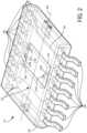
- FIG. 2 is a diagram of an example of a current sensor 110, according to aspects of the disclosure. As the numbering suggests, the current sensor 110 may be the same or similar to any of the current sensors 110A-C, which are shown in FIG. 1 . It will be understood that FIG. 2 is provided as an example only, and the interface 106 is not limited to using any specific type of current sensor.
- current sensor 110 include a lead frame 202 and a die 208 supporting magnetic field sensing elements 210A and 210B.
- Lead frame 202 includes a die attach paddle 204 and a plurality of leads 206.
- Die 208 is attached to die attach paddle 204, as may be achieved with an adhesive layer 207. While a single semiconductor die 208 is shown, the current sensor 110 can include more than one die, with each such die supporting magnetic field sensing element(s) and/or supporting circuitry.
- Additional features of the example current sensor 110 can include one or more cutouts, slits, slots or apertures 214A, 214B in the paddle 204 to reduce eddy currents and mold material 216 to enclose die attach paddle 204, die 208, magnetic field sensing elements 210A and 210B and portions of leads 206, shown. Aspects of current sensor 110 are shown and described in U.S. Patent No. 10,481,181, entitled “Systems and Methods For Current Sensing” and issued on November 19, 2019 , which patent is hereby incorporated herein by reference in its entirety. In use, current sensor 110 is configured to be positioned proximate to a conductor, such as any of the conductors 108A-C, which are shown in the configuration of FIG. 1 . Although in the example of FIG. 2 , the sensor 110 includes two magnetic field sensing elements, alternative implementations are possible in which the sensor 110 includes only one magnetic field sensing element or more than two magnetic field sensing elements.
- FIG. 3 is a circuit diagram illustrating one possible implementation of the electronic circuitry of the sensor 110.
- coupling coefficient K ( f ) corresponds to coupling (e.g., transfer of energy, etc .) between a given current sensor and varies with frequency.
- the design of the conductors 108A-C helps reduce the variation of the coupling coefficient K ( f ) with respect to the frequency of the current that is being transmitted over conductors 108A-C.
- the sensor 110 may include a VCC (supply voltage) pin 301, a VOUT (output signal) pin 302.
- the VCC pin 301 is used for the input power supply or supply voltage for the current sensor 110.
- a bypass capacitor, C B can be coupled between the VCC pin 301 and ground.
- the VCC pin 301 can also be used for programming the current sensor 110.
- the VOUT pin 302 is used for providing the output signal VOUT to circuits and systems (not shown) such as controller 101 ( FIG. 1 ) and can also be used for programming.
- An output load capacitance C L is coupled between the VOUT pin 302 and ground.
- the example current sensor 110 can include a first diode D1 coupled between the VCC pin 301 and chassis ground and a second diode D2 coupled between the VOUT pin 302 and chassis ground.
- the driver circuit 320 may be configured to drive the magnetic field sensing elements 210A and 210B. Magnetic field signals generated by the magnetic field sensing elements 210A and 210B are coupled to a dynamic offset cancellation circuit 312, which is further coupled to an amplifier 314. The amplifier 314 is configured to generate an amplified signal for coupling to the signal recovery circuit 316. Dynamic offset cancellation circuit 312 may take various forms including chopping circuitry and may function in conjunction with offset control circuit 334 to remove offset that can be associated with the magnetic field sensing elements 210A-B and/or the amplifier 314.
- offset cancellation circuit 312 can include switches configurable to drive the magnetic field sensing elements (e.g., Hall plates) in two or more different directions such that selected drive and signal contact pairs are interchanged during each phase of the chopping clock signal and offset voltages of the different driving arrangements tend to cancel.
- a regulator (not shown) can be coupled between supply voltage VCC and ground and to the various components and sub-circuits of the sensor 110 to regulate the supply voltage.
- a programming control circuit 322 is coupled between the VCC pin 301 and EEPROM and control logic circuit 330 to provide appropriate control to the EEPROM and control logic circuit.
- EEPROM and control logic circuit 330 determines any applicationspecific coding and can be erased and reprogrammed using a pulsed voltage.
- a sensitivity control circuit 324 can be coupled to the amplifier 314 to generate and provide a sensitivity control signal to the amplifier 314 to adjust a sensitivity and/or operating voltage of the amplifier 314.
- An active temperature compensation circuit 332 can be coupled to sensitivity control circuit 324, EEPROM and control logic circuit 330, and offset control circuit 334.
- the offset control circuit 334 can generate and provide an offset signal to a push/pull driver circuit 318 (which may be an amplifier) to adjust the sensitivity and/or operating voltage of the driver circuit 318.
- the active temperature compensation circuit 332 can acquire temperature data from EEPROM and control logic circuit 330 via a temperature sensor 315 and perform necessary calculations to compensate for changes in temperature, if needed.
- Output clamps circuit 336 can be coupled between the EEPROM and control logic circuit 330 and the driver circuit 318 to limit the output voltage and for diagnostic purposes.
- FIG. 4 is a perspective view of the interface 106, according to aspects of the disclosure.
- the conductor 108A may include a through-hole 407A formed therein, and the current sensor 110A may be disposed above or below the through-hole.
- the sensor 110A may be mounted on the PCB 107 and the leads 206 of the sensor 110A may be electrically coupled to the conductive traces 112A.
- a notch 401A may be formed in the conductor 108A on one side of the through-hole 407A.
- a notch 401B may be formed in the conductor 108A on the other side of the through-hole 407A.
- notches 401A-B may be altogether omitted from the conductor 108A.
- the conductor 108B may include a through-hole 407B formed therein, and the current sensor 110B may be disposed above or below the through-hole, as shown.
- the sensor 110B may be mounted on the PCB 107 and the leads 206 of the sensor 110B may be electrically coupled to the conductive traces 112B.
- a notch 403A may be formed in the conductor 108B on one side of the through-hole 407B.
- a notch 403B may be formed in the conductor 108B on the other side of the through-hole 407B.
- notches 403A-B may be altogether omitted from the conductor 108B.
- the conductor 108C may include a through-hole 407C formed therein, and the current sensor 110C may be disposed above or below the through the hole, as shown.
- the sensor 110C may be mounted on the PCB 107 and the leads 206 of the sensor 110C may be electrically coupled to the conductive traces 112C.
- a notch 405A may be formed in the conductor 108C on one side of the through-hole 407C.
- a notch 405B may be formed in the conductor 108C on the other side of the through-hole 407C. In some implementations, notches 405A-B may be altogether omitted from the conductor 108C.
- the PCB 107 may have a main surface 406.
- the conductor 108A may have a main surface 408A that is substantially parallel to the main surface 406 of the PCB 107.
- the conductor 108B may have a main surface 408B that is substantially parallel to the main surface 406 of the PCB 107.
- the conductor 108C may also have a main surface 408C that is substantially parallel to the main surface 406 of the PCB 107.
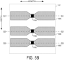
- FIG. 5A is a planar top-down view of the interface 106, with the sensors 110A-C removed.
- each of the through-holes 407A-C is centered on an axis A-A.
- one or more of the through-holes 407A-C are offset from axis A-A.
- one of the through-holes 407A-C may be situated to the left of axis A-A and another one of the through-holes 407A-C may be situated to the right of axis A-A.
- each of the notches 401A-B is centered on axis A-A.
- one or more of the notches 401A-B are offset from axis A-A to accommodate the placement of additional hardware on the PCB 107.
- one of the notches 401A-B may be formed to the left of axis A-A and the other one of the notches 401A-B may be formed to the right of axis A-A.
- notch 401A has the same size and shape as notch 401B.
- notch 401A has a different size and/or shape than notch 401B.
- each of the notches 403A-B is centered on axis A-A.
- one or more of the notches 403A-B are offset from axis A-A to accommodate the placement of additional hardware on the PCB 107.
- one of the notches 403A-B may be formed to the left of axis A-A and the other one of the notches 403A-B may be formed to the right of axis A-A.
- notch 403A has the same size and shape as notch 403B.
- notch 403A has a different size and/or shape than notch 403B.
- each of the notches 405A-B is centered on axis A-A.
- one or more of the notches 405A-B are offset from axis A-A to accommodate the placement of additional hardware on the PCB 107.
- one of the notches 405A-B may be formed to the left of axis A-A and the other one of the notches 405A-B may be formed to the right of axis A-A.
- notch 405A has the same size and shape as notch 405B.
- notch 405A has a different size and/or shape than notch 405B.
- providing the notches 401-405 on the conductors 108A-C, respectively, may help reduce cross-talk interference between neighboring ones of the conductors 108A-C.
- Cross talk between two neighboring conductors 108 may occur when the sensor 110 that is mounted over one of the conductors 108 senses a magnetic field that is generated by the other conductor 108.
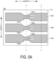
- FIG. 5B is a planar top-down view of the interface 106, with the sensors 110A-C present.
- the sensor 110A may have an axis of maximum sensitivity S1-S1 that is substantially perpendicular to the length and width of the conductor 108A.
- the sensor 110B may have an axis of maximum sensitivity S2-S2 that is substantially perpendicular to length and width of the conductor 108B.
- the sensor 110C may have an axis of maximum sensitivity S3-S3 that is substantially perpendicular to length and width of the conductor 108C.
- substantially perpendicular shall mean “within 5 degrees of being perpendicular.” It will be understood that the present disclosure is not limited to any specific orientation of the axis of maximum sensitivity of any of the sensors 110A-C for as long as the sensor is able to sense the level of the current flowing through its respective conductor 108.
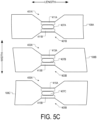
- FIG. 5C is a partial planar top-down view of the conductors 108A-C, according to aspects of the disclosure.
- through-hole 407A (and optionally the notches 401A-B) may define legs 411A and 411B in the conductor 108A.
- Legs 411A-B are denoted by dashed rectangles in FIG. 5C .
- Legs 411A and 411B according to the present example, have the same width. However, alternative implementations are possible in which leg 411A has a different width than leg 411B.
- the distance between legs 411A and 411B may be selected, such that it is large enough to avoid the creation of eddy currents between the legs 411A and 411B, while ensuring that the coupling coefficient K(f) between the legs 411A-B and the sensor 110 is large enough to meet the specification of the sensor 110A for reliable operation.
- decreasing the width of the conductor 108A by forming legs 411A-B may help reduce the variability of the coupling coefficient K(f) with respect to the frequency of the current that is carried over the conductor 108A.
- Through-hole 407B may define legs 413A and 413B in the conductor 108B.
- Legs 413A-B are denoted by dashed rectangles in FIG. 5C .
- Legs 413A and 413B according to the present example, have the same width. However, alternative implementations are possible in which leg 413A has a different width than leg 413B.
- the distance between legs 413A and 413B may be selected, such that it is large enough to avoid the creation of eddy currents between the legs 413A and 413B, while ensuring that the coupling factor K(f) between the legs 413A-B and the sensor 110B is large enough to meet the specification of the sensor 110B for reliable operation.
- decreasing the width of the conductor 108B by forming legs 413A-B may help reduce the variability of the coupling coefficient K(f) with respect to the frequency of the current that is carried over the conductor 108B.
- Through-hole 407C may define legs 415A and 415B in the conductor 108C.
- Legs 415A-B are denoted by dashed rectangles in FIG. 5C .
- Legs 415A and 415B according to the present example, have the same width. However, alternative implementations are possible in which leg 415A has a different width than leg 415B.
- the distance between legs 415A and 415B may be selected, such that it is large enough to avoid the creation of eddy currents between the legs, while ensuring that the coupling factor K(f) between legs 415A-B and the sensor 110C is large enough to meet the specification of the sensor 110C for reliable operation.
- decreasing the width of the conductor 108C by forming legs 415A-B may help reduce the variability of the coupling coefficient K(f) with respect to the frequency of the current that is carried over the conductor 108C.
- T is the thickness of any of conductors 108A-C.
- the thickness of the conductor 108 may be equal to the sum of the thicknesses of the conductor's constituent layers.
- the thickness of each 108A-C may be a dimension that is perpendicular to both of dimensions NL and W.
- Equation 3 illustrates that introducing a respective through-hole in each of the conductors 108A-C to form two separate legs results in a smaller increase in resistance of the conductors 108A-C in comparison to similar techniques that rely solely on notching.
- FIGS. 6A-B illustrate an example of the conductor 108A, in accordance with an alternative implementation.
- FIGS. 6A-B illustrate that in some implementations, the conductor 108A may include only one notch ( e.g ., notch 401).
- FIGS. 6A-B show the conductor 108A only, it will be understood that in some implementations, any or all of conductors 108B-C may have the same configuration.
- FIGS. 7A-B illustrate an example of the conductor 108A, in accordance with an alternative implementation.
- FIGS. 7A-B illustrate that in some implementations the conductor 108A may be provided with an additional through-hole 707A, as well as an additional sensor 710A that is mounted over the through-hole 707A.
- the sensor 710A may be the same or similar to the sensor 110A.
- the sensor 710A may have a function that is redundant to that of the sensor 110A and it may be provided to increase the reliability of the interface 106.
- the sensor 710A may be provided to achieve a higher Automotive Safety Integrity Level (ASIL) rating of the interface 106.
- ASIL Automotive Safety Integrity Level
- the through-holes 407A and 707A are centered on an axis B-B, which extends along the width W of the conductor 108A.
- at least one of the through-holes 407A and 707B is offset from the axis B-B.
- through-hole 407A may be formed to the left of axis B-B and through-hole 707A may be formed to the right of axis B-B.
- through-holes 407A and 707A are the same size and shape.
- the through-holes 407A and 707A have different shapes and/or sizes.
- FIGS. 7A-B show the conductor 108A only, it will be understood that in some implementations, any or all of conductors 108B-C may have the same configuration.
- FIGS. 8A-B illustrate an example of the conductor 108A, in accordance with an alternative implementation.
- FIGS. 8A-B illustrate that in some implementations, the notches 401A and 401B of the conductor 108A may have different shapes and sizes.
- FIGS. 8A-B show the conductor 108A only, it will be understood that in some implementations, any or all of conductors 108B-C may have the same configuration.
- FIGS. 9A-B illustrate an example of the conductor 108A, in accordance with an alternative implementation.
- FIGS. 9A-B illustrate that in some implementations, the notches 401A and 401B of the conductor 108A may be spaced apart from one another along the length L of the conductor 108A. This is in contrast to the preceding examples, in which the notches 401A-B are spaced apart from one another along the width of the conductor 108A.
- FIGS. 9A-B show the conductor 108A only, it will be understood that in some implementations, any or all of conductors 108B-C may have the same configuration. In the example of FIGS.
- the sensor 110A may have an axis of maximum sensitivity that is perpendicular (or otherwise transverse) to the length L and width W of the conductor 108A.
- the configuration shown in FIGS. 9A-B may prevent the sensor 110A from sensing magnetic field(s) generated by neighboring conductor(s).
- arranging the sensor 110A in the manner shown in FIGS. 9A-B may help reduce crosstalk between the sensor 110A and neighboring conductors ( e.g ., the conductors 110B-C, etc. ) .
- the present disclosure is not limited to any specific orientation of the axis of maximum sensitivity of the sensors 110A for as long as the sensor is able to sense the level of the current flowing through conductor 108A.
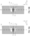
- FIG. 10A is a cross-sectional side view of the interface 106 that is taken along axis T-T (shown in FIG. 5A ).
- the conductor 108A includes a plurality of metal layers 1002 that are separated from each other by layers of dielectric material 1004.
- Each of the metal layers 1002 may have the same width W as the rest of the metal layers 1002.
- alternative implementations are possible in which at least two of the metal layers 1002 have different widths.
- each of the metal layers 1002 has the same thickness.
- alternative implementations are possible in which at least two of the metal layers 1002 have different thicknesses.
- the metal layers 1002 are situated directly over one another, such that none of the metal layers 1002 overhangs another one of the metal layers 1002.
- alternative implementations are possible in which at least one of the metal layers 1002 overhangs another one of the metal layers 1002. ( e.g., see FIG. 10C ).
- each of the metal layers 1002 has a main surface that are substantially parallel to the main surface 406 of the PCB 107.
- FIG. 10B is a cross-sectional side view of the interface 106 that is taken along axis A-A (shown in FIG. 5A ).
- FIG. 10B illustrates that the through-hole 407A may extend through all metal layers of the conductor 108A.
- FIG. 10B further illustrates that the through-hole 407A may be filled with a dielectric material.
- FIG. 10C shows an example of the conductor 108A, in accordance with an alternative implementation. More particularly, FIG. 10C is a cross-sectional side view of the conductor 108A that is taken along axis A-A (shown in FIG. 5A ).
- leg 411A is formed of metal layers 1002A-E. As illustrated, each of the metal layers 1002A-E may be formed in a different plane. At least some of the metal layers 1002A-E may have a different width and they may overhang one another, as shown.
- metal layers 1002B-1002E are integral metal layers and metal layer 1002A is a segmented metal layer.
- Metal layer 1002A may include a plurality of segments 1003 that are separated from one another by the dielectric material (which is also used to separate the metal layers 1002A-E). Each of the segments 1003 may have a width that is smaller than a width of the metal layer 1002E and/or the width of one or more of the metal layers 1002B-D.
- leg 411B is formed of metal layers 1002F-J.
- each of the metal layers 1002F-J may be formed in a different plane.
- Each of the metal layers may be formed of a conductive material (e.g ., metal).
- at least some of the metal layers 1002 F-J may have a different width and they may overhang one another, as shown.
- metal layers 1002F-G and 1002I-J are integral metal layers and metal layer 1002H is a segmented metal layer.
- Metal layer 1002H may include a plurality of segments 1005 that are separated from one another by the dielectric material (which is also used to separate the metal layers 1002F-J).
- Each of the segments 1005 may have a width that is smaller than the width of the metal layer 1002E and/or the width of one or more of the metal layers 1002B-D.
- the remaining portions of the conductor 108A also have the configuration shown in FIG. 10C .
- FIG. 10C shows the conductor 108A only, it will be understood that in some implementations, any of conductors 108B-C may have the same configuration.
- FIG. 10D shows an example of the conductor 108A, in accordance with an alternative implementation. More particularly, FIG. 10D is a cross-sectional side view of the conductor 108A that is taken along axis A-A (shown in FIG. 5A ).
- leg 411A is formed of metal layers 1002 (depicted as solid black rectangles).
- the metal layers 1002 may be partially separated by layers of dielectric material that are disposed between the metal layers 1002.
- the metal layers 1002 may be electrically coupled to one another by conductive vias 1008 that are formed in the ends of the metal layers 1002, and which are depicted as cross-hatched rectangles.
- Leg 411B is similarly formed of metal layers 1002 (depicted as solid black rectangles).
- the metal layers 1002 may be partially separated by layers of dielectric material that are disposed between the metal layers 1002.
- the metal layers 1002 may be electrically coupled to one another by conductive vias 1008 that are formed in the ends of the metal layers 1002, and which are depicted as cross-hatched rectangles.
- the remaining portions of the conductor 108A also have the configuration shown in FIG. 10D .
- FIG. 10D shows the conductor 108A only, it will be understood that in some implementations, any of conductors 108B-C may have the same configuration.
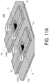
- FIGS. 11A-B show a perspective view of an example of a system 1100, according to aspects of the disclosure.
- the system may include conductors 1104A-B that are disposed over a printed circuit board (printed circuit board) 1102.
- Conductor 1104A may include a through-hole 1106A
- conductor 1104B may include a through-hole 1106B.
- a current sensor 1108A may be disposed inside the through-hole 1106A and used to measure an electrical current through the conductor 1104A.
- the current sensor 1108A may be the same or similar to the current sensor 110, which is discussed above with respect to FIG. 2 .
- a current sensor 1108B may be disposed inside the through-hole 1106B and used to measure an electrical current through the conductor 1104B.
- the current sensor 1108B may be the same or similar to the current sensor 110, which is discussed above with respect to FIG. 2 .
- conductor 1104A has a longitudinal axis A1-A1
- conductor 1104B has a longitudinal axis A2-A2 that is substantially parallel to the axis A1-A1
- the system 1100 has an axis B-B that is substantially perpendicular to the longitudinal axes A1-A1 and A2-A2.
- current sensors 1108A-B may be aligned with the axis B-B.
- magnetic field sensing elements 1114A and 1116A which are part of current sensor 1108A, may be aligned with the axis B-B.
- a disadvantage of this configuration is that it suffers from high crosstalk between the current sensor 1108A and the conductor 1104B.
- FIG. 11B shows that magnetic field sensing element 1116A is closer to conductor 1104B than magnetic field sensing element 1114A.
- the magnetic field (or magnetic flux density) generated by conductor 1104B is greater on magnetic field sensing element 1116A than magnetic field sensing element 1114A.
- the accuracy of the current sensor 1108A may be reduced.
- FIGS. 12A-24B shows alternative configurations that address the disadvantages of the configuration of FIGS. 11A-B .
- Each of the configurations discussed with respect to any of FIGS. 12A-24B is advantageous because, in comparison to the configuration of FIGS. 11A-B , it exhibits reduced crosstalk between current sensors and adjacent conductors, which in turn may help increase the accuracy of the current sensors.
- the conductors shown in FIGS. 11A-24B may be used to deliver power from a power source to a power load, such as an electrical motor and/or any other suitable power load.
- the current sensors that are disposed inside the conductors may be used to measure the current through the conductors and their output may be utilized in various automated control algorithms that are used to operate the power load.
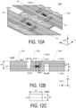
- FIG. 12A is a diagram of an example of a system 1200, according to aspects of the disclosure.
- system 1200 may include a printed circuit board 1201, a conductor 1202A, and a conductor 1202B.
- Conductor 1202A may include notches 1206A and 1208A, and a through-hole 1204A.
- each of notches 1206A and 1208A may be a void that is formed in one of the sides of conductor 1202A by removing material from conductor 1202A (e.g., by cutting or stamping out portions of conductor 1202A, etc .).
- the through-hole 1204A may be situated between the notches 1206A and 1208A, as shown.
- a current sensor 1210A may be positioned inside the through-hole 1204A.
- the current sensor 1210A may be arranged to measure the level of electrical current through conductor 1202A.
- the current sensor 1210A may be coupled to one or more conductive traces in the printed circuit board 1201 and arranged to send and receive signals via the conductive traces.
- Each of the current sensors 1210A-B may be the same or similar to the current sensor 110, which is discussed above with respect to FIG. 2 .
- Conductor 1202B may include notches 1206B and 1208B, and a through-hole 1204B.
- each of notches 1206B and 1208B may be a void that is formed in one of the sides of conductor 1202B by removing material from conductor 1202B (e.g., by cutting or stamping out portions of conductor 1202A, etc .).
- the through-hole 1204B may be situated between the notches 1206A and 1208A, as shown.
- a current sensor 1210B may be positioned inside the through-hole 1204B.
- the current sensor 1210B may be arranged to measure the level of electrical current through conductor 1202B.
- the current sensor 1210B may be coupled to one or more conductive traces in the printed circuit board 1201 and arranged to send and receive signals via the conductive traces.
- each (or at least one of) conductor(s) 1202A and 1202B may be fully embedded or integrated into the printed circuit board 1201. Additionally or alternatively, in some implementations, each (or at least one of) conductor(s) 1202A and 1202B may be partially embedded or integrated into the printed circuit board 1201. Additionally or alternatively, in some implementations, each (or at least one of) conductor(s) 1202A and 1202B may be disposed above or below the printed circuit board 1201.
- an air gap may be provided between the conductors(s) 1202A and/or 1202B or the conductors 1202A and/or 1202B may be affixed to the printed circuit board 1201 via a layer of adhesive material that doubles as an electrical isolator.
- each of the current sensors 1210A-B has an axis of maximum sensitivity that is substantially parallel to the Z-axis of coordinate system 1273 (e.g ., an axis of maximum sensitivity that is substantially perpendicular to the printed circuit board 1201).
- each of the current sensors 1210A-B is provided in a system-in-package (SIP) package.
- SIP system-in-package
- the through-holes 1204A-B are made large enough, it is possible to provide the current sensors 1210A-B in a surface mount package (for as long as the axes of the sensing elements in the current sensors 1210A-B are substantially parallel to the Z-axis of coordinate system 1273).
- a SIP package would use a magnetic technology that has in-plane sensitivity (e.g ., vertical Hall, TMR, etc .) while a surface mount package would require a magnetic technology sensitive in a perpendicular direction (e.g ., planar Hall, magnetic flux concentrator + TMR etc .)
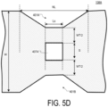
- FIG. 12B is a planar top-down view of conductor 1202A, according to aspects of the disclosure.
- conductor 1202A may have a central longitudinal axis A3-A3.
- the notch 1206A may have a length L1 and a width W1.
- the notch 1208A may have a length L2 and a width W2.
- the current sensor 1210A may include magnetic field sensing elements 1212A and 1214A. According to the present example, the magnetic field sensing elements 1212A and 1214A are aligned with the central longitudinal axis A3-A3. The distance from the center of magnetic field sensing element 1212A to edge 1216A of conductor 1202A is D2.
- the distance from the center of magnetic field sensing element 1212A to edge 1218A of conductor 1202A is D1.
- the distance from the center of magnetic field sensing element 1214A to edge 1216A of conductor 1202A is D2.
- the distance from the center of magnetic field sensing element 1214A to edge 1218A of conductor 1202A is D1.
- the distance D1 is equal to the distance D2.
- the magnetic field sensing elements 1212A and 1214A are not centered on the central longitudinal axis A3-A3, in which case the distance D1 may be different from the distance D2.
- the width W1 is such that the notch 1206A extends past the central longitudinal axis A3-A3 ( i.e. , W1>D2).
- the width W2 is such that the notch 1208A extends past the central longitudinal axis A3-A3 (i.e. , W2>D1).
- the width W1 is equal to the width W2.
- the widths W1 and W2 are different.
- the length L1 is equal to the length L2.
- alternative implementations are possible in which the lengths L1 and L2 are different.
- FIG. 12C is a diagram of the through-hole 1204A.
- the through-hole 1204A may have a length L3 and a width W3.
- the length L3 is greater than the width W3, so that the through-hole 1204A has an elongated shape that extends lengthwise in the conductor 1202A.
- the length L3 is equal to the width W3 or is smaller than the width W3.
- the length L3 is greater than the lengths L1 and L2.
- the width W3 is smaller than the widths W1 and W2.
- the width W3 is greater than or equal to at least one of the widths W1 and W2.
- notches 1206A and 1208A divide conductor 1202A into portions 1232, 1234, and 1236 (shown in FIG. 12B ).
- FIG. 12D shows portion 1234 in further detail.
- portion 1234 may include a leg 1242 and a leg 1244.
- Leg 1242 may have a width W4 and leg 1244 may have a width W5.
- each of the widths W4 and W5 is smaller than the full width W6 of conductor 1202A.
- widths W4 and W5 are equal.
- portion 1234 may include legs 1246 and 1248.
- Leg 1246 may have a width W7 and leg 1248 may have a width W8.
- width W7 is the same as width W8, however alternative implementations are possible in which width W7 is greater than or is smaller than width W8.
- width W7 is the same as widths W4 and W5.
- width W7 is smaller or greater than at least one of widths W4 and W5.
- making the legs 1246 and 1248 narrow i.e. , using small widths W7 and W8 focuses the electrical current through the conductor 1202A in a small section of the conductor 1202A thus increasing the current density close to the sensor 1210A, which is placed in the aperture 1204A of the conductor 1202A. This results in a larger magnetic field being generated by the current, which in turn results in increased accuracy of the sensor 1210.
- the through-hole 1204A is shaped as a rectangle, and includes edges 1286 and 1288 that are substantially parallel to the central longitudinal axis A3-A3.
- the edges 1286-1288 are oriented at an angle relative to the central longitudinal axis A3-A3.
- the through-hole 1204A may be shaped as a rectangle or another type of parallelogram.
- the angle between each of edges 1286 and 1288 and axis A3-A3 may be in the range of 30-75 degrees. Additionally, or alternatively, in some implementations, the angle may be substantially equal to 45 degrees.
- the through-hole 1204A is shaped as a rectangle, the present disclosure is not limited to any specific shape for the through-hole 1204A.
- the through-hole may be shaped as an oval, a circle, a trapezoid, a parallelogram, a polygon, etc.
- FIG. 12E shows a cross-sectional side view of the conductor 1202A, according to aspects of the disclosure.
- the current sensor 1210A may include terminals 1268A.
- Each of terminals 1268A may be coupled to a respective conductive trace that is part of the printed circuit board 1201 (not shown).
- the magnetic field sensing elements 1212A and 1214A may be disposed inside the through-hole 1204A, such that magnetic field sensing elements 1212A and 1214 are situated below a top (and/or main) surface 1262A of conductor 1202A and above a bottom (and/or main) surface 1264A of conductor 1202A.
- each of the magnetic field sensing elements 1212A and 1214A may have a respective axis of maximum sensitivity that is substantially parallel to the Z-axis of coordinate system 1273.
- the magnetic field sensing elements 1212A and 1214A are aligned with an alignment axis G-G.
- the alignment axis is coincidental with the central longitudinal axis A3-A3 ( i.e., it is the same axis).
- the alignment axis G-G is different, but parallel, to the central longitudinal axis A3-A3; in such implementations, the alignment axis G-G may be a longitudinal axis of the conductor 1202A, other than a central longitudinal axis.
- the alignment axis G-G may be oriented at an angle relative to the central longitudinal axis A3-A3. In such implementations, the angle may be in the range of 30-75 degrees, etc. Additionally or alternatively, in some implementations, the angle may be substantially equal to 45 degrees.
- the alignment axis G-G may be substantially parallel to the central longitudinal axis A4-A4 of conductor 1202A (shown in FIG. 12A ) irrespective of whether the central longitudinal axes A3-A3 and A4-A4 are substantially parallel to one another.
- making the alignment axis G-G parallel to the central longitudinal axis A4-A4 of conductor 1202B would make sensing elements 1212A and 1214A equidistant from conductor 1202B, which in turn may reduce, or ideally eliminate, crosstalk between conductor 1202B and the sensor 1010A.
- the conductor 1202A may have a thickness T in the range of 1-10mm. However, the present disclosure is not limited to any specific thickness for the conductor 1202A.
- FIG. 12F shows a planar top-down view of the conductor 1202A.
- electrical current may flow from end 1291 to end 1292.
- End 1291 may extend between end-corners 1293 and 1294 of conductor 1202A.
- End 1292 may extend between end corners 1295 and 1296. Together, end-corners 1293-1296 define a rectangle 1299.
- the central longitudinal axis A3-A3 may intersect end 1291 at point P1, which is equidistant from end-corners 1293 and 1294.
- the central longitudinal axis A3-A3 may intersect end 1292 at point P2, which is equidistant from end corners 1295 and 1296.
- the central longitudinal axis of a conductor extends in the direction of the flow of current through the conductor and it intersects the conductor at a location that is equidistant from adjacent end corners of the conductor.
- a longitudinal axis of the conductor may be parallel to the central longitudinal axis, but it may or may not intersect the conductor at locations that are equidistant from adjacent end corners of the conductor.
- the general outline of side-edge 1298 of the conductor 1202A as illustrated by a dashed line representing the side of rectangle 1299, is parallel to the central longitudinal axis A3-A3.
- the general outline of side-edge 1297 of the conductor 1202A is parallel to the central longitudinal axis A3-A3.
- the magnetic field sensing elements 1212A and 1214A may be aligned with the central longitudinal axis A3-A3 of the conductor 1202A.
- the central longitudinal axis A3-A3 of conductor 1202A is substantially parallel to the central longitudinal axis A4-A4 of conductor 1202B and/or the side edges of conductor 1202B.
- the magnetic field sensing elements 1212A and 1214A are spaced apart by the same distance from conductor 1202B. This causes magnetic field sensing elements 1212A and 1214A to be subjected to same magnetic field (or magnetic flux) originating from conductor 1202B.
- the phrase "a pair of magnetic field sensing elements are aligned with a given axis” shall mean that each of the magnetic field sensing elements is disposed on the axis, directly above the axis, or directly below the axis, when the axis lies in the X-Y plane of coordinate system 1273. It will be appreciated that under this definition, the pair of magnetic field elements would be considered aligned with the axis even if one of the magnetic field sensing elements is disposed on the axis and the other one is disposed above or below the axis, etc.
- the phrase “substantially equal to X degrees” (where X is an integer) shall mean within +/- 10 degrees of X.
- the phrase substantially parallel shall mean "within +/- 10 degrees of being exactly parallel.”
- the phrase “substantially perpendicular” shall mean within +/- 10 degrees of being exactly perpendicular.
- the notches 1206A and 1208A each have a rectangular shape
- the present disclosure is not limited thereto.
- at least one of the notches 1206A and 1208A may have a triangular shape, an oval shape, a trapezoidal shape, a curved shape, and/or any other suitable type of shape.
- each of the notches 12A-F has sharp corners
- alternative implementations are possible in which at least one of the notches 12A-F has rounded corners.
- the conductor 1202A-F includes two notches ( i.e ., notches 1206A and 1208A)
- alternative implementations are possible in which the conductor 1202A includes only one notch or more than two notches, etc.
- FIGS. 12A-F show an example of one possible implementation of conductor 1202A.
- conductor 1202B may have identical or similar configuration to that of conductor 1202A.
- the current sensor 1210B may identical configuration to that of current sensor 1210A.
- the current sensor 1210B (or its magnetic field sensing elements) may have the same or similar positioning (or orientation) relative the conductor 1202B as the sensor 1210A has relative to conductor 1202A.
- the concepts and ideas that are expressed with respect to the configuration of conductor 1202A apply in equal force to conductor 1202B, as well.
- FIGS. 12A-D show an example of one possible implementation of conductor 1202A.
- the discussion that follows with respect to FIGS. 13-16 provides examples of different variations that can be applied to the implementation of conductor 1202A that is presented in FIGS. 12A-F .
- FIG. 13A shows the conductor 1202A in accordance with another implementation.
- the through-hole 1204A is shaped as a parallelogram.
- legs 1242 and 1244 each have a trapezoidal shape, while legs 1246 and 1248 each have a rectangular shape.
- magnetic field sensing elements 1212A and 1214A are disposed on the central longitudinal axis A3-A3 of the conductor 1202A.
- FIG. 13B shows the conductor 1202A in accordance with yet another implementation.
- the through-hole 1204A is shaped as a parallelogram.
- legs 1242 and 1244 each have a trapezoidal shape, while legs 1246 and 1248 each have a rectangular shape.
- magnetic field sensing elements 1212A and 1214A are disposed on axis S-S, which runs substantially in parallel to edges 1312 and 1314 of the through-hole 1204A.
- axis S-S is equidistant from edges 1312 and 1314.
- alternative implementations are possible in which axis S-S is closer to one of edges 1312 and 1314 than the other.
- FIG. 14 shows the conductor 1202A in accordance with yet another implementation.
- the length L1 of notch 1206A is greater than the length L2.
- the width W2 of notch 1208A is greater than the width W1 of notch 1206A.
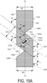
- FIGS. 15A-B show the conductor 1202A in accordance with yet another implementation.
- notches 1208A and 1206A are shaped in such a way so as to cause portion 1234 to extend at an angle relative to portions 1232 and 1236.
- notches 1206A and 1208A each have a triangular shape.
- portion 1234 has an axis T-T that is arranged at an angle ⁇ relative to the central longitudinal axis A3-A3 of conductor 1202A.
- Edge 1508 of through-hole 1204A may be substantially parallel to edge 1512 of notch 1208A.
- Edge 1510 of through-hole 1204A may be substantially parallel to edge 1514 of notch 1206A.
- Edges 1508 and 1510 may both be substantially parallel to the central axis T-T.
- Magnetic field sensing elements 1212A and 1214A of current sensor 1210A may be aligned with an axis G-G.
- axis G-G is perpendicular to the central axis T-T.
- alternative implementations are possible in which axis G-G is orientated relative to axis T-T at an angle other than 90 degrees.
- the axis G-G is arranged at an angle ⁇ relative to axis A3-A3.
- the angle ⁇ may be less than 75 degrees or in the range of 30-75 degrees.
- magnetic field sensing elements 1212A and 1214A are aligned on the central longitudinal axis A3-A3.
- portion 1234 may have a width W17.
- width W17 is greater than the full width W6 of conductor 1202A.
- the width W17 is smaller than or equal to the width W6.
- portion 1234 may have legs 1522 and 1524.
- Leg 1522 may have a width W18 and leg 1524 may have a width W19.
- widths W19 and W18 are smaller than the width W6 of the portions 1232 and 1236.
- widths W18 and W19 are equal.
- the angle ⁇ is equal to 45 degrees.
- alternative implementations are possible in which the angle ⁇ is less than 75 degrees or in the range of 30-75 degrees.
- the current sensor 1210A is not completely immune from cross-talk with conductor 1202B. However, because the current sensor 1210A is rotated by 45 degrees (from the 90-degree configuration of FIGS. 11A-B ), the effects of crosstalk with conductor 1202B on the current sensor 1210A would still be reduced by 50%. At the same time, the orientation of current sensor 1210A that is shown in FIG. 15 results in a higher magnetic flux being incident on magnetic field sensing elements 1212A and 1214A than the orientation of current sensor 1210A that is shown in FIGS. 12A-F . This in turn may positively affect the accuracy of the current sensor 1210A, under some circumstances.
- FIGS. 11A-B has a high signal strength and a high cross-talk
- the configuration of FIGS. 12A-F has a lower signal strength and low crosstalk
- the configuration of FIG. 15 represents a compromise between the former two configurations by featuring higher signal strength that the configuration of FIGS. 12A-F and a lower cross-talk than the configuration of FIGS. 11A-B .
- FIG. 16 shows the conductor 1202A in accordance with yet another implementation.
- the through-hole 1204A is omitted from the conductor 1202A, and the current sensor 1210A is disposed in the notch 1206A.
- the notch 1206A may have an axis M-M that runs through its middle of notch 1206A and is perpendicular to the central longitudinal axis A3-A3.
- the current sensor 1210A may be disposed on the side of the axis M-M.
- the current sensor 1210A is centered on the axis M-M, such that magnetic field sensing elements 1212A and 1214A are disposed on opposite sides of the axis M-M.
- the axis M-M may also be referred to as "the median axis" of notch 1206A.
- placing the sensor 1210A on the side of the median axis M-M is advantageous because it would bring the sensor 1210A closer to the source of the magnetic field that is being measured by the sensor 1210A. As a result, the sensor 1210A would be able to sense a larger field from the same amount of current.
- the magnetic field source is leg 1601 of conductor 1202A.
- FIG. 17 is a diagram of an example of a system 1700, according to aspects of the disclosure.
- the system 1700 may include a conductor assembly 1701 and a sensor assembly 1705 that is inserted in an aperture 1703 (e.g., a through-hole, etc .) that in the conductor assembly 1701.
- the conductor assembly 1701 may have a longitudinal axis A5-A5.
- the aperture 1703 may include a longitudinal axis Q-Q.
- the longitudinal axis Q-Q of the aperture may be substantially perpendicular to the longitudinal axis Q-Q.
- the conductor assembly may include a plurality of conductors 1706 that are spaced apart by layers of dielectric material 1708.
- the conductors 1706 are electrically isolated from one another by the layers of dielectric material 1708.
- the layers of dielectric material may be omitted, while leaving an air gap between any two adjacent conductors 1706.
- the conductors 1706 may be electrically isolated from one another by air, rather than the provision of layers of dielectric material between them.
- the aperture 1703 may be formed by aligning respective through-holes that are formed in each of the conductors 1706.
- the sensor assembly 1705 may include a printed circuit board 1702 and a plurality of current sensors 1704. Each of the current sensors 1704 may be the same or similar to the current sensor 110, which is discussed above with respect to FIG. 2 . Each of the current sensors 1704 may have an axis of maximum sensitivity that is substantially parallel to central-longitudinal axis Q-Q of the aperture 1703. The axis of maximum sensitivity may be perpendicular to the central longitudinal axis A5-A5 of the conductor assembly 1701. The central longitudinal axis A5-A5 may be parallel to each (or at least one) of the central longitudinal axes of the individual conductors 1706 that make up the conductor assembly 1701.
- Each of the current sensors 1704 may be configured to measure the electrical current through a different one of the conductors 1706.
- Each of the current sensors 1704 may be coupled to one or more conductive traces (not shown) in the printed circuit board 1702.
- the printed circuit board 1702 may further include an interface 1710.
- the interface 1710 may include one or more terminals. Each of the terminals in the interface 1710 may be coupled to a respective one of the current sensors 1704 via a respective conductive trace that is formed in the printed circuit board 1702.
- the interface 1710 may be used by external circuitry to send and receive data from the current sensors 1704. In the example of FIG.
- the central longitudinal axis A5-A5 may extend in parallel with the Z-axis of the coordinate system 1723
- arm portion 1802 of printed circuit board 1702 extends in parallel with the Y-axis of the coordinate system 1723
- cross-portion 1804 of printed circuit board 1702 extends in parallel with the X-axis of the coordinate system 1723
- the longitudinal axis Q-Q of the aperture 1703 may extend in parallel with the Y axis of the coordinate system 1723.
- FIG. 18 is a perspective view of the sensor assembly 1705, according to aspects of the disclosure.
- the printed circuit board 1702 may be T-shaped, and as such, it may include an arm portion 1802 and a cross-portion 1804.
- the arm portion 1802 may be inserted in the aperture 1703 of the conductor assembly 1701, while the cross-portion 1804 engages an exterior surface of the conductor assembly 1701 so as to prevent the sensor assembly 1705 from sinking any further into the aperture 1703.
- the printed circuit board 1702 may be so dimensioned as to ensure that when the cross-portion 1804 comes in contact with the conductor assembly 1701, each of the current sensors 1704 would be situated in the respective through-hole 2202 (shown in FIG. 22 ) of a different one of the conductors 1706.
- the arm portion 1802 and cross-portion 1804 of the printed circuit board 1702 may be so dimensioned as to ensure a proper alignment between the current sensors 1704 and the conductors 1706.
- FIG. 19A is a planar side view of the system 1700 when viewed from direction D1 (shown in FIG. 17 ).
- FIG. 19B is a planar side view of the system 1700 when viewed from direction D2 (shown in FIG. 17 ).
- FIGS. 19A-B illustrate that in some implementations the aperture 1703 may be a through hole.
- each of current sensors 1704 may include magnetic field sensing elements 1752 and 1754 that are situated on opposite sides of the central longitudinal axis A5-A5.
- each of magnetic field sensing elements 1752 and 1754 may have a respective axis of maximum sensitivity that is substantially perpendicular to the central longitudinal axis A5-A5.
- the axis of maximum sensitivity of each of the magnetic field sensing elements 1752 and 1754 may extend in parallel to the longitudinal axis Q-Q of the aperture 1703.
- the axis Q-Q is perpendicular to the axis A5-A5
- alternative implementations are possible in which the axis Q-Q is oriented at a different angle relative to the axis A5-A5.
- each current sensor 1704 may be aligned with a different respective axis D-D.
- Each respective axis D-D may be perpendicular to the central longitudinal axes A5-A5 of all conductors 1706 in the conductor assembly 1701.
- Each respective axis D-D may be perpendicular to the longitudinal axis Q-Q of the aperture 1703.
- the sensing elements 1754 and 1752 in the current sensor 1704 that is disposed in any given one of conductors 1706 may be equidistant from all remaining conductors 1706 in the conductor assembly 1701. As discussed above, this may in turn limit the amount of crosstalk between the current sensor 1704 and the remaining conductors 1706.
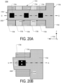
- FIG. 20A is a cross-sectional top-down view of the system 1700 that is taken along an axis T-T (shown in FIG. 17 ).
- FIG. 20 illustrates that when the sensor assembly 1705 is inserted in the aperture 1703, each of the current sensors 1704 may be disposed (at least in part) inside the respective through-hole 2202 of a different one of the conductors 1706.
- FIG. 20B is a partial cross-sectional top-down view of the system 1700 that is taken along an axis T-T (shown in FIG. 17 ).
- FIG. 20B illustrates that each of the conductors 1706 may have main surfaces 2026 and 2028 and each of the current sensors 1704 may include magnetic field sensing elements 1752 and 1754.
- magnetic field sensing elements are disposed between the main surfaces 2026 and 2028, and inside the through-hole 2022 of the conductor 1706.
- FIG. 20B is provided to illustrate the relative positioning of the magnetic field sensing elements of each of the current sensors 1704 relative to the current sensor's 1704 respective conductor 1706.
- FIG. 20B is provided to illustrate the relative positioning of the magnetic field sensing elements of each of the current sensors 1704 relative to the current sensor's 1704 respective conductor 1706.
- the magnetic field sensing elements 1752 and 1754 in each of the current sensors 1706 may be disposed on opposite sides of the axis Q-Q.
- the axis Q-Q runs through the center of the aperture 1703 and the aperture 1703 is fully symmetrical with respect to the axis QQ.
- each of conductors 1706 may include main surfaces 2026 and 2028 that are parallel to each other and edges 2281, 2283, 2285, and 2287 that are disposed between the main surfaces 2026 and 2028.
- each of the main surfaces 2026 and 2028 may have a much greater surface area than the edges 2281, 2283, 2285, and 2287. ( e.g., 5 times greater, 10 times greater, etc .).
- a main surface of each of the conductors 1706 is facing a main surface of another one of the conductors 1706. This is in contrast with the system 1200 (shown in FIG. 12 ) where the edges of conductors 1202A and 1202B are facing each other.
- FIG. 21A is perspective view of the conductor assembly 1701.
- FIG. 21B is a side view of the conductor assembly 1701 when viewed from direction D3.
- each of the conductors 1706 may be coupled to each other via the dielectric layers 1708.
- each conductor 1706 may be adhered to its neighboring dielectric layer(s) 1708 via a respective layer of adhesive material (not shown).
- the conductors 1706 are separated by dielectric layers 1708, alternative implementations are possible in which conductors 1706 are separated by air gaps. Stated succinctly, the present disclosure is not limited to any specific way of achieving electrical isolation between the conductors 1706 in conductor assembly 1701.
- FIG. 22A is a planar side view of a conductor 1706, according to aspects of the disclosure.
- conductor 1706 may have a central longitudinal axis A6-A6 that is parallel to the axis A5-A5 (shown in FIG. 17 ) of the conductor assembly 1701.
- the conductor 1706 may include portions 2212, 2214, and 2216, with the through-hole 2202 being formed in portion 2214.
- through-hole 2202 may define legs 2224 and 2226 of the conductor 1706.
- the current sensor 1704 may measure the level of electrical current through the legs 2224 and 2226.
- the conductor 1706 may have width W11.
- Leg 2224 may have a width W12 that is smaller than the width W11.
- Leg 2226 may have a width W13 that is smaller than the width W11.
- width W12 and W13 are equal.
- alternative implementations are possible in which the widths W12 and W13 are different.
- FIG. 22B is a planar side view of a dielectric layer 1708.
- the dielectric layer 1708 may include a through-hole 2232 that defines legs 2234 and 2236.
- FIG. 22B illustrates that when a plurality of conductors 1706 are interleaved with a plurality of dielectric layers 1708 to form the conductor assembly 1701, the respective through-hole 2232 of each of the dielectric layers 1708 may be aligned with the respective apertures of the conductors 1706.
- FIG. 22B illustrates that each dielectric layer 1708 may have the same or similar shape and dimensions as any of the conductors 1706.
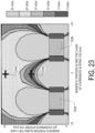
- FIG 23 is heatmap showing the magnetic flux density that is produced by a front conductor 1706 in the X-Y plane of the coordinate system 1723.
- the front conductor 1706 is the conductor 1706 that is disposed immediately next to the cross-portion 1804 of printed circuit board 1702 ( e.g ., see FIG. 17 .).
- the conductor that is disposed the furthest away from the cross-portion 1804, among the conductors 1706 in the conductor assembly 1701, is herein referred to as the "back conductor 1706".
- the conductor 1706 that is disposed between the back conductor 1706 and the front conductor 1706 is referred to as "the middle conductor 1706".
- the current sensor 1704 that is disposed inside the through-hole of the front conductor 1706 is herein referred to as “the front current sensor 1704"; the current sensor 1704 that is disposed inside the through-hole of the middle conductor 1706 is herein referred to as “the middle current sensor 1704"; and the current sensor 1704 that is disposed inside the through-hole of the middle conductor 1706 is herein referred to as “the middle current sensor 1704". It will be recalled that the front current sensor 1704 is disposed between legs 2224 and 2226 of the front conductor 1706.
- FIG. 23 shows that the configuration discussed with respect to FIGS. 17-24B is advantageous because it results in zero (or almost zero) cross-talk between the front conductor 1706 and the middle current sensor 1704 (because the magnetic field originating from the front conductor 1706 is near zero at the location of marker 2302).
- FIG. 23 also shows that the configuration discussed with respect to FIGS. 17-24 results in non-zero cross-talk between the front conductor 1706 and the back current sensor 1704. In this regard, it will be understood that the configuration discussed with respect to FIGS.
- the non-zero crosstalk between the front conductor 1706 and the back current sensor 1704 may be further curtailed by ensuring that the magnetic field sensing elements 1752 and 1754 in the back current sensor 1704 are equidistant from the front conductor 1706 ( e.g ., by aligning the magnetic field sensing elements 1752 and 1754 with an axis D-D, etc .) .
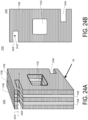
- FIGS. 24A is a perspective view of an alternative implementation of the conductor assembly 1701.
- FIG. 24B is a planar side view of the alternative implementation of conductor when viewed from direction D4.
- the conductors 1706 are identical (or similar) to the conductor 1202A, which is discussed above with respect to FIGS. 12B .
- FIGS. 24A-B are provided to illustrate that the present disclosure is not limited to the conductors 1706 having the shape shown in FIG. 22A . In this regard, it will be understood that each of conductors 1706 may have any of the shapes or configurations that are discussed above with respect to FIGS. 12A-16 .
- FIGS. 24A-B illustrate that when the conductors 1706 have notches, the notches may be aligned as well.
- a plurality of notches are aligned when a straight line, such as the line 2410, can pass through the interior of each of the notches without intersecting any of the conductors 1706.
- the conductor assembly 1701 includes an aperture 2402 and an aperture 2404.
- Aperture 2402 is formed by aligning respective first notches of the conductors 1706.
- Aperture 2404 is formed by aligning respective second notches of the conductors 1706.
- each of the first notches may correspond to notch 1208A (shown in FIG. 12B ) and each of the second notches may correspond to notch 1206A (also shown in FIG. 12B ).
- a computer program product e.g., in a non-transitory machine-readable storage medium such as, for example, a non-transitory computer-readable medium
- data processing apparatus e.g., a programmable processor, a computer, or multiple computers
- Each such program may be implemented in a high-level procedural or object-oriented programming language to work with the rest of the computerbased system.
- the programs may be implemented in assembly, machine language, or Hardware Description Language.
- the language may be a compiled or an interpreted language, and it may be deployed in any form, including as a stand-alone program or as a module, component, subroutine, or another unit suitable for use in a computing environment.
- a computer program may be deployed to be executed on one computer or multiple computers at one site or distributed across multiple sites and interconnected by a communication network.
- a computer program may be stored on a non-transitory machine-readable medium that is readable by a general or special purpose programmable computer for configuring and operating the computer when the non-transitory machine-readable medium is read by the computer to perform the processes described herein.
- the processes described herein may also be implemented as a non-transitory machine-readable storage medium, configured with a computer program, where upon execution, instructions in the computer program cause the computer to operate in accordance with the processes.
- a non-transitory machine-readable medium may include but is not limited to a hard drive, compact disc, flash memory, non-volatile memory, or volatile memory.
- the term unit e.g ., a addition unit, a multiplication unit, etc.
- the term unit may refer to hardware ( e.g ., an electronic circuit) that is configured to perform a function ( e.g ., addition or multiplication, etc. ), software that is executed by at least one processor, and configured to perform the function, or a combination of hardware and software.
- a magnetic field sensing element can include one or more magnetic field sensing elements, such as Hall effect elements, magnetoresistance elements, or magnetoresistors, and can include one or more such elements of the same or different types.
- Hall effect elements for example, a planar Hall element, a vertical Hall element, and a Circular Vertical Hall (CVH) element.
- magnetoresistance elements for example, a semiconductor magnetoresistance element such as Indium Antimonide (InSb), a giant magnetoresistance (GMR) element, for example, a spin valve, an anisotropic magnetoresistance element (AMR), a tunneling magnetoresistance (TMR) element, and a magnetic tunnel junction (MTJ).
- the magnetic field sensing element may be a single element or, alternatively, may include two or more magnetic field sensing elements arranged in various configurations, e.g., a half bridge or full (Wheatstone) bridge.
- the magnetic field sensing element may be a device made of a type IV semiconductor material such as Silicon (Si) or Germanium (Ge), or a type III-V semiconductor material like Gallium-Arsenide (GaAs) or an Indium compound, e.g., Indium-Antimonide (InSb).
- a type IV semiconductor material such as Silicon (Si) or Germanium (Ge)
- a type III-V semiconductor material like Gallium-Arsenide (GaAs) or an Indium compound, e.g., Indium-Antimonide (InSb).
Landscapes
- Physics & Mathematics (AREA)
- General Physics & Mathematics (AREA)
- Measuring Instrument Details And Bridges, And Automatic Balancing Devices (AREA)
Applications Claiming Priority (1)
| Application Number | Priority Date | Filing Date | Title |
|---|---|---|---|
| US18/300,776 US12352786B2 (en) | 2021-09-07 | 2023-04-14 | Current sensor system |
Publications (1)
| Publication Number | Publication Date |
|---|---|
| EP4450978A1 true EP4450978A1 (fr) | 2024-10-23 |
Family
ID=90482309
Family Applications (1)
| Application Number | Title | Priority Date | Filing Date |
|---|---|---|---|
| EP24166728.6A Pending EP4450978A1 (fr) | 2023-04-14 | 2024-03-27 | Système de capteur de courant |
Country Status (1)
| Country | Link |
|---|---|
| EP (1) | EP4450978A1 (fr) |
Citations (6)
| Publication number | Priority date | Publication date | Assignee | Title |
|---|---|---|---|---|
| US20120262152A1 (en) * | 2011-04-14 | 2012-10-18 | Udo Ausserlechner | Current sensors, systems and methods |
| US20150204919A1 (en) * | 2014-01-21 | 2015-07-23 | Hitachi Metals, Ltd. | Current detection structure |
| US20160223594A1 (en) * | 2013-09-05 | 2016-08-04 | Asahi Kasei Microdevices Corporation | Current Sensor |
| US10481181B2 (en) | 2017-04-25 | 2019-11-19 | Allegro Microsystems, Llc | Systems and methods for current sensing |
| US20210311136A1 (en) * | 2020-04-07 | 2021-10-07 | Allegro Microsystems, Llc | Current sensor system |
| US20230071087A1 (en) * | 2021-09-07 | 2023-03-09 | Allegro Microsystems, Llc | Current sensor system |
-
2024
- 2024-03-27 EP EP24166728.6A patent/EP4450978A1/fr active Pending
Patent Citations (6)
| Publication number | Priority date | Publication date | Assignee | Title |
|---|---|---|---|---|
| US20120262152A1 (en) * | 2011-04-14 | 2012-10-18 | Udo Ausserlechner | Current sensors, systems and methods |
| US20160223594A1 (en) * | 2013-09-05 | 2016-08-04 | Asahi Kasei Microdevices Corporation | Current Sensor |
| US20150204919A1 (en) * | 2014-01-21 | 2015-07-23 | Hitachi Metals, Ltd. | Current detection structure |
| US10481181B2 (en) | 2017-04-25 | 2019-11-19 | Allegro Microsystems, Llc | Systems and methods for current sensing |
| US20210311136A1 (en) * | 2020-04-07 | 2021-10-07 | Allegro Microsystems, Llc | Current sensor system |
| US20230071087A1 (en) * | 2021-09-07 | 2023-03-09 | Allegro Microsystems, Llc | Current sensor system |
Similar Documents
| Publication | Publication Date | Title |
|---|---|---|
| US12352786B2 (en) | Current sensor system | |
| WO2023038725A1 (fr) | Système de capteur de courant | |
| US10746821B2 (en) | Current sensor | |
| US20240412891A1 (en) | Multiple branch bus bar for coreless current sensing application | |
| JP5066579B2 (ja) | 磁気センサ及び磁気センサモジュール | |
| US10605835B2 (en) | Current sensor | |
| US11892476B2 (en) | Current sensor package | |
| CN107533089A (zh) | 电流传感器 | |
| US12487255B2 (en) | Current sensor system | |
| JP7215451B2 (ja) | 電流センサ及びその製造方法、電気制御装置、並びに電流センサの設計方法 | |
| WO2018100778A1 (fr) | Capteur de courant et unité de capteur de courant | |
| JP7070532B2 (ja) | 磁気センサ | |
| US12078662B2 (en) | Techniques for reducing an eddy current in a ground plane of a coreless sensor | |
| WO2010010872A1 (fr) | Capteur magnétique et module à capteur magnétique | |
| WO2019069500A1 (fr) | Capteur magnétique et capteur de courant | |
| US11543469B2 (en) | Current sensor, and electric control apparatus including the current sensor | |
| EP4450978A1 (fr) | Système de capteur de courant | |
| JP2015036636A (ja) | 電流センサ | |
| US12504448B2 (en) | Conductor design with improved cross-talk error | |
| US20240361404A1 (en) | Magnetic sensor | |
| US20260023137A1 (en) | Magnetic sensor and manufacturing method for the same | |
| US12578402B2 (en) | Magnetic sensor | |
| US20260023138A1 (en) | Magnetic sensor | |
| US20250377422A1 (en) | Magnetic sensor | |
| US20260043878A1 (en) | Magnetic sensor |
Legal Events
| Date | Code | Title | Description |
|---|---|---|---|
| PUAI | Public reference made under article 153(3) epc to a published international application that has entered the european phase |
Free format text: ORIGINAL CODE: 0009012 |
|
| STAA | Information on the status of an ep patent application or granted ep patent |
Free format text: STATUS: THE APPLICATION HAS BEEN PUBLISHED |
|
| AK | Designated contracting states |
Kind code of ref document: A1 Designated state(s): AL AT BE BG CH CY CZ DE DK EE ES FI FR GB GR HR HU IE IS IT LI LT LU LV MC ME MK MT NL NO PL PT RO RS SE SI SK SM TR |
|
| STAA | Information on the status of an ep patent application or granted ep patent |
Free format text: STATUS: REQUEST FOR EXAMINATION WAS MADE |
|
| 17P | Request for examination filed |
Effective date: 20250407 |