EP4451561A1 - Empfängerschaltung - Google Patents
Empfängerschaltung Download PDFInfo
- Publication number
- EP4451561A1 EP4451561A1 EP23168998.5A EP23168998A EP4451561A1 EP 4451561 A1 EP4451561 A1 EP 4451561A1 EP 23168998 A EP23168998 A EP 23168998A EP 4451561 A1 EP4451561 A1 EP 4451561A1
- Authority
- EP
- European Patent Office
- Prior art keywords
- sub
- receiver
- output
- receivers
- signal
- Prior art date
- Legal status (The legal status is an assumption and is not a legal conclusion. Google has not performed a legal analysis and makes no representation as to the accuracy of the status listed.)
- Pending
Links
Images



Classifications
-
- H—ELECTRICITY
- H03—ELECTRONIC CIRCUITRY
- H03G—CONTROL OF AMPLIFICATION
- H03G3/00—Gain control in amplifiers or frequency changers
- H03G3/001—Digital control of analog signals
-
- H—ELECTRICITY
- H04—ELECTRIC COMMUNICATION TECHNIQUE
- H04B—TRANSMISSION
- H04B1/00—Details of transmission systems, not covered by a single one of groups H04B3/00 - H04B13/00; Details of transmission systems not characterised by the medium used for transmission
- H04B1/06—Receivers
- H04B1/16—Circuits
-
- H—ELECTRICITY
- H03—ELECTRONIC CIRCUITRY
- H03F—AMPLIFIERS
- H03F1/00—Details of amplifiers with only discharge tubes, only semiconductor devices or only unspecified devices as amplifying elements
- H03F1/08—Modifications of amplifiers to reduce detrimental influences of internal impedances of amplifying elements
- H03F1/22—Modifications of amplifiers to reduce detrimental influences of internal impedances of amplifying elements by use of cascode coupling, i.e. earthed cathode or emitter stage followed by earthed grid or base stage respectively
- H03F1/223—Modifications of amplifiers to reduce detrimental influences of internal impedances of amplifying elements by use of cascode coupling, i.e. earthed cathode or emitter stage followed by earthed grid or base stage respectively with MOSFET's
-
- H—ELECTRICITY
- H03—ELECTRONIC CIRCUITRY
- H03F—AMPLIFIERS
- H03F3/00—Amplifiers with only discharge tubes or only semiconductor devices as amplifying elements
- H03F3/04—Amplifiers with only discharge tubes or only semiconductor devices as amplifying elements with semiconductor devices only
- H03F3/08—Amplifiers with only discharge tubes or only semiconductor devices as amplifying elements with semiconductor devices only controlled by light
- H03F3/082—Amplifiers with only discharge tubes or only semiconductor devices as amplifying elements with semiconductor devices only controlled by light with FET's
-
- H—ELECTRICITY
- H03—ELECTRONIC CIRCUITRY
- H03G—CONTROL OF AMPLIFICATION
- H03G3/00—Gain control in amplifiers or frequency changers
- H03G3/20—Automatic control
- H03G3/30—Automatic control in amplifiers having semiconductor devices
- H03G3/3084—Automatic control in amplifiers having semiconductor devices in receivers or transmitters for electromagnetic waves other than radiowaves, e.g. lightwaves
-
- H—ELECTRICITY
- H03—ELECTRONIC CIRCUITRY
- H03F—AMPLIFIERS
- H03F2200/00—Indexing scheme relating to amplifiers
- H03F2200/435—A peak detection being used in a signal measuring circuit in a controlling circuit of an amplifier
-
- H—ELECTRICITY
- H03—ELECTRONIC CIRCUITRY
- H03F—AMPLIFIERS
- H03F2200/00—Indexing scheme relating to amplifiers
- H03F2200/91—Indexing scheme relating to amplifiers the amplifier has a current mode topology
Definitions
- the present disclosure relates to receiver circuits, and in particular to receiver circuits that provide feed-forward automatic gain calibration.
- a receiver circuit comprising:
- such a receiver circuit can provide very fast feedforward calibration without requiring a large circuit overhead.
- the amplifiers and comparators of two or more of the sub-receivers are configured to apply different gain factors and/or threshold values such that the associated sub-receiver is configured to compare the received input-signalling with an effective threshold value that is based on the gain factor and threshold value. For example, based on the product of the gain factor and threshold value.
- the comparators of the two or more sub-receivers are configured to compare the amplifier-output-signal from its associated amplifier with the same threshold value, but with different effective threshold values that are based on different gain factors.
- the two or more amplifiers are provided in parallel such that their amplifier-input-terminals are connected together such that they receive the same amplifier-input-signal.
- the amplifiers of one or more of the sub-receivers are provided in series such that: the amplifier-input-terminal of the amplifier of the one or more of the sub-receivers is connected to the amplifier-output-terminal of the amplifier of another one of the sub-receivers.
- the amplifiers of two or more of the sub-receivers are configured to apply the same gain factor.
- the comparators of the sub-receivers are configured to compare the amplifier-output-signal from its associated amplifier with the same threshold value.
- the controller is configured to: for subsequent signal processing, disable one or more of the sub-receivers, but not the preceding-sub-receiver.
- the controller is configured to: for subsequent signal processing, disable one or more of the sub-receivers, but not:
- controller is configured to disable one or more of the sub-receivers, but not:
- the receiver circuit comprises an optical receiver circuit.
- the input of the peak detector that is provided by the second scaled output signal is disabled.
- each of the peak detector and the valley detector comprise one or more hold capacitors.
- Each of each of the peak detector and the valley detector may be configured to discharge their holding capacitors to track amplitude / offset changes.
- a method of calibrating a receiver circuit comprising:
- AGC Automatic Gain Control
- AGC systems can utilize closed-loop feedback topology to continuously adjust gain of a signal path to maintain a fixed output amplitude for different input signal amplitudes.
- loop stability can restrict gain control settling speed and can require some "dummy" signal, such as a message preamble.
- Open-loop AGC which can utilize feed-forward gain control, does not suffer from stability constraints and can demonstrate very fast gain settling speeds.
- such solutions can use an auxiliary path, can have a peak detector and / or an ADC (analogue-to-digital converter) to estimate signal amplitude and to control gain of the main signal path.
- IR infra-red
- DR dynamic range
- examples disclosed herein relate to a wireless receiver that utilizes multiple sub-receivers and re-uses them for the purpose of instant high-speed feedforward gain calibration.
- the receiver does not require auxiliary calibration circuits or a programmable / variable gain amplifier in the primary signal path. This is because all processing can be performed by multiple signal paths, which work in different ranges of signal amplitudes.
- FIG. 1 shows an example embodiment of a receiver circuit 100.
- the receiver circuit 100 includes a receiver-input-terminal 101 and a receiver-output-terminal 102.
- the receiver-input-terminal 101 receives input-signalling.
- the receiver-output-terminal provides output-signalling.
- the receiver circuit 100 can be calibrated such that it provides automatic gain control (AGC).
- ADC automatic gain control
- the topology that is shown in Figure 1 can be considered as a receiver topology that functions like a flash type ADC, which estimates at calibration the strength of the input-signalling at the receiver-input-terminal 101 and sets the gain that is applied by the receiver 100 for subsequent signal processing.
- the receiver 100 includes a plurality of sub-receivers 103a-103e. Although five sub-receivers 103a-103e are shown in Figure 1 , it will be appreciated that more or fewer sub-receivers can be included in other examples.
- Each of the sub-receivers 103a-103e compares the received input-signalling with a different effective threshold value in order to provide a digital sub-receiver-output-signal 104a-104e. In this way, a sub-receiver is triggered (i.e., it's digital sub-receiver-output-signal 104a-104c is set high in this example) when the input-signalling exceeds its associated effective threshold value.
- the different effective thresholds have weighted values in a sequence between a most significant value and a least significant value.
- the effective threshold values are multiplied by a factor of 2 as the sequence progresses.
- the sequence of effective threshold values can be implemented in different ways which can include them being particularly suitable for voltage or current values.
- the receiver 100 also includes a controller 105, which in Figure 1 is labelled with "FF-AGC" as it can be considered as applying a Feed-Forward Automatic Gain Control (FF-AGC) algorithm.
- FF-AGC Feed-Forward Automatic Gain Control
- the controller 105 can detect calibration-signalling at the receiver-input-terminal 101. Such calibration-signalling, and it's associated detection, can be implemented in any of a number of ways, as will be discussed below with reference to Figure 3 .
- the controller 105 processes the digital sub-receiver-output-signals 104a-104e in order to identify the sub-receiver 103a-103e with the most significant effective threshold value that is triggered by the calibration-signalling as a triggered-sub-receiver. It will be appreciated that because the sub-receivers 103a-103e apply different effective threshold values, the specific amplitude / value of the calibration-signalling can exceed some, but not all, of the effective threshold values. Indeed, the effective threshold values can be given values that correspond to the intended dynamic range of the receiver circuit 100 such that this is the case.
- Each of the plurality of sub-receivers includes an amplifier 106 and a comparator 107.
- Each amplifier 106 has an amplifier-input-terminal and an amplifier-output-terminal.
- the amplifier-output-terminal provides an amplifier-output-signal.
- the comparator 107 compares the amplifier-output-signal with a threshold value in order to provide the digital sub-receiver-output-signal.
- amplifiers 106 of the sub-receivers are connected to the receiver-input-terminal 101 in parallel with each other. In this way, the receiver-input-terminal 101 of each of the amplifiers 106 are directly connected to the receiver-input-terminal 101 such that they each receive the same calibration-signalling.
- the amplifiers 106 and / or comparators 107 of the different sub-receivers can therefore apply different gain factors and / or different thresholds, respectively, such that the associated sub-receivers are configured to compare the received calibration-signalling with different effective threshold values, whereby the different effective threshold values are based on the gain factor and thresholds that are applied by the corresponding sub-receiver.
- the depicted receiver circuit 100 utilizes the comparators 107, that compare the amplifier-output-signal from its associated amplifier with the same threshold value, and the amplifiers 106 have different gain factors, so the sub-receivers overall apply different effective threshold values. As only weight between effective threshold values matters, there are plenty of potential gain/threshold combinations, which can be utilized for the same effective threshold of a sub-receiver.
- the receiver circuit 100 includes "k" sub-receivers 103a-103e (five of which are shown).
- the sub-receivers 103a-103e each have an amplifier 106 that applies a weighted, but different, gain factor.
- the first three example values for P can be particularly well-suited for sub-receivers that operate in a current mode.
- the effective threshold values for the associated sub-receivers, from LSB to MSB are 2 (k-1) , 2 (k-2) , .., 4, 2, 1.
- the dynamic range (DR) of the receiver circuit 100 is split across the sub-receivers.
- Figure 1 The topology of Figure 1 is well suited for current signals processing, where the calibration-signalling might, for example, be replicated, with different weights, on outputs of a current mirror(s).
- the controller 105 processes the digital sub-receiver-output-signals 104a-104e in order to identify the sub-receiver with the most significant effective threshold value that is triggered by the calibration-signalling as a triggered-sub-receiver.
- the output signal of a comparator 107 has a logic high value when the associated sub-receiver is triggered. In this way, a sub-receiver is triggered when the calibration-signalling received at the receiver-input-terminal exceeds the sub-receiver's effective threshold value.
- the controller 105 can then identify a preceding-sub-receiver as the sub-receiver that has an effective threshold value that is before that of the triggered-sub-receiver in the sequence of weighted effective threshold values. In this example, as will be discussed below with reference to Figure 3 , the controller 105 identifies the sub-receiver that has the effective threshold value that is immediately before that of the triggered-sub-receiver in the sequence of weighted effective threshold values as the preceding-sub-receiver.
- the controller can then configure the receiver circuit 100 such that, for subsequent signal processing (i.e. after the calibration has been completed), the sub-receiver-output-signal from the identified preceding-sub-receiver is provided to the receiver-output-terminal 102.
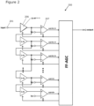
- Figure 2 shows another example embodiment of a receiver circuit 200.
- Components of Figure 2 that are also shown in Figure 1 are identified with corresponding reference numbers in the 200 series, and will not necessarily be described again here.
- the amplifiers 206 of the sub-receivers are connected to the receiver-input-terminal 201 in series with each other.
- the amplifier-input-terminal of the amplifier 206 of a first sub-receiver (which corresponds to the most significant effective threshold) is connected directly to the receiver-input-terminal 201; and the amplifier-input-terminal of each of the amplifiers 206 of the other sub-receivers is connected to the amplifier-output-terminal of the amplifier 206 of another sub-receiver.
- a series chain of sub-receivers is provided.
- the comparators 207 of the sub-receivers are configured to compare the amplifier-output-signal from its associated amplifier 206 with the same threshold value.
- the amplifiers 206 of the sub-receivers can each apply the same gain factor, such that the series connection of the amplifiers 206 results in an effective gain factor for each sub-receiver in the series to be an accumulation of the previously applied gain factors.
- the gain factor for each amplifier, after the 1 st one, in this example does not depend on the index ⁇ i> of the sub-receiver.
- Figure 2 represents another implementation for achieving the different effective threshold values that are described above.
- the sub-receivers can be provided in parallel with each other, their amplifiers can each apply the same gain factor, and the threshold values that are applied to the comparators can be different for the different sub-receivers in order to implement the different effective threshold values.
- the topology of Figure 2 is well suited for voltage signals processing, as a high bandwidth high gain amplifier can be more easily constructed from high bandwidth low gain stages.
- Figure 1 shows a purely parallel implementation of the receiver circuit
- Figure 2 shows a purely series implementation
- the receiver circuit can be implemented with a combination of parallel and series connected sub-receivers, and / or a combination of current and voltage processing modes with corresponding VI or IV conversion between them.
- the digital sub-receiver-output-signals from the sub-receivers are processed by the controller, which can be considered as applying a Feed-Forward Automatic Gain Control (FF-AGC) algorithm.
- the controller selects which sub-receiver will be used for signal processing, such that it's digital sub-receiver-output-signal is forwarded to the output.
- the controller can shutdown one or more of the sub-receivers that are not needed in order to reduce the power consumption of the receiver circuit.
- the receiver topology of Figures 1 and 2 looks and works like a flash type ADC, which estimates at calibration the strength of the input signal at the receiver-input-input.
- the sub-receivers' indexes ⁇ 0>, ⁇ 1>,... can be considered as the less significant.
- the sub-receivers' indexes ⁇ k-1>, ⁇ k-2>,... can be considered the most significant.
- Figure 3 shows schematically an example embodiment of a method of calibrating a receiver circuit, such as the ones shown in Figures 1 and 2 .
- the method of Figure 3 supposes that at initial state, all sub-receivers are active.
- the method listens for calibration-signalling such that it can detect a calibration instant.
- This can involve the method processing at least the digital sub-receiver-output-signals that corresponds to the least significant value (output ⁇ 0>), although digital sub-receiver-output-signals can be combined, in order to detect a calibration instant.
- a detectable calibration instant in signalling received at the receiver-input-terminal can be implemented in any of a number of ways, including: a long pulse (such as a pulse that is longer than a threshold duration); a start of message (SOM); and a first signal after a reset.
- the method detects ⁇ m> as the index of the most significant sub-receiver that has been triggered by the amplitude of the signal at the receiver-input-terminal. This is what is referred to above as the triggered-sub-receiver.
- the identification of the triggered-sub-receiver indicates that the signal strength has a value that is in the range between ⁇ m> (the effective threshold that is represented by the triggered-sub-receiver) and ⁇ m+1> (the effective threshold that is represented by the sub-receiver that is after the triggered-sub-receiver in the sequence).
- the output of the preceding-sub-receiver is forwarded to the receiver-output-terminal after the detected calibration instant.
- THxG ⁇ s> value should be returned to its initial value.
- the signal condition that is detected as a calibration instant can be unique and can differentiate from normal message content. Beneficially, the calibration instant can occur at the beginning of message. Less significant sub-receivers can saturate at high amplitude of input-signalling and can have a reduced reaction speed or can even get stuck at high levels. In some circumstances, a first long input signal pulse is a reasonable choice for Start-Of-Message (SOM). In this way, the receiver circuit can be calibrated at single time instant by detecting a long duration of SOM pulse.
- SOM Start-Of-Message
- examples disclosed herein are not limited to use of a long SOM pulse as a detectable calibration instant; gain calibration can be also performed in response to detecting any duration pulse, which can be outside of the message frame or can follow after a unique End-Of-Message (EOM).
- EOM End-Of-Message
- Figure 4 shows schematically another example embodiment of a method of calibrating a receiver circuit, such as the ones shown in Figures 1 and 2 .
- the sub-receiver with index ⁇ s> (which corresponds to ⁇ m-1>) remains active for input signal reception.
- the other sub-receivers are not needed to detect the change in signal amplitude and therefore they can be disabled for power saving.
- An exception to the above can be down for ⁇ s-1> sub-receiver, if its activation time can impact on performance in situation of signal strength decrease. For example, with a 2Mbaud baud rate and a signal amplitude decrease, the ⁇ s-1> sub-receiver needs to be activated in less 500ns, which can be challenging. Therefore, the implementation of the circuit can be made simpler by just keeping the ⁇ s-1> sub-receiver active.
- the example of Figure 4 can, more generally, involve the method disabling one or more of the sub-receivers, but not: i) the preceding-sub-receiver; and ii) one or more sub-receivers that are configured to apply effective threshold values that are neighbours to the effective threshold value of the preceding-sub-receiver in the sequence of weighted effective threshold values. That is, the method can:
- the method may not disable one or more sub-receivers that are configured to apply effective threshold values that have neighbouring effective threshold values that are higher than that of the preceding-sub-receiver in the sequence of weighted effective threshold values. Additionally or alternatively, the method may not disable one or more sub-receivers that are configured to apply effective threshold values that have neighbouring effective threshold values that are lower than that of the preceding-sub-receiver in the sequence of weighted effective threshold values.
- the approach described herein offers instant feedforward calibration without requiring a large circuit overhead, which can be performed by a 1st received SOM pulse of a message.
- the input dynamic range (DR) of examples disclosed herein can be reasonably large and exceed those that are known in art for AGCs, which can rarely exceed 30dB.
- Examples disclosed herein relate to a new way of Feed-Forward Automatic Gain Control, which unitizes multiple sub-receivers and re-uses them for instant high-speed feedforward gain calibration purpose.
- an auxiliary path to control the gain of the signal path, which, depending on the implementation, might require time for gain settling.
- Examples disclosed herein are well-suited to optical receiver circuits, such as those that cover a 60dB dynamic range.
- DR Dynamic Range
- IR Infra-Red
- VLC Visible-Light Communication
- ISI Inter-Symbol Interference
- the receiver's threshold should be well positioned in the middle of signal amplitude, given by its maximum and minimum amplitude envelopes.
- Two methods that can be utilized for better positioning of the effective threshold are, for example: i) use of another AGC to preserve constant signal amplitude on the comparator input; or ii) a signal amplitude peak detector can be used to adjust the effective threshold with respect to signal amplitude, as mentioned previously.
- AGC Automatic Gain Control
- High-Pass Filtering (HPF) or DC Offset Cancellation (DCOC) loops are normally utilized in the voltage domain to mitigate such and other offset sources.
- HPF High-Pass Filtering
- DCOC DC Offset Cancellation
- a half-duplex arrangement of transmitting Light Emitting Diode (LED) and receiving photodiode supposes a possibility, due to light refection in lenses or in waveguide, to have in the photodiode backward TX communication induced current, whose amplitude might exceed the amplitude of the normally received signal current.
- Receivers, utilizing HPFs or DCOCs can require a certain time to recover and should hold offsets on capacitors during the entire time of a transmitter (TX) communication.
- the hold time cannot be infinite because of charge lost due to leakages in the integrated capacitor. This creates restrictions on how long a TX communication is allowed and how fast the receiver can recover after it.
- This problem can be overcome by using a valley detector (i.e., a peak detector that is implemented such that it detects the minimum value of a signal instead of the maximum value of the signal), that does not have any recovery time after TX communication as it tracks the bottom envelope of the signal. It can mitigate against different offset sources as well as track incomplete signal return to zero level due to ISI.
- optical receiver that is described below, which can keep signal processing in the current domain, and is also able to cover the required DR and suitable for feedforward gain calibration. It can utilize current mode peak and valley signal amplitude detectors to find the position of the receiver's threshold in the middle of signal amplitude and to effectively cancel all offset source, including "dark" and ambient induced photocurrent. Due to the absence of HPFs or DCOCs, there is no recovery time after backward TX communication.
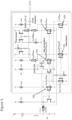
- FIG. 5 shows an optical receiver circuit.
- the optical receiver circuit is a common input circuit, presented in this embodiment by a "diode” connected n-channel MOSFET as the input of a Common Current Mirror, and multiple receiver circuits, having similar circuitry.
- the input "diode” connected n-channel MOSFET biased by IBIAS current, sets input impedance and reception bandwidth of the receiver.
- the Main Current Mirror has multiple outputs to deliver scaled signal current ISIG to multiple receiver circuits.
- sizes of output MOSFETs of the Main Current Mirror is N P-i fraction of the size of the input "diode" connected MOSFET.
- Utilization of multiple receivers enables the dynamic range (DR) of input signal ISIG to be split across multiple sub-ranges, which simplifies the requirements of the circuits, because they only need to process a limited signal sub-range. Furthermore, this approach complies with feedforward calibration, which can be performed already by amplitude of a 1 st pulse of the message.
- the illustrated implementation of a sub-receiver can be utilized in combination with different kinds of AGC as well as independent circuit solution for other applications; it is not limited to signal reception.
- Each sub-receiver utilizes outputs of the Main Current Mirror, scaled by fraction N P-i for corresponding DR sub-range, Valley and Peak Detectors, optional Current Limit and Current Comparator on the output.
- the valley detector circuit mitigates offset of the circuit itself, as well as photodiode's "dark” current IOS.
- the valley detector can be considered as a Peak Detector circuit, with a peaking peak of 2xIBIAS-ISIG-IOS-IBIAS amplitude.
- the Peak Detector peaks up the maximum of 2 currents: steady-state threshold and amplitude of ISIG/2.
- Most signal sensitive receivers may use a current limiting circuit, like the one shown in Figure 5 .
- Both Valley and Peak Detectors utilize small leakages to discharge holding capacitances, which allows the circuit to track minimum and maximum signal amplitudes and keep dynamic thresholds at the middle of the actual signal amplitude, which can vary. It can help to avoid excessive elongation or shortening of received signal pulses and associated errors at digital symbol decoding.
- a single Valley Detector can be shared between multiple receivers, especially, for ones sensing lowest signal amplitudes.
- the Valley Detector can be omitted for receivers that send the highest signal amplitudes, when offset cancellation is not needed.
- the functionality of Figure 5 can be summarised as follows.
- the receiver circuit includes the functionality of an amplifier, which comprises a current mirror (the main current mirror that is shown in Figure 5 ).
- the current mirror provides three scaled output signals: a first scaled output signal 550 that is provided to a valley detector for one or more of the plurality of sub-receivers, wherein the valley detector is configured to detect the minimum value of the first scaled output signal; a second scaled output signal 551 that is provided to a peak detector for one of the plurality of sub-receivers; and a third scaled output signal 552 for current comparison by the comparator.
- the valley detector provides two output signals: a first valley detector output signal 553, which represents the minimum value of the first scaled output signal 550, that is provided to the peak detector such that it is subtracted from the second scaled output signal 551; and a second valley detector output signal 554, which represents the minimum value of the first scaled output signal 550, for current comparison by the comparator.
- the peak detector has 2 inputs and is configured to provide on its output the highest value of these 2 inputs, either: 1st) the amplitude of the received input-signalling, minus any offset subtracted by the valley detector, divided by 2 (I SIG /2); or 2nd) the threshold value of the comparator (I TH ) - for current comparison by the comparator.
- the 1 st input of the peak detector is disabled.
- the comparator is configured to provide the digital sub-receiver-output-signal based on a comparison of the peak detector output current and a signal from the third scaled output signal 552, minus any offset subtracted by valley detector.
- each of the peak detectors and the valley detectors may comprise one or more hold capacitors, and they may be configured to discharge their holding capacitors to track amplitude / offset changes.
- Figure 6 shows another optical receiver circuit.
- the input of the Main Current Mirror "diode" connected n-channel MOSFET might be decoupled from the input terminal of the optical receiver by the input stage in the form of, for example, an open-loop common gate or by a feedback common gate stage.
- the common gate input stage sets the input impedance and reception bandwidth of the receiver, which relaxes requirements to impedance created by the "diode” connected n-channel MOSFET and reduces IBIAS current.
- an example of the common gate input stage required input impedance is created with the help of extra I IMP bias current, which is then subtracted before the input of the Main Current Mirror.
- the illustrated optical receivers which keep signal processing in the current domain, are able to cover a required dynamic range (DR) with an appropriate number of sub-receivers.
- a plurality of output MOSFETs of the Main Current Mirror can cause bandwidth limitation for a selected IBIAS current, the increase of which will deteriorate accuracy.
- number of outputs of the Main Current Mirror can be reduced with the aid of secondary Current Mirrors, for example built from p-channel MOSFETs, for a group of sub-receivers. It also enables that the counterpart of the illustrated sub-receiver circuitry can be utilized, when the input Current Mirror is built from p-channel MOSFETs.
- Figure 5 depicts an example of how to apply and subtract IBIAS in Peak, Valley Detectors and have it compensated on the input of the current comparator in the sub-receivers.
- IBIAS Peak, Valley Detectors
- an optical receiver which keeps signal processing in the current domain, is able to cover required DR, and is suitable for feedforward gain calibration. It can utilize current mode peak and valley signal amplitude detectors to find the position of receiver's threshold in the middle of signal amplitude and to effectively cancel all offset sources, including "dark" and ambient induced photocurrent. Due to the absence of HPFs or DCOCs, advantageously there is almost no recovery time after backward TX communication.
- the set of instructions/method steps described above are implemented as functional and software instructions embodied as a set of executable instructions which are effected on a computer or machine which is programmed with and controlled by said executable instructions. Such instructions are loaded for execution on a processor (such as one or more CPUs).
- processor includes microprocessors, microcontrollers, processor modules or subsystems (including one or more microprocessors or microcontrollers), or other control or computing devices.
- a processor can refer to a single component or to plural components.
- the set of instructions/methods illustrated herein and data and instructions associated therewith are stored in respective storage devices, which are implemented as one or more non-transient machine or computer-readable or computer-usable storage media or mediums.
- Such computer-readable or computer usable storage medium or media is (are) considered to be part of an article (or article of manufacture).
- An article or article of manufacture can refer to any manufactured single component or multiple components.
- the non-transient machine or computer usable media or mediums as defined herein excludes signals, but such media or mediums may be capable of receiving and processing information from signals and/or other transient mediums.
- Example embodiments of the material discussed in this specification can be implemented in whole or in part through network, computer, or data based devices and/or services. These may include cloud, internet, intranet, mobile, desktop, processor, look-up table, microcontroller, consumer equipment, infrastructure, or other enabling devices and services. As may be used herein and in the claims, the following non-exclusive definitions are provided.
- one or more instructions or steps discussed herein are automated.
- the terms automated or automatically mean controlled operation of an apparatus, system, and/or process using computers and/or mechanical/electrical devices without the necessity of human intervention, observation, effort and/or decision.
- any components said to be coupled may be coupled or connected either directly or indirectly.
- additional components may be located between the two components that are said to be coupled.
Landscapes
- Engineering & Computer Science (AREA)
- Computer Networks & Wireless Communication (AREA)
- Signal Processing (AREA)
- Power Engineering (AREA)
- Physics & Mathematics (AREA)
- Electromagnetism (AREA)
- Circuits Of Receivers In General (AREA)
- Control Of Amplification And Gain Control (AREA)
Priority Applications (3)
| Application Number | Priority Date | Filing Date | Title |
|---|---|---|---|
| EP23168998.5A EP4451561A1 (de) | 2023-04-20 | 2023-04-20 | Empfängerschaltung |
| CN202410306185.2A CN118826766A (zh) | 2023-04-20 | 2024-03-18 | 接收器电路 |
| US18/632,373 US12494807B2 (en) | 2023-04-20 | 2024-04-11 | Receiver circuit |
Applications Claiming Priority (1)
| Application Number | Priority Date | Filing Date | Title |
|---|---|---|---|
| EP23168998.5A EP4451561A1 (de) | 2023-04-20 | 2023-04-20 | Empfängerschaltung |
Publications (1)
| Publication Number | Publication Date |
|---|---|
| EP4451561A1 true EP4451561A1 (de) | 2024-10-23 |
Family
ID=86096008
Family Applications (1)
| Application Number | Title | Priority Date | Filing Date |
|---|---|---|---|
| EP23168998.5A Pending EP4451561A1 (de) | 2023-04-20 | 2023-04-20 | Empfängerschaltung |
Country Status (3)
| Country | Link |
|---|---|
| US (1) | US12494807B2 (de) |
| EP (1) | EP4451561A1 (de) |
| CN (1) | CN118826766A (de) |
Citations (3)
| Publication number | Priority date | Publication date | Assignee | Title |
|---|---|---|---|---|
| US20040145402A1 (en) * | 2000-07-03 | 2004-07-29 | Burns Lawrence M. | Extended range variable-gain amplifier |
| US20070286609A1 (en) * | 2006-01-13 | 2007-12-13 | Quazi Ikram | Bias circuit for Burst-Mode/TDM systems with power save feature |
| US20140376666A1 (en) * | 2012-03-06 | 2014-12-25 | Fraunhofer-Gesellschaft Zur Foerderung Der Angewandten Forschung E.V. | Receiving stage and method for receiving |
Family Cites Families (19)
| Publication number | Priority date | Publication date | Assignee | Title |
|---|---|---|---|---|
| GB2280998A (en) | 1993-08-11 | 1995-02-15 | Plessey Semiconductors Ltd | Fast-acting feed-forward automatic gain-control arrangement |
| GB2307806A (en) | 1995-11-28 | 1997-06-04 | Plessey Semiconductors Ltd | Automatic gain control using a cascade of amplifiers and feed-forward |
| US6304357B1 (en) | 1997-03-13 | 2001-10-16 | Hitachi, Ltd. | Optical receiver |
| KR100605777B1 (ko) | 2002-04-25 | 2006-07-31 | 삼성전자주식회사 | 버스트모드 광 수신기의 판별 임계값 제어장치 |
| KR100537902B1 (ko) | 2003-03-29 | 2005-12-20 | 한국전자통신연구원 | 버스트 모드 광 수신 장치 |
| JP4568205B2 (ja) | 2005-10-14 | 2010-10-27 | 株式会社東芝 | 受信装置 |
| US7265626B2 (en) * | 2005-12-20 | 2007-09-04 | Avago Technologies Ecbu Ip (Singapore) Pte. Ltd. | Fast-setting digital automatic gain control |
| JP5270071B2 (ja) | 2006-05-16 | 2013-08-21 | 富士通オプティカルコンポーネンツ株式会社 | 信号増幅装置 |
| KR100866091B1 (ko) | 2007-02-28 | 2008-10-31 | 고려대학교 산학협력단 | 문턱 전압을 수렴시키는 광수신 장치, 이를 이용하는광수신 오디오 장치 및 광통신 장치 |
| TW200932194A (en) | 2008-01-29 | 2009-08-01 | Univ Nat Taiwan | A feed-forward automatic-gain control amplifier (FFAGCA) for biomedical application |
| US7835098B2 (en) | 2008-05-28 | 2010-11-16 | Texas Instruments Incorporated | Automatic gain control for magnetic disk-drive preamplifier |
| EP2391003A1 (de) | 2010-05-24 | 2011-11-30 | University College Cork | Linearer Burstmodusempfänger |
| US8705985B2 (en) | 2010-06-02 | 2014-04-22 | Mellanox Technologies Denmark Aps | Fast optical receiver for unencoded data |
| US9252889B2 (en) | 2011-11-03 | 2016-02-02 | Mellanox Technologies Denmark Aps | Fast optical receiver |
| WO2017023240A1 (en) | 2015-07-31 | 2017-02-09 | Hewlett Packard Enterprise Development Lp | Optical receivers |
| US10171057B1 (en) | 2018-03-21 | 2019-01-01 | Elenion Technologies, Llc | Automatic gain control loop |
| US11005573B2 (en) | 2018-11-20 | 2021-05-11 | Macom Technology Solutions Holdings, Inc. | Optic signal receiver with dynamic control |
| CN111130477B (zh) | 2019-12-06 | 2023-04-25 | 上海交通大学 | 电平触发型的自动调节增益放大电路 |
| CN114900143B (zh) | 2022-07-11 | 2022-11-08 | 南京燧锐科技有限公司 | 自动增益控制电路及其控制方法 |
-
2023
- 2023-04-20 EP EP23168998.5A patent/EP4451561A1/de active Pending
-
2024
- 2024-03-18 CN CN202410306185.2A patent/CN118826766A/zh active Pending
- 2024-04-11 US US18/632,373 patent/US12494807B2/en active Active
Patent Citations (3)
| Publication number | Priority date | Publication date | Assignee | Title |
|---|---|---|---|---|
| US20040145402A1 (en) * | 2000-07-03 | 2004-07-29 | Burns Lawrence M. | Extended range variable-gain amplifier |
| US20070286609A1 (en) * | 2006-01-13 | 2007-12-13 | Quazi Ikram | Bias circuit for Burst-Mode/TDM systems with power save feature |
| US20140376666A1 (en) * | 2012-03-06 | 2014-12-25 | Fraunhofer-Gesellschaft Zur Foerderung Der Angewandten Forschung E.V. | Receiving stage and method for receiving |
Also Published As
| Publication number | Publication date |
|---|---|
| US20240356572A1 (en) | 2024-10-24 |
| CN118826766A (zh) | 2024-10-22 |
| US12494807B2 (en) | 2025-12-09 |
Similar Documents
| Publication | Publication Date | Title |
|---|---|---|
| US10305605B2 (en) | Optical receiver, optical transceiver comprising the same, and method of protecting a photodetector in the optical receiver with a transient event or a transient state determination | |
| US10003410B2 (en) | Optical receiver, optical termination device, and optical communication system | |
| US9853618B2 (en) | Transimpedance amplifier circuit | |
| EP1357717B1 (de) | Vorrichtung zur automatischen Anpassung der Entscheidungsschwelle in einem optischen Empfänger für Burstbetrieb | |
| JP4532563B2 (ja) | 光受信器およびその識別閾値生成方法 | |
| US8948610B2 (en) | Data signal threshold detection and/or recovery in optical and/or optoelectric receivers and/or transceivers | |
| US20150270808A1 (en) | Transimpedance amplifier | |
| JPH10303992A (ja) | 識別レベル制御回路 | |
| EP1355464A2 (de) | Gleichspannungsbeseitigung in einem optischen Empfänger | |
| CN103262444A (zh) | 主站侧装置 | |
| US9325426B2 (en) | Burst-mode receiver having a wide dynamic range and low pulse-width distortion and a method | |
| US20200322063A1 (en) | Signal detection circuit, optical receiver, master station device, and signal detection method | |
| JP6661057B1 (ja) | リミッティング増幅回路 | |
| US12494807B2 (en) | Receiver circuit | |
| CN100463362C (zh) | 接收方法以及接收电路 | |
| JP2962218B2 (ja) | ディジタル光受信回路 | |
| EP3651358B1 (de) | Automatische verstärkungsregelung für passives optisches netzwerk | |
| JP4760312B2 (ja) | 光受信器 | |
| US9621972B2 (en) | Burst-mode receiver | |
| JP3484055B2 (ja) | 光受信回路 | |
| JP2000201113A (ja) | バ―スト光信号の受信方法及びその装置 | |
| US7689122B2 (en) | Polarity-insensitive signal detect circuit for use with any signal sequence | |
| KR101043954B1 (ko) | 감쇄기를 이용한 광수신기의 임계값 판별장치 | |
| TWI890444B (zh) | 光通訊耦合模塊及其操作方法 | |
| JP2001211040A (ja) | デジタル信号増幅回路及び光受信回路 |
Legal Events
| Date | Code | Title | Description |
|---|---|---|---|
| PUAI | Public reference made under article 153(3) epc to a published international application that has entered the european phase |
Free format text: ORIGINAL CODE: 0009012 |
|
| STAA | Information on the status of an ep patent application or granted ep patent |
Free format text: STATUS: THE APPLICATION HAS BEEN PUBLISHED |
|
| AK | Designated contracting states |
Kind code of ref document: A1 Designated state(s): AL AT BE BG CH CY CZ DE DK EE ES FI FR GB GR HR HU IE IS IT LI LT LU LV MC ME MK MT NL NO PL PT RO RS SE SI SK SM TR |
|
| STAA | Information on the status of an ep patent application or granted ep patent |
Free format text: STATUS: REQUEST FOR EXAMINATION WAS MADE |
|
| 17P | Request for examination filed |
Effective date: 20250423 |