EP4456331A1 - Antennenmodul und herstellungsverfahren dafür - Google Patents
Antennenmodul und herstellungsverfahren dafür Download PDFInfo
- Publication number
- EP4456331A1 EP4456331A1 EP22910555.6A EP22910555A EP4456331A1 EP 4456331 A1 EP4456331 A1 EP 4456331A1 EP 22910555 A EP22910555 A EP 22910555A EP 4456331 A1 EP4456331 A1 EP 4456331A1
- Authority
- EP
- European Patent Office
- Prior art keywords
- substrate
- layer
- gallium nitride
- element portion
- graphene layer
- Prior art date
- Legal status (The legal status is an assumption and is not a legal conclusion. Google has not performed a legal analysis and makes no representation as to the accuracy of the status listed.)
- Pending
Links
Images



Classifications
-
- C—CHEMISTRY; METALLURGY
- C01—INORGANIC CHEMISTRY
- C01B—NON-METALLIC ELEMENTS; COMPOUNDS THEREOF; METALLOIDS OR COMPOUNDS THEREOF NOT COVERED BY SUBCLASS C01C
- C01B32/00—Carbon; Compounds thereof
- C01B32/15—Nano-sized carbon materials
- C01B32/182—Graphene
- C01B32/184—Preparation
- C01B32/188—Preparation by epitaxial growth
-
- C—CHEMISTRY; METALLURGY
- C01—INORGANIC CHEMISTRY
- C01B—NON-METALLIC ELEMENTS; COMPOUNDS THEREOF; METALLOIDS OR COMPOUNDS THEREOF NOT COVERED BY SUBCLASS C01C
- C01B32/00—Carbon; Compounds thereof
- C01B32/15—Nano-sized carbon materials
- C01B32/182—Graphene
- C01B32/184—Preparation
-
- H—ELECTRICITY
- H01—ELECTRIC ELEMENTS
- H01P—WAVEGUIDES; RESONATORS, LINES, OR OTHER DEVICES OF THE WAVEGUIDE TYPE
- H01P11/00—Apparatus or processes specially adapted for manufacturing waveguides or resonators, lines, or other devices of the waveguide type
-
- H—ELECTRICITY
- H01—ELECTRIC ELEMENTS
- H01Q—ANTENNAS, i.e. RADIO AERIALS
- H01Q1/00—Details of, or arrangements associated with, antennas
- H01Q1/12—Supports; Mounting means
- H01Q1/22—Supports; Mounting means by structural association with other equipment or articles
- H01Q1/2283—Supports; Mounting means by structural association with other equipment or articles mounted in or on the surface of a semiconductor substrate as a chip-type antenna or integrated with other components into an IC package
-
- H—ELECTRICITY
- H01—ELECTRIC ELEMENTS
- H01Q—ANTENNAS, i.e. RADIO AERIALS
- H01Q1/00—Details of, or arrangements associated with, antennas
- H01Q1/36—Structural form of radiating elements, e.g. cone, spiral, umbrella; Particular materials used therewith
- H01Q1/364—Structural form of radiating elements, e.g. cone, spiral, umbrella; Particular materials used therewith using a particular conducting material, e.g. superconductor
- H01Q1/368—Structural form of radiating elements, e.g. cone, spiral, umbrella; Particular materials used therewith using a particular conducting material, e.g. superconductor using carbon or carbon composite
-
- H—ELECTRICITY
- H01—ELECTRIC ELEMENTS
- H01Q—ANTENNAS, i.e. RADIO AERIALS
- H01Q1/00—Details of, or arrangements associated with, antennas
- H01Q1/36—Structural form of radiating elements, e.g. cone, spiral, umbrella; Particular materials used therewith
- H01Q1/38—Structural form of radiating elements, e.g. cone, spiral, umbrella; Particular materials used therewith formed by a conductive layer on an insulating support
-
- H—ELECTRICITY
- H01—ELECTRIC ELEMENTS
- H01Q—ANTENNAS, i.e. RADIO AERIALS
- H01Q23/00—Antennas with active circuits or circuit elements integrated within them or attached to them
-
- H—ELECTRICITY
- H10—SEMICONDUCTOR DEVICES; ELECTRIC SOLID-STATE DEVICES NOT OTHERWISE PROVIDED FOR
- H10D—INORGANIC ELECTRIC SEMICONDUCTOR DEVICES
- H10D30/00—Field-effect transistors [FET]
- H10D30/01—Manufacture or treatment
- H10D30/015—Manufacture or treatment of FETs having heterojunction interface channels or heterojunction gate electrodes, e.g. HEMT
-
- H—ELECTRICITY
- H10—SEMICONDUCTOR DEVICES; ELECTRIC SOLID-STATE DEVICES NOT OTHERWISE PROVIDED FOR
- H10D—INORGANIC ELECTRIC SEMICONDUCTOR DEVICES
- H10D30/00—Field-effect transistors [FET]
- H10D30/01—Manufacture or treatment
- H10D30/061—Manufacture or treatment of FETs having Schottky gates
-
- H—ELECTRICITY
- H10—SEMICONDUCTOR DEVICES; ELECTRIC SOLID-STATE DEVICES NOT OTHERWISE PROVIDED FOR
- H10D—INORGANIC ELECTRIC SEMICONDUCTOR DEVICES
- H10D30/00—Field-effect transistors [FET]
- H10D30/40—FETs having zero-dimensional [0D], one-dimensional [1D] or two-dimensional [2D] charge carrier gas channels
- H10D30/47—FETs having zero-dimensional [0D], one-dimensional [1D] or two-dimensional [2D] charge carrier gas channels having two-dimensional [2D] charge carrier gas channels, e.g. nanoribbon FETs or high electron mobility transistors [HEMT]
-
- H—ELECTRICITY
- H10—SEMICONDUCTOR DEVICES; ELECTRIC SOLID-STATE DEVICES NOT OTHERWISE PROVIDED FOR
- H10D—INORGANIC ELECTRIC SEMICONDUCTOR DEVICES
- H10D30/00—Field-effect transistors [FET]
- H10D30/40—FETs having zero-dimensional [0D], one-dimensional [1D] or two-dimensional [2D] charge carrier gas channels
- H10D30/47—FETs having zero-dimensional [0D], one-dimensional [1D] or two-dimensional [2D] charge carrier gas channels having two-dimensional [2D] charge carrier gas channels, e.g. nanoribbon FETs or high electron mobility transistors [HEMT]
- H10D30/471—High electron mobility transistors [HEMT] or high hole mobility transistors [HHMT]
- H10D30/475—High electron mobility transistors [HEMT] or high hole mobility transistors [HHMT] having wider bandgap layer formed on top of lower bandgap active layer, e.g. undoped barrier HEMTs such as i-AlGaN/GaN HEMTs
-
- H—ELECTRICITY
- H10—SEMICONDUCTOR DEVICES; ELECTRIC SOLID-STATE DEVICES NOT OTHERWISE PROVIDED FOR
- H10D—INORGANIC ELECTRIC SEMICONDUCTOR DEVICES
- H10D30/00—Field-effect transistors [FET]
- H10D30/80—FETs having rectifying junction gate electrodes
- H10D30/87—FETs having Schottky gate electrodes, e.g. metal-semiconductor FETs [MESFET]
-
- H—ELECTRICITY
- H10—SEMICONDUCTOR DEVICES; ELECTRIC SOLID-STATE DEVICES NOT OTHERWISE PROVIDED FOR
- H10D—INORGANIC ELECTRIC SEMICONDUCTOR DEVICES
- H10D62/00—Semiconductor bodies, or regions thereof, of devices having potential barriers
- H10D62/80—Semiconductor bodies, or regions thereof, of devices having potential barriers characterised by the materials
- H10D62/85—Semiconductor bodies, or regions thereof, of devices having potential barriers characterised by the materials being Group III-V materials, e.g. GaAs
- H10D62/8503—Nitride Group III-V materials, e.g. AlN or GaN
Definitions
- the present invention relates to an antenna module using graphene as antenna elements and/or wiring and integrally formed with active elements such as amplifiers.
- a graphene film formed by the CVD method on a copper foil is transferred to a substrate, an Au film is provided on the transferred graphene film as appropriate, and the antenna element is formed by patterning with photolithography, etching, UV-ozone treatment, etc. In this way, an antenna element of the desired shape can be fabricated on the substrate.
- Patent Document 1 JP2019-75626A
- the antenna used in mobile communication systems by the way, is used together with an amplifier that amplifies the signal transmitted or received by the antenna element.
- the transmission distance between the amplifier and the antenna element should be extremely short (e.g., less than 100 ⁇ m).
- Patent Document 1 only shows the feasibility of the antenna element as a stand-alone device, and there is no specific teaching on its application to a device combined with the amplifier and other devices.
- the present invention was made in view of the above and is intended to provide an antenna module suitable for use in signal frequency bands from several 10 GHz to 100 GHz and above.
- An antenna module comprises a substrate with at least the top surface being a single crystal of silicon carbide; a single-crystal graphene layer provided in contact with the top surface of the substrate; and a gallium nitride layer on the substrate.
- the antenna module is characterized in that an antenna element portion is formed by patterning a region in the graphene layer that is not covered by the gallium nitride layer, an active element portion is formed in the gallium nitride layer, and a connection portion connecting the antenna element portion and the active element portion are integrally formed.
- the gallium nitride layer may be provided to cover a part of the graphene layer.
- the substrate may be a hybrid substrate with a single crystal layer of silicon carbide fabricated on an insulator base substrate.
- the gallium nitride layer may be a layer epitaxially grown on the graphene layer as a buffer layer.
- the active element portion may include an amplifier using a HEMT (High Electron Mobility Transistor) formed in the gallium nitride layer.
- HEMT High Electron Mobility Transistor
- connection portion may connect the antenna element portion and the active element portion with a length of less than 100 ⁇ m.
- the method of manufacturing an antenna module comprises: a step of preparing a substrate of which at least the top surface is a single crystal of silicon carbide; a step of forming a graphene layer on the top surface of the substrate; a step of epitaxially growing a gallium nitride layer using the graphene layer as a buffer layer; a step of forming an active element portion including an amplifier in the gallium nitride layer; a step of exposing the graphene layer by removing the area of the gallium nitride layer in which the active element portion is not provided; and a step of forming an antenna element and a connection portion connecting the active element portion with the antenna element by patterning the exposed graphene layer.
- the method of manufacturing an antenna module comprises: a step of preparing a substrate of which at least the top surface is a single crystal of silicon carbide; a step of forming a graphene layer on the top surface of the substrate; a step of removing a portion of the graphene layer and forming an antenna element and a connection portion connecting the active element portion with the antenna element by patterning the graphene layer; a step of epitaxially growing a gallium nitride layer in the area where the graphene layer has been removed; and a step of forming an active element portion including an amplifier in the gallium nitride layer;
- the method of manufacturing an antenna module comprises: a step of preparing a substrate of which at least the top surface is a single crystal of silicon carbide; a step of forming a graphene layer on the top surface of the substrate; a step of forming an antenna element by patterning the graphene layer; and a step of providing a gallium nitride layer by bonding a gallium nitride device with an active element portion including an amplifier to the graphene layer on the substrate.
- an electrode pad and a connection portion connecting the antenna element to the electrode pad may be formed together with the antenna element, and in the step of providing the gallium nitride layer, the gallium nitride device may be bonded to the graphene layer on the substrate so that an electrode on the gallium nitride device and the electrode pad are electrically connected.
- the graphene layer may be epitaxially grown by sublimating the silicon atoms in a single crystal of silicon carbide on the top surface of the substrate.
- the substrate may be a hybrid substrate with a single-crystal layer of silicon carbide fabricated on an insulator base substrate.
- an antenna element using graphene and an active element such as an amplifier are formed integrally, making it possible to realize an antenna module suitable for use in the signal frequency band from several 10 GHz to 100 GHz or higher.
- Fig. 1 is a schematic diagram of the structure of an antenna module 1 according to the embodiment of the present invention.
- the antenna module 1 has a layer structure consisting of a substrate 2, a graphene layer 3, and a gallium nitride (GaN) layer 4 stacked in this order.
- the antenna module 1 then utilizes the aforementioned layer structure to realize an antenna element portion 10, an active element portion 12, and a connection portion 14, as shown in Fig. 1 .
- the substrate 2 is the basis for forming the graphene layer 3.
- the top surface 21 in contact with the graphene layer 3 is a single-crystal silicon carbide (SiC).
- the rest of the substrate 2, except the top surface, may be an insulator different from SiC. That is, the substrate 2 may be a single-crystal substrate of SiC or a hybrid substrate with a single-crystal layer of SiC fabricated on an insulator.
- the surface of the single-crystal layer of SiC in the substrate 2 may be (0001) surface.
- the substrate 2 is the basis for epitaxial growth of graphene that forms the graphene layer 3.
- the graphene layer 3 is provided in contact with the top surface of the substrate 2.
- the graphene layer 3 is composed of a single layer or multiple layers of single-crystal graphene.
- the graphene layer 3 functions as a buffer layer between the substrate 2 and the GaN layer 4.
- the graphene layer 3 constitutes the antenna element portion 10 and the connection portion 14 by patterning into the desired antenna shape.
- the GaN layer 4 is provided on top of the substrate 2.
- the GaN layer 4 is overlaid on the graphene layer 3, as shown in Fig. 1(a) .
- the GaN layer 4 may be provided directly on the substrate 2 without the graphene layer 3, as shown in Fig. 1(b) .
- amplifiers and other devices that constitute the active element portion 12 are formed using devices capable of high-speed operation, such as HEMTs (High Electron Mobility Transistors).
- a metal film e.g., Au film
- a protective film e.g., Au film
- the antenna element portion 10 In the antenna module 1 with a layer configuration of the substrate 2, the graphene layer 3, and the GaN layer 4, the antenna element portion 10, the active element portion 12, and the connection portion 14 are provided by partitioning regions in the plane of the substrate 2. As shown in Fig. 1 , the active element portion 12 is provided in the GaN layer 4.
- the active element portion 12 may include other active elements in addition to the amplifiers described above.
- the active element portion 12 may include electrodes 42 to which wiring from the outside (e.g., antenna element portion 10 or connection portion 14) is connected.
- the electrode 42 may be provided on the surface of the GaN layer 4 facing the substrate 2 or on the surface opposite to the surface facing the substrate 2.
- the GaN layer 4 is not provided in the antenna element portion 10.
- the antenna element portion 10 has a structure in which the graphene layer 3 is patterned into a shape to achieve the desired antenna properties.
- a metal film such as Au may be overlaid on some or all of the patterned graphene.
- Graphene has higher values of various properties such as electrical conductivity, carrier mobility, and thermal conductivity than copper (Cu) and other metals and ITO, so it is possible to achieve antenna properties superior to those of Cu and to suppress property degradation even when antenna size is reduced.
- connection portion 14 is the wiring that connects the electrode 42 of the amplifier of the active element portion 12 to the antenna element portion 10.
- the connection portion 14 may not be provided with the GaN layer 4, or the connection portion 14 may have a GaN layer 4 overlaid on part or all of the connection portion 14.
- the connection portion 14 may be formed by patterning the graphene layer 3 or by a metal film such as Au.
- the connection portion 14 may be formed partly by a metal film and partly by graphene in other parts, or there may be parts where the metal film is overlaid on the graphene. If the antenna element portion 10 and the connection portion 14 are formed solely of graphene, transparent wiring can be achieved.
- connection portion 14 should be formed as short as possible (e.g., so that the transmission distance is preferably less than 100 ⁇ m, more preferably less than 30 ⁇ m, and even more preferably less than 10 um) so that the signal transmitted between the active element portion 12 and the antenna element portion 10 is not degraded.
- the electrode 42 and the electrode pad 15 provided at one end of the connection 14 may be connected directly or indirectly with a conductor between them, as shown in Fig. 2(a) .
- the electrode 42 When the electrode 42 is provided on the opposite surface of the GaN layer 4 from the surface facing the substrate 2, the electrode 42 may be connected to the connection portion 14a by wire bonding 14a, as shown in Fig. 2(b) .
- a conductor layer 14b such as metal, graphene, etc., may be added to connect the electrode 42 to the connection portion 14.
- the manufacturing method of the antenna module 1 is then described.
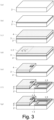
- Fig. 3 shows the first example of the procedure for fabricating the antenna module.
- the substrate 2 is prepared( Figure 3(a) ).
- At least the top surface in the substrate 2 is a single-crystal SiC, as described above.
- the crystal structure of this top surface SiC is preferably of 4H-SiC, 6H-SiC, or 3C-SiC.
- any of single-crystal silicon, sapphire, polycrystalline silicon, alumina, silicon nitride, aluminum nitride, diamond, or polycrystalline SiC is used as the base substrate, and a film of silicon oxide, single-crystal silicon, polycrystalline silicon, amorphous silicon, alumina, silicon nitride, silicon carbide, aluminum nitride, or diamond is provided on the base substrate as necessary, and the base substrate and silicon carbide substrate are bonded by performing a surface treatment on the bonding surfaces of the base substrate and silicon carbide substrate.
- a hybrid substrate with a single-crystal layer of SiC thinned by grinding and polishing, ion implantation stripping method etc. can be fabricated.
- the ion implantation stripping method hydrogen or helium ions are implanted into the silicon carbide substrate before peeling, and after bonding, the substrate is peeled off at the ionimplantation interface by heat treatment.
- CVD is performed on the surface with polycrystalline SiC, and then the base substrate may be removed to obtain the hybrid substrate with the single-crystal layer of SiC on the insulator.
- the substrate 2 is preferably heated to 1,100°C or higher to sublimate silicon atoms (Si) near the top surface of the substrate 2 to form a graphene film of the desired thickness (e.g., 50 to 1,500 nm) to form graphene layer 3 ( Fig. 3(b) ).
- Si silicon atoms
- An example of typical growth conditions for graphene is heating for 5 to 30 minutes in an argon (Ar) atmosphere at an atmospheric pressure of 10 5 Pa (1 bar) and a temperature of 1500 to 1600°C.
- Ar argon
- a nanocarbon film of either fullerene, graphene, or carbon nanotube is formed, but the preparation conditions should be adjusted appropriately to obtain graphene.
- the graphene layer 3 formed in this way grows so-called epitaxially so that the crystal is oriented in a predetermined direction relative to the crystal plane of the top SiC single crystal of the base substrate 2.
- GaN gallium nitride
- MOCVD metal organic chemical vapor deposition
- TMGa trimethylgallium
- TMAl trimethylaluminum
- NH 3 ammonia
- the substrate 2 with graphene layer 3 may be thermally cleaned at 1100°C for about 5 minutes in an H 2 atmosphere.
- An AlN buffer layer of several 10 to several 100 nm may be grown on the substrate surface after cleaning, followed by the growth of an undoped GaN layer 4 about 2 um thick at 1050°C.
- the AlN buffer layer may be grown so that a high-temperature AlN buffer layer grown at about 1080°C is stacked on top of a low-temperature AlN buffer layer grown at about 780°C.
- the graphene layer 3 is used as a nucleation layer (template layer) for GaN epi-crystals.
- the graphene layer 3 may be removed for the area where GaN is to be grown (that is, the area where the active element portion is to be provided) so that GaN is directly grown on the SiC single crystal of the top surface 21 of substrate 2.
- active elements such as HEMTs, passive elements such as resistors, capacitors, inductors, wiring, and electrodes 42, etc. are formed in the grown GaN layer 4 to form active element portion 12 including amplifiers, etc. ( Fig. 3(d) ).
- the GaN layer 4 is removed from the areas other than the active element portion 12 by etching to expose the graphene layer 3 ( Fig. 3(e) ).
- the antenna element portion 10 and the connection portion 14 are patterned on the graphene layer 3 ( Fig. 3(f) ). This patterning can be performed, for example, by depositing an Au film on the graphene layer 3, patterning the Au film using photolithography and etching techniques, removing the exposed graphene not covered by the Au film by UV-ozone treatment, etc., and then removing the unnecessary parts of the Au film.
- connection portion 14 electrically connect the electrode 42 of the active element portion 12 to the connection portion 14 ( Fig. 3(g) ).
- the electrode 42 may be connected to the connection portion 14 by wire bonding ( Fig. 2(b) ) or by adding graphene or a thin metal film ( Fig. 2(c) ).
- a monolithic antenna module can be fabricated in which the antenna element portion 10 and the active element portion 12 are provided on the substrate 2, and the two are connected by the connection portion 14.
- the formation of the active element part 12 and the formation of the antenna element part 10 and the connection part 14 may be performed in different orders, or some or all of the processes may be performed simultaneously.
- the antenna module 1 fabricated as described above has the antenna element portion 10 and the active element portion 12 in close proximity, and the two are connected by a very short connection portion 14, thereby suppressing degradation of the signal propagating between the antenna element portion 10 and the active element portion 12 even in the signal frequency band from several 10 GHz to 100 GHz or higher.
- the graphene layer 3 is a single-crystal film formed by epitaxial growth on the SiC single-crystal on the top surface of the substrate. This results in superior graphene properties (conductivity, carrier mobility, thermal conductivity, film strength, etc.) compared to the method of transferring a separately fabricated polycrystalline graphene film onto the substrate.
- Antenna elements made by patterning such single-crystal graphene are expected to have superior characteristics compared to antenna elements made of polycrystalline graphene as well as antenna elements made of thin metal films such as copper, and the characteristics will not deteriorate even if the antenna size is reduced.
- both the graphene layer 3 and the GaN layer 4 are formed so that the crystals are oriented in respective predetermined directions relative to the crystal plane of the single-crystal SiC on the top surface of the substrate 2.
- the graphene layer 3 and the GaN layer 4 are oriented so that their crystals form a relatively predetermined angle. This can suppress the electrical resistance and parasitic resistance between the GaN-HEMT and the graphene antenna, thereby improving the antenna's radiation efficiency and other characteristics.
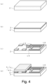
- Fig. 4 shows the second example of the procedure for fabricating an antenna module. This procedure differs from the first example described above in that the GaN layer is provided by separately preparing a GaN device 41 without epitaxial growth of the GaN layer 4 and bonding the GaN device 41 to the substrate 2 on which the graphene layer 3 is provided.
- a substrate 2 is prepared ( Fig. 4(a) ) and a graphene layer 3 is formed on the top surface of the substrate 2 ( Fig. 4(b) ) using the same method described with reference to Figs. 3(a) and (b) .
- the antenna element portion 10 and the connection portion 14 are patterned on the graphene layer 3 ( Fig. 4(c) ).
- Other patterns of graphene layer 3 (or Au film on top of it) required for bonding with GaN device 41 may also be formed.
- the graphene layer 3 may function as an adhesive layer to bond the active element portion 12 to the substrate 2.
- the patterning can be done, for example, by depositing an Au film on the graphene layer 3, patterning the Au film using photolithography and etching techniques, removing the exposed graphene not covered by the Au film by UV-ozone treatment, etc., and then removing the unnecessary parts of the Au film In this way, the antenna element portion 10 can be formed monolithically on the substrate 2.
- the pattern used for bonding with the GaN device 41 may be formed by removing the graphene layer 3 and using only a thin metal film such as Au.
- the pattern used for bonding to the GaN device 41 may be made of graphene, thin metal films, or stacks of these.
- the pattern used for bonding to the GaN device 41 may also serve the function of ensuring an electrical connection between the elements in the GaN device 41 and the outside, as well as the electrode pad 15 connected to the electrode 42.
- the GaN device 41 is a GaN substrate on which the amplifiers and other elements that constitute the active element portion 12 are formed and cut into predetermined dimensions.
- the surface of the GaN device 41 (the surface that is bonded to the substrate 2) is provided with electrodes 42 for exchanging signals with the elements in the active element portion 12.
- the electrode 42 of the GaN device 41 is electrically connected to the electrode pad 15 on the substrate 2.
- the bonding of the GaN device 41 and the substrate 2 may be performed after activation or surface treatment is performed on the surfaces of both.
- the GaN device 41 can also be bonded to the substrate 2 by flip chip bonding.
- the GaN device 41 bonded to the substrate 2 serves as the GaN layer 4 in the antenna module 1.
- an integrated antenna module can be fabricated in which the antenna element portion 10 and the active element portion 12 are provided on the substrate 2, and the two are connected by the connection portion 14.
- the antenna module 1 fabricated as described above has the antenna element portion 10 and the active element portion 12 in close proximity, and the two are connected by a very short connection portion 14, thereby suppressing degradation of the signal propagating between the antenna element portion 10 and the active element portion 12 even in the signal frequency band from several 10 GHz to 100 GHz or higher.
- the graphene layer 3 is a single-crystal film formed by epitaxial growth on the single-crystal SiC on the top surface of the substrate. This results in superior graphene properties (conductivity, carrier mobility, thermal conductivity, film strength, etc.) compared to the method of transferring a separately fabricated polycrystalline graphene film onto the substrate.
- Antenna elements made by patterning such single-crystal graphene are expected to have superior characteristics compared to antenna elements made of polycrystalline graphene as well as antenna elements made of thin metal films such as copper, and the characteristics will not deteriorate even if the antenna size is reduced.
- the GaN device 41 with the active element portion 12 can be separately prepared and then bonded to the substrate 2, which provides a high degree of freedom in the design of the active element portion 12.
- the antenna module 1 can be made in various variations while keeping the antenna element portion 10 in common.
- the present invention is not limited to the above embodiments or examples.
- the antenna element portion 10 and the active element portion 12 are provided on the same side of the substrate 2.
- the antenna element portion 10 may be provided on the opposite side of the substrate 2 from the side where the active element portion 12 is provided.
- the connection portion 14 connecting the antenna element portion 10 and the active element portion 12 may include a through-substrate via 14c that passes through the substrate 2 and electrically connects both sides of the substrate.
- the graphene layer 3 may be provided on both sides of the substrate 2, and the wiring of the connection portion 14 drawn to the active element portion 12, the electrode pad to be bonded to the active element portion 12, and the antenna element portion 10 may be made of graphene.
- the electrode 42 was provided on the substrate bonding surface of the active element portion 12, and electrode pad 15 on substrate 2 was directly connected to electrode 42, but electrode 42 may be provided on the opposite side of the GaN layer 4 from the side facing substrate 2. In this case, the electrode pad 15 may not be provided on the substrate, and the electrode 42 may be connected to the connection portion 14 by wire bonding or adding a conductor layer, as shown in Fig. 2(b) .
Landscapes
- Chemical & Material Sciences (AREA)
- Engineering & Computer Science (AREA)
- Organic Chemistry (AREA)
- Microelectronics & Electronic Packaging (AREA)
- Materials Engineering (AREA)
- Nanotechnology (AREA)
- Inorganic Chemistry (AREA)
- Manufacturing & Machinery (AREA)
- Composite Materials (AREA)
- Junction Field-Effect Transistors (AREA)
- Details Of Aerials (AREA)
- Carbon And Carbon Compounds (AREA)
- Variable-Direction Aerials And Aerial Arrays (AREA)
- Semiconductor Integrated Circuits (AREA)
Applications Claiming Priority (2)
| Application Number | Priority Date | Filing Date | Title |
|---|---|---|---|
| JP2021207486A JP7765040B2 (ja) | 2021-12-21 | 2021-12-21 | アンテナモジュールおよびその製造方法 |
| PCT/JP2022/039252 WO2023119833A1 (ja) | 2021-12-21 | 2022-10-21 | アンテナモジュールおよびその製造方法 |
Publications (2)
| Publication Number | Publication Date |
|---|---|
| EP4456331A1 true EP4456331A1 (de) | 2024-10-30 |
| EP4456331A4 EP4456331A4 (de) | 2025-12-10 |
Family
ID=86901997
Family Applications (1)
| Application Number | Title | Priority Date | Filing Date |
|---|---|---|---|
| EP22910555.6A Pending EP4456331A4 (de) | 2021-12-21 | 2022-10-21 | Antennenmodul und herstellungsverfahren dafür |
Country Status (7)
| Country | Link |
|---|---|
| US (1) | US20240339747A1 (de) |
| EP (1) | EP4456331A4 (de) |
| JP (1) | JP7765040B2 (de) |
| KR (1) | KR20240127343A (de) |
| CN (1) | CN118541876A (de) |
| TW (1) | TW202327163A (de) |
| WO (1) | WO2023119833A1 (de) |
Families Citing this family (1)
| Publication number | Priority date | Publication date | Assignee | Title |
|---|---|---|---|---|
| JP2024176869A (ja) * | 2023-06-09 | 2024-12-19 | 国立大学法人東北大学 | 集積回路及びその製造方法 |
Family Cites Families (7)
| Publication number | Priority date | Publication date | Assignee | Title |
|---|---|---|---|---|
| US8941095B2 (en) * | 2012-12-06 | 2015-01-27 | Hrl Laboratories, Llc | Methods for integrating and forming optically transparent devices on surfaces |
| JP2016021456A (ja) * | 2014-07-14 | 2016-02-04 | 日本電信電話株式会社 | テラヘルツ帯用アンテナ |
| US10236347B2 (en) * | 2016-08-08 | 2019-03-19 | King Abdullah University Of Science And Technology | Method of producing an electronic device with a graphene device and semiconductor device formed on a common semiconductor substrate |
| WO2018051739A1 (ja) * | 2016-09-13 | 2018-03-22 | ソニー株式会社 | 電磁波検出素子、電磁波センサ、電子機器及び構造体 |
| JP6983613B2 (ja) | 2017-10-12 | 2021-12-17 | 晋二 黄 | マイクロ波帯アンテナ |
| CN209312994U (zh) * | 2019-02-22 | 2019-08-27 | 北京星英联微波科技有限责任公司 | GaN HEMT毫米波可重构天线 |
| CN110164811A (zh) * | 2019-05-23 | 2019-08-23 | 芜湖启迪半导体有限公司 | 一种碳化硅衬底循环使用的方法和GaN HEMT器件的制作方法 |
-
2021
- 2021-12-21 JP JP2021207486A patent/JP7765040B2/ja active Active
-
2022
- 2022-10-21 WO PCT/JP2022/039252 patent/WO2023119833A1/ja not_active Ceased
- 2022-10-21 EP EP22910555.6A patent/EP4456331A4/de active Pending
- 2022-10-21 KR KR1020247018461A patent/KR20240127343A/ko active Pending
- 2022-10-21 CN CN202280083505.1A patent/CN118541876A/zh active Pending
- 2022-10-21 US US18/712,840 patent/US20240339747A1/en active Pending
- 2022-12-20 TW TW111148988A patent/TW202327163A/zh unknown
Also Published As
| Publication number | Publication date |
|---|---|
| WO2023119833A1 (ja) | 2023-06-29 |
| CN118541876A (zh) | 2024-08-23 |
| JP7765040B2 (ja) | 2025-11-06 |
| JP2023092329A (ja) | 2023-07-03 |
| KR20240127343A (ko) | 2024-08-22 |
| TW202327163A (zh) | 2023-07-01 |
| EP4456331A4 (de) | 2025-12-10 |
| US20240339747A1 (en) | 2024-10-10 |
Similar Documents
| Publication | Publication Date | Title |
|---|---|---|
| CN1757119B (zh) | 以第三族氮化物为基的倒装片集成电路及其制造方法 | |
| US8759134B2 (en) | Gallium-nitride-on-diamond wafers and devices, and methods of manufacture | |
| JP7433370B2 (ja) | 複合基板及びその作製方法、半導体デバイス、並びに電子機器 | |
| JP2008501229A (ja) | ハイブリッドエピタキシー用支持体およびその製造方法 | |
| US9064928B2 (en) | Growth of multi-layer group III-nitride buffers on large-area silicon substrates and other substrates | |
| CN110383420A (zh) | 集成在工程化衬底上的rf器件 | |
| WO2002021601A1 (en) | Semiconductor device | |
| WO2006113539A2 (en) | Semiconductor devices having gallium nitride epilayers on diamond substrates | |
| US20140159055A1 (en) | Substrates for semiconductor devices | |
| CN114582726B (zh) | 一种GaN基HEMT器件及其制作方法 | |
| US20240339747A1 (en) | Antenna module and manufacturing method thereof | |
| TWI751687B (zh) | 具有減量熱致彎曲度的半導體結構 | |
| CN116762177A (zh) | 半导体结构及其制备方法、电子设备 | |
| JP2007142144A (ja) | 電界効果トランジスタ集積回路及びその製造方法 | |
| CN116635995B (zh) | 半导体器件及其制备方法、电子设备 | |
| EP4726781A1 (de) | Integrierte schaltung und verfahren zur herstellung davon | |
| CN111226314B (zh) | 多层复合基板结构及其制备方法 | |
| WO2021234813A1 (ja) | 電界効果トランジスタの作製方法 | |
| KR20250109681A (ko) | 고주파 디바이스용 기판 및 그의 제조 방법 | |
| CN111653473A (zh) | 一种散热增强的硅基氮化镓微波器件材料结构 | |
| CN121666051A (zh) | 一种可转移衬底的半导体器件及其制备方法 | |
| CN116802790A (zh) | 一种hemt器件及其制作方法、电子设备 | |
| CN118281061A (zh) | 复合衬底及其制备方法、半导体器件、芯片及电子设备 | |
| CN118431263A (zh) | 含多层外延插入的外延片及制备方法、晶体管和射频器件 | |
| JP2023539318A (ja) | 基板および電力増幅コンポーネント |
Legal Events
| Date | Code | Title | Description |
|---|---|---|---|
| STAA | Information on the status of an ep patent application or granted ep patent |
Free format text: STATUS: THE INTERNATIONAL PUBLICATION HAS BEEN MADE |
|
| PUAI | Public reference made under article 153(3) epc to a published international application that has entered the european phase |
Free format text: ORIGINAL CODE: 0009012 |
|
| STAA | Information on the status of an ep patent application or granted ep patent |
Free format text: STATUS: REQUEST FOR EXAMINATION WAS MADE |
|
| 17P | Request for examination filed |
Effective date: 20240710 |
|
| AK | Designated contracting states |
Kind code of ref document: A1 Designated state(s): AL AT BE BG CH CY CZ DE DK EE ES FI FR GB GR HR HU IE IS IT LI LT LU LV MC ME MK MT NL NO PL PT RO RS SE SI SK SM TR |
|
| DAV | Request for validation of the european patent (deleted) | ||
| DAX | Request for extension of the european patent (deleted) | ||
| REG | Reference to a national code |
Ref country code: DE Ref legal event code: R079 Free format text: PREVIOUS MAIN CLASS: H01Q0023000000 Ipc: C01B0032188000 |
|
| A4 | Supplementary search report drawn up and despatched |
Effective date: 20251111 |
|
| RIC1 | Information provided on ipc code assigned before grant |
Ipc: C01B 32/188 20170101AFI20251105BHEP Ipc: H01Q 1/38 20060101ALI20251105BHEP Ipc: H01Q 1/22 20060101ALI20251105BHEP Ipc: H01Q 1/36 20060101ALI20251105BHEP Ipc: H10D 62/85 20250101ALI20251105BHEP |