EP4456677A1 - Substrat de circuit intégré intelligent, module de circuit intégré intelligent et carte de circuit imprimé les comprenant - Google Patents
Substrat de circuit intégré intelligent, module de circuit intégré intelligent et carte de circuit imprimé les comprenant Download PDFInfo
- Publication number
- EP4456677A1 EP4456677A1 EP22911649.6A EP22911649A EP4456677A1 EP 4456677 A1 EP4456677 A1 EP 4456677A1 EP 22911649 A EP22911649 A EP 22911649A EP 4456677 A1 EP4456677 A1 EP 4456677A1
- Authority
- EP
- European Patent Office
- Prior art keywords
- circuit pattern
- pattern part
- metal layer
- substrate
- disposed
- Prior art date
- Legal status (The legal status is an assumption and is not a legal conclusion. Google has not performed a legal analysis and makes no representation as to the accuracy of the status listed.)
- Pending
Links
Images


Classifications
-
- G—PHYSICS
- G06—COMPUTING OR CALCULATING; COUNTING
- G06K—GRAPHICAL DATA READING; PRESENTATION OF DATA; RECORD CARRIERS; HANDLING RECORD CARRIERS
- G06K19/00—Record carriers for use with machines and with at least a part designed to carry digital markings
- G06K19/06—Record carriers for use with machines and with at least a part designed to carry digital markings characterised by the kind of the digital marking, e.g. shape, nature, code
- G06K19/067—Record carriers with conductive marks, printed circuits or semiconductor circuit elements, e.g. credit or identity cards also with resonating or responding marks without active components
- G06K19/07—Record carriers with conductive marks, printed circuits or semiconductor circuit elements, e.g. credit or identity cards also with resonating or responding marks without active components with integrated circuit chips
- G06K19/077—Constructional details, e.g. mounting of circuits in the carrier
- G06K19/0772—Physical layout of the record carrier
- G06K19/07722—Physical layout of the record carrier the record carrier being multilayered, e.g. laminated sheets
-
- H—ELECTRICITY
- H05—ELECTRIC TECHNIQUES NOT OTHERWISE PROVIDED FOR
- H05K—PRINTED CIRCUITS; CASINGS OR CONSTRUCTIONAL DETAILS OF ELECTRIC APPARATUS; MANUFACTURE OF ASSEMBLAGES OF ELECTRICAL COMPONENTS
- H05K1/00—Printed circuits
- H05K1/02—Details
- H05K1/0266—Marks, test patterns or identification means
-
- G—PHYSICS
- G06—COMPUTING OR CALCULATING; COUNTING
- G06K—GRAPHICAL DATA READING; PRESENTATION OF DATA; RECORD CARRIERS; HANDLING RECORD CARRIERS
- G06K19/00—Record carriers for use with machines and with at least a part designed to carry digital markings
- G06K19/02—Record carriers for use with machines and with at least a part designed to carry digital markings characterised by the selection of materials, e.g. to avoid wear during transport through the machine
-
- G—PHYSICS
- G06—COMPUTING OR CALCULATING; COUNTING
- G06K—GRAPHICAL DATA READING; PRESENTATION OF DATA; RECORD CARRIERS; HANDLING RECORD CARRIERS
- G06K19/00—Record carriers for use with machines and with at least a part designed to carry digital markings
- G06K19/06—Record carriers for use with machines and with at least a part designed to carry digital markings characterised by the kind of the digital marking, e.g. shape, nature, code
- G06K19/067—Record carriers with conductive marks, printed circuits or semiconductor circuit elements, e.g. credit or identity cards also with resonating or responding marks without active components
- G06K19/07—Record carriers with conductive marks, printed circuits or semiconductor circuit elements, e.g. credit or identity cards also with resonating or responding marks without active components with integrated circuit chips
- G06K19/073—Special arrangements for circuits, e.g. for protecting identification code in memory
-
- G—PHYSICS
- G06—COMPUTING OR CALCULATING; COUNTING
- G06K—GRAPHICAL DATA READING; PRESENTATION OF DATA; RECORD CARRIERS; HANDLING RECORD CARRIERS
- G06K19/00—Record carriers for use with machines and with at least a part designed to carry digital markings
- G06K19/06—Record carriers for use with machines and with at least a part designed to carry digital markings characterised by the kind of the digital marking, e.g. shape, nature, code
- G06K19/067—Record carriers with conductive marks, printed circuits or semiconductor circuit elements, e.g. credit or identity cards also with resonating or responding marks without active components
- G06K19/07—Record carriers with conductive marks, printed circuits or semiconductor circuit elements, e.g. credit or identity cards also with resonating or responding marks without active components with integrated circuit chips
- G06K19/077—Constructional details, e.g. mounting of circuits in the carrier
- G06K19/0772—Physical layout of the record carrier
- G06K19/07733—Physical layout of the record carrier the record carrier containing at least one further contact interface not conform ISO-7816
-
- G—PHYSICS
- G06—COMPUTING OR CALCULATING; COUNTING
- G06K—GRAPHICAL DATA READING; PRESENTATION OF DATA; RECORD CARRIERS; HANDLING RECORD CARRIERS
- G06K19/00—Record carriers for use with machines and with at least a part designed to carry digital markings
- G06K19/06—Record carriers for use with machines and with at least a part designed to carry digital markings characterised by the kind of the digital marking, e.g. shape, nature, code
- G06K19/067—Record carriers with conductive marks, printed circuits or semiconductor circuit elements, e.g. credit or identity cards also with resonating or responding marks without active components
- G06K19/07—Record carriers with conductive marks, printed circuits or semiconductor circuit elements, e.g. credit or identity cards also with resonating or responding marks without active components with integrated circuit chips
- G06K19/077—Constructional details, e.g. mounting of circuits in the carrier
- G06K19/07743—External electrical contacts
-
- G—PHYSICS
- G06—COMPUTING OR CALCULATING; COUNTING
- G06K—GRAPHICAL DATA READING; PRESENTATION OF DATA; RECORD CARRIERS; HANDLING RECORD CARRIERS
- G06K19/00—Record carriers for use with machines and with at least a part designed to carry digital markings
- G06K19/06—Record carriers for use with machines and with at least a part designed to carry digital markings characterised by the kind of the digital marking, e.g. shape, nature, code
- G06K19/067—Record carriers with conductive marks, printed circuits or semiconductor circuit elements, e.g. credit or identity cards also with resonating or responding marks without active components
- G06K19/07—Record carriers with conductive marks, printed circuits or semiconductor circuit elements, e.g. credit or identity cards also with resonating or responding marks without active components with integrated circuit chips
- G06K19/077—Constructional details, e.g. mounting of circuits in the carrier
- G06K19/07749—Constructional details, e.g. mounting of circuits in the carrier the record carrier being capable of non-contact communication, e.g. constructional details of the antenna of a non-contact smart card
- G06K19/0775—Constructional details, e.g. mounting of circuits in the carrier the record carrier being capable of non-contact communication, e.g. constructional details of the antenna of a non-contact smart card arrangements for connecting the integrated circuit to the antenna
-
- G—PHYSICS
- G06—COMPUTING OR CALCULATING; COUNTING
- G06K—GRAPHICAL DATA READING; PRESENTATION OF DATA; RECORD CARRIERS; HANDLING RECORD CARRIERS
- G06K19/00—Record carriers for use with machines and with at least a part designed to carry digital markings
- G06K19/06—Record carriers for use with machines and with at least a part designed to carry digital markings characterised by the kind of the digital marking, e.g. shape, nature, code
- G06K19/067—Record carriers with conductive marks, printed circuits or semiconductor circuit elements, e.g. credit or identity cards also with resonating or responding marks without active components
- G06K19/07—Record carriers with conductive marks, printed circuits or semiconductor circuit elements, e.g. credit or identity cards also with resonating or responding marks without active components with integrated circuit chips
- G06K19/077—Constructional details, e.g. mounting of circuits in the carrier
- G06K19/07749—Constructional details, e.g. mounting of circuits in the carrier the record carrier being capable of non-contact communication, e.g. constructional details of the antenna of a non-contact smart card
- G06K19/07766—Constructional details, e.g. mounting of circuits in the carrier the record carrier being capable of non-contact communication, e.g. constructional details of the antenna of a non-contact smart card comprising at least a second communication arrangement in addition to a first non-contact communication arrangement
-
- H—ELECTRICITY
- H05—ELECTRIC TECHNIQUES NOT OTHERWISE PROVIDED FOR
- H05K—PRINTED CIRCUITS; CASINGS OR CONSTRUCTIONAL DETAILS OF ELECTRIC APPARATUS; MANUFACTURE OF ASSEMBLAGES OF ELECTRICAL COMPONENTS
- H05K1/00—Printed circuits
- H05K1/02—Details
- H05K1/11—Printed elements for providing electric connections to or between printed circuits
- H05K1/115—Via connections; Lands around holes or via connections
-
- H—ELECTRICITY
- H05—ELECTRIC TECHNIQUES NOT OTHERWISE PROVIDED FOR
- H05K—PRINTED CIRCUITS; CASINGS OR CONSTRUCTIONAL DETAILS OF ELECTRIC APPARATUS; MANUFACTURE OF ASSEMBLAGES OF ELECTRICAL COMPONENTS
- H05K3/00—Apparatus or processes for manufacturing printed circuits
- H05K3/22—Secondary treatment of printed circuits
- H05K3/28—Applying non-metallic protective coatings
- H05K3/282—Applying non-metallic protective coatings for inhibiting the corrosion of the circuit, e.g. for preserving the solderability
-
- H—ELECTRICITY
- H10—SEMICONDUCTOR DEVICES; ELECTRIC SOLID-STATE DEVICES NOT OTHERWISE PROVIDED FOR
- H10W—GENERIC PACKAGES, INTERCONNECTIONS, CONNECTORS OR OTHER CONSTRUCTIONAL DETAILS OF DEVICES COVERED BY CLASS H10
- H10W46/00—Marks applied to devices, e.g. for alignment or identification
-
- H—ELECTRICITY
- H10—SEMICONDUCTOR DEVICES; ELECTRIC SOLID-STATE DEVICES NOT OTHERWISE PROVIDED FOR
- H10W—GENERIC PACKAGES, INTERCONNECTIONS, CONNECTORS OR OTHER CONSTRUCTIONAL DETAILS OF DEVICES COVERED BY CLASS H10
- H10W70/00—Package substrates; Interposers; Redistribution layers [RDL]
- H10W70/60—Insulating or insulated package substrates; Interposers; Redistribution layers
- H10W70/62—Insulating or insulated package substrates; Interposers; Redistribution layers characterised by their interconnections
- H10W70/63—Vias, e.g. via plugs
- H10W70/635—Through-vias
-
- H—ELECTRICITY
- H10—SEMICONDUCTOR DEVICES; ELECTRIC SOLID-STATE DEVICES NOT OTHERWISE PROVIDED FOR
- H10W—GENERIC PACKAGES, INTERCONNECTIONS, CONNECTORS OR OTHER CONSTRUCTIONAL DETAILS OF DEVICES COVERED BY CLASS H10
- H10W70/00—Package substrates; Interposers; Redistribution layers [RDL]
- H10W70/60—Insulating or insulated package substrates; Interposers; Redistribution layers
- H10W70/699—Insulating or insulated package substrates; Interposers; Redistribution layers for flat cards, e.g. credit cards
-
- H—ELECTRICITY
- H10—SEMICONDUCTOR DEVICES; ELECTRIC SOLID-STATE DEVICES NOT OTHERWISE PROVIDED FOR
- H10W—GENERIC PACKAGES, INTERCONNECTIONS, CONNECTORS OR OTHER CONSTRUCTIONAL DETAILS OF DEVICES COVERED BY CLASS H10
- H10W72/00—Interconnections or connectors in packages
- H10W72/50—Bond wires
-
- H—ELECTRICITY
- H10—SEMICONDUCTOR DEVICES; ELECTRIC SOLID-STATE DEVICES NOT OTHERWISE PROVIDED FOR
- H10W—GENERIC PACKAGES, INTERCONNECTIONS, CONNECTORS OR OTHER CONSTRUCTIONAL DETAILS OF DEVICES COVERED BY CLASS H10
- H10W46/00—Marks applied to devices, e.g. for alignment or identification
- H10W46/401—Marks applied to devices, e.g. for alignment or identification for identification or tracking
-
- H—ELECTRICITY
- H10—SEMICONDUCTOR DEVICES; ELECTRIC SOLID-STATE DEVICES NOT OTHERWISE PROVIDED FOR
- H10W—GENERIC PACKAGES, INTERCONNECTIONS, CONNECTORS OR OTHER CONSTRUCTIONAL DETAILS OF DEVICES COVERED BY CLASS H10
- H10W46/00—Marks applied to devices, e.g. for alignment or identification
- H10W46/601—Marks applied to devices, e.g. for alignment or identification for use after dicing
- H10W46/607—Located on parts of packages, e.g. on encapsulations or on package substrates
-
- H—ELECTRICITY
- H10—SEMICONDUCTOR DEVICES; ELECTRIC SOLID-STATE DEVICES NOT OTHERWISE PROVIDED FOR
- H10W—GENERIC PACKAGES, INTERCONNECTIONS, CONNECTORS OR OTHER CONSTRUCTIONAL DETAILS OF DEVICES COVERED BY CLASS H10
- H10W74/00—Encapsulations, e.g. protective coatings
- H10W74/10—Encapsulations, e.g. protective coatings characterised by their shape or disposition
- H10W74/111—Encapsulations, e.g. protective coatings characterised by their shape or disposition the semiconductor body being completely enclosed
- H10W74/114—Encapsulations, e.g. protective coatings characterised by their shape or disposition the semiconductor body being completely enclosed by a substrate and the encapsulations
-
- H—ELECTRICITY
- H10—SEMICONDUCTOR DEVICES; ELECTRIC SOLID-STATE DEVICES NOT OTHERWISE PROVIDED FOR
- H10W—GENERIC PACKAGES, INTERCONNECTIONS, CONNECTORS OR OTHER CONSTRUCTIONAL DETAILS OF DEVICES COVERED BY CLASS H10
- H10W90/00—Package configurations
Definitions
- An embodiment re An embodiment relates to a smart IC substrate, a smart IC module, and an IC card comprising the same.
- An IC card may be formed by combining a smart IC module and a card module.
- the smart IC module is a substrate on which an IC that stores personal security information required for electronic residence cards, credit card USIMs, etc. is mounted.
- the smart IC can transmit the information to a reader in a form of an electrical signal.
- the smart IC module may be classified into a single type and a dual type according to a structure of the substrate.
- the smart IC module may be classified into contact, contactless, hybrid, and combi cards according to a form of a card used.
- the contact smart IC module uses a method of transmitting and receiving information by physical contact.
- the contactless smart IC module uses a method of transmitting and receiving information without physical contact using an NFC (traffic card, etc.) function.
- the combi smart IC module and the hybrid smart IC module use a method that includes both the physical contact function and the NFC function without physical contact.
- the smart IC module may display identification patterns such as texts, symbols, and numbers to identify the IC card.
- a circuit pattern can be used to display identification patterns such as texts, symbols, and numbers on a smart IC module.
- an issuing organization, purpose, etc. of the IC card can be identified from outside the IC card.
- a plurality of via holes may be formed in the smart IC module to connect circuit patterns of a contact side and a bonding side.
- a space and location in which the identification pattern is formed may be limited by the via hole. Additionally, when forming an identification pattern such as a separate dummy pattern, there is a problem in that the size of the smart IC module increases.
- the embodiment provides a smart IC substrate, a smart IC module, and an IC card including the same that can easily form identification patterns such as various texts, symbols, and numbers. Additionally, the embodiment provides a smart IC substrate, a smart IC module, and an IC card including the same that can improve the degree of freedom in exterior design.
- a smart IC substrate includes a substrate including a first surface and a second surface opposite to the first surface; a first circuit pattern disposed on the first surface; and a space region between the first circuit pattern, wherein the substrate includes a plurality of via holes passing through the first surface and the second surface, wherein the substrate has a first region and a second region other than the first region, wherein the first circuit pattern includes a first circuit pattern part and a second circuit pattern part having different thicknesses, wherein a thickness of the first circuit pattern part is greater than a thickness of the second circuit pattern part, wherein the first circuit pattern part is disposed in the first region and the second region, wherein the second circuit pattern part is disposed only in the first region, and wherein the second circuit pattern part is disposed in at least one of a position that overlaps the via hole and a position that does not overlap the via hole in a thickness direction of the substrate.
- a smart IC substrate includes a substrate including a first surface and a second surface opposite to the first surface; a first circuit pattern disposed on the first surface; and a space region between the first circuit pattern, wherein the substrate includes a plurality of via holes passing through the first surface and the second surface, wherein the substrate has a first region and a second region other than the first region, wherein the first circuit pattern includes a first circuit pattern part, a second-first circuit pattern part, and a second-second circuit pattern part having different thicknesses, wherein a thickness of the first circuit pattern part and a thickness of the second-second circuit pattern part are greater than a thickness of the second-first circuit pattern part, wherein the first circuit pattern part is disposed in the second region, wherein the second-first circuit pattern part and the second-second circuit pattern part are disposed only in the first region, and wherein the second-first circuit pattern part is disposed in at least one of a position that overlaps the via hole and a position that does not overlap the via hole in a thickness direction of
- the smart IC substrate, smart IC module, and IC card according to the embodiment include an identification pattern.
- the circuit pattern is etched to form an identification pattern having an engraved or embossed shape.
- the user can easily identify the information of the IC card from the outside through the identification pattern.
- the identification pattern may be formed by partially etching the circuit pattern. Accordingly, the identification pattern can be formed at various positions regardless of a position of the via hole.
- the identification pattern may be recognized in a different color from other circuit patterns. Accordingly, the user can easily identify the identification pattern from the outside.
- the identification pattern may have a different color from other circuit patterns. Accordingly, the user can easily identify the identification pattern from the outside.
- a reinforcing part made of resin or metal may be disposed on the identification pattern. Accordingly, corrosion of the circuit pattern can be prevented. Additionally, the degree of freedom in exterior design can be improved by applying various colors to the reinforcing part.
- the terms used in the embodiments of the present disclosure are for describing the embodiments and are not intended to limit the present disclosure.
- the singular forms may also include the plural forms unless specifically stated in the phrase, and may include at least one of all combinations that may be combined in A, B, and C when described in "at least one (or more) of A (and), B, and C".
- first, second, A, B, (a), and (b) may be used. These terms are only used to distinguish the elements from other elements, and the terms are not limited to the essence, order, or order of the elements.
- an element when an element is described as being “connected”, “coupled”, or “connected” to another element, it may include not only when the element is directly “connected” to, “coupled” to, or “connected” to other elements, but also when the element is “connected”, “coupled”, or “connected” by another element between the element and other elements.
- the "on (over)” or “under (below)” may include not only when two elements are directly connected to each other, but also when one or more other elements are formed or disposed between two elements.
- FIG. 1 is a top view of an IC card according to an embodiment.
- the IC card 1000 may include a card body 1100, a smart IC substrate 1200 accommodated in the card body 1100, a chip 1300, a micro controller unit (MCU) 1400, a connection circuit pattern 1350 electrically connecting the chip 1300 and the micro controller unit 1400, a fingerprint sensor 1500, an antenna 1600, and a battery 1700.
- MCU micro controller unit
- the smart IC substrate 1200 may be accommodated in the card body 1100.
- an opening OAfor accommodating the smart IC substrate 1200 is formed in the card body 2000, and the smart IC substrate 1200 may be inserted and adhered to the opening OA.
- any one of one surface and the other surface of the smart IC substrate 1200 may be exposed to the outside of the IC card.
- the IC card may include the fingerprint sensor 1500.
- the fingerprint sensor 1500 may recognize a user's fingerprint and match fingerprint information stored in the chip 1300.
- user's fingerprint information are stored in the chip 1300.
- the fingerprint recognized through the fingerprint sensor 1500 and the fingerprint information stored in the chip 1300 may be matched to compare with each other.
- the fingerprint sensor 1500 when a user's finger is in contact with the fingerprint sensor 1500, power is supplied from the battery 1700 to the micro controller unit 1400.
- the fingerprint sensor 1500 supplied with the power by the micro controller unit 1400 may be driven.
- the micro controller unit 1400 may receive the fingerprint information recognized through the fingerprint sensor 1500.
- an authentication process of the recognized fingerprint information may be performed.
- the smart IC substrate 1200 may be activated, and a function of the IC card may also be activated.
- the smart IC substrate 1200 may be deactivated, and the function of the IC card may be also deactivated.
- the embodiment is not limited thereto, and the IC card may not include the fingerprint sensor 1500.
- the IC card may activate the function of the IC card without separate fingerprint authentication.
- the IC card may include an antenna 1600. Accordingly, the IC smart card may operate as a contactless card. That is, information may be wirelessly transmitted/received to/from the server through the antenna even when the card and the card reader are not in contact with each other.
- the embodiment is not limited thereto, the IC does not include the antenna 1600, and the IC card may operate as a contact card. That is, the IC is inserted into the card reader and may transmit and receive information to and from the server due to contact with a circuit board.
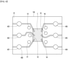
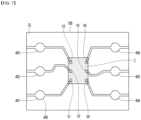
- FIGS. 2 to 5 are top views of one surface and the other surface of a smart IC substrate according to an embodiment.
- the smart IC substrate 1200 includes one surface and the other surface opposite to the one surface.
- a chip is mounted on the smart IC substrate 1200. Accordingly, a smart IC module may be provided.
- the one surface may be a contact side of the smart IC substrate 1200.
- the other surface may be a bonding side of the smart IC substrate 1200.
- the one surface may recognize information of the smart IC module through direct or indirect contact with the IC card.
- the other surface may be a surface on which a chip is mounted and adhered to the card body 2000.
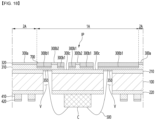
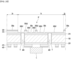
- the smart IC substrate 1200 includes a substrate 100 and a plurality of circuit patterns.
- the substrate 100 may include a resin material.
- the substrate 100 may include a first surface 1S and a second surface 2S opposite to the first surface 1S.
- the first surface 1S may be one surface of the smart IC substrate 1200. That is, the first surface 1S may be defined as a surface corresponding to the contact side of the smart IC substrate 1200. Also, the second surface 2S may be defined as a surface corresponding to the bonding side of the smart IC substrate 1200.
- the substrate 100 may include a prepreg including a glass fiber.
- the substrate 100 may include an epoxy resin and a material in which a glass fiber and a silicon-based filler are dispersed in the epoxy resin.
- the substrate 100 may be rigid or flexible.
- the substrate 100 may include glass or plastic.
- the substrate 100 may include chemical-enhanced/semi-enhanced glass such as soda time glass or aluminosilicate glass, or may include polyimide (PI), polyethylene terephthalate (PET), propylene glycol (PPG), polycarbonate (PC), etc., or may include sapphire.
- PI polyimide
- PET polyethylene terephthalate
- PPG propylene glycol
- PC polycarbonate
- the substrate 100 may include a photo isotropic film.
- the substrate 100 may include a cyclic olefin copolymer (COC), a cyclic olefin polymer (COP), a photo isotropic polycarbonate (PC), a photo isotropic polymethyl methacrylate (PMMA), or the like.
- COC cyclic olefin copolymer
- COP cyclic olefin polymer
- PC photo isotropic polycarbonate
- PMMA photo isotropic polymethyl methacrylate
- the substrate 100 may be partially bent having a curved surface. That is, the substrate 100 may bent while partially having a flat surface and partially having a curved surface. In detail, an end of the substrate 100 may be bent having a curved surface or may be curved or bent having a surface including a random curvature.
- the substrate 100 may be a flexible substrate having a flexible characteristic. Also, the substrate 100 may be a curved or bent substrate.
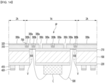
- Adhesive layers 210 and 220 are disposed on the first surface 1S and the second surface 2S.
- the adhesive layers 210 and 220 may be disposed on an entire surface of the first surface 1S and the second surface 2S.
- the adhesive layers 210 and 220 may be disposed on the front surface of the first surface 1S and the second surface 2S, except for a region in which a via is formed.
- the adhesive layers 210 and 220 may include a resin material.
- the adhesive layers 210 and 220 may include at least one of an epoxy resin, an acrylic resin, and a polyimide resin.
- the adhesive layers 210 and 220 may further include additives such as natural rubber, a plasticizer, a curing agent, and a flame retardant such as phosphorus.
- circuit patterns 300 and 400 are disposed on the substrate 100.
- circuit patterns may be disposed on the first surface 1S and the second surface 2S, respectively.
- a first circuit pattern 300 may be disposed on the first surface 1S
- a second circuit pattern 400 may be disposed on the second surface 2S. That is, the first circuit pattern 300 may be disposed on a contact side of the smart IC substrate.
- the second circuit pattern 400 may be disposed on a bonding side of the smart IC substrate.
- the first circuit pattern 300 may be disposed on the first adhesive layer 210 disposed on the substrate 100.
- the first circuit pattern 300 may include a first metal layer 310 and a second metal layer 320. Specifically, the first circuit pattern 300 may include a first metal layer 310 disposed on the first adhesive layer 210 and a second metal layer 320 disposed on the first metal layer 310.
- the first metal layer 310 includes a metal material.
- the first metal layer 310 may include a metal material having high electrical conductivity.
- the first metal layer 310 may include at least one of gold (Au), silver (Ag), platinum (Pt), titanium (Ti), tin (Sn), copper (Cu), and zinc (Zn).
- the first metal layer 310 may include copper (Cu).
- the second metal layer 320 may be disposed on the first metal layer 310. Accordingly, the second metal layer 320 may protect the first metal layer 310. That is, the second metal layer 320 may prevent corrosion of the first metal layer 310. That is, the second metal layer 320 may be a protective layer that protects the first circuit pattern 300.
- the second metal layer 320 may include nickel-gold (Ni-Au) or nickel-palladium (Ni-Pd). However, the embodiment is not limited thereto.
- the second metal layer 320 may form a nickel (Ni) layer on the first metal layer 310, and then a gold (Au) layer may be disposed on the nickel layer.
- the second metal layer 320 may be formed by forming a nickel layer on the first metal layer 310 and then disposing a palladium layer on the nickel layer.
- a nickel-gold alloy layer may be formed between the nickel layer and the gold layer.
- a nickel-palladium alloy layer may be formed between the nickel layer and the palladium layer.
- the first metal layer 310, the second metal layer 320, and the first adhesive layer 210 may have different thicknesses.
- a thickness of the first metal layer 310 may be greater than a thickness of the second metal layer 320 and a thickness of the first adhesive layer 210. Also, a thickness of the first adhesive layer 210 may be greater than a thickness of the second metal layer 320.
- the first metal layer 310 may have a thickness of 35 to 70 ⁇ m
- the second metal layer 320 may have a thickness of 1 to 3 ⁇ m
- the first active layer 210 may have a thickness of 15 to 30 ⁇ m.
- the second circuit pattern 400 is disposed on the second active layer 210 disposed on the substrate 100.
- the second circuit pattern 400 may include a third metal layer 410 and a fourth metal layer 420. Specifically, the second circuit pattern 400 may include a third metal layer 410 disposed on the second adhesive layer 220 and a fourth metal layer 420 disposed on the third metal layer 410.
- the third metal layer 410 includes a metal material.
- the third metal layer 410 may include a metal material having high electrical conductivity.
- the third metal layer 330 may include at least one of gold (Au), silver (Ag), platinum (Pt), titanium (Ti), tin (Sn), copper (Cu), and zinc (Zn).
- the third metal layer 330 may include copper (Cu).
- the fourth metal layer 420 may be disposed on the third metal layer 410.
- the fourth metal layer 420 may protect the third metal layer 410. That is, the fourth metal layer 420 may prevent corrosion of the third metal layer 410. That is, the fourth metal layer 420 may be a protective layer that protects the second circuit pattern 400.
- the fourth metal layer 420 may include the same or different metal materials among metal materials included in the second metal layer 320 described above.
- the third metal layer 410, the fourth metal layer 420, and the second adhesive layer 220 may have different thicknesses.
- a thickness of the third metal layer 410 may be greater than a thickness of the fourth metal layer 420 and a thickness of the second adhesive layer 220. Also, a thickness of the second adhesive layer 220 may be greater than a thickness of the fourth metal layer 420.
- the thickness of the third metal layer 410 may be 35 to 70 ⁇ m.
- the thickness of the fourth metal layer 420 may be 3 to 8 ⁇ m.
- the thickness of the second adhesive layer 220 may be 15 to 30 ⁇ m.
- the thickness of the fourth metal layer 420 may be greater than the thickness of the second metal layer 320. That is, the fourth metal layer 420 disposed on the bonding side of the smart IC substrate 1200 may be greater than the thickness of the second metal layer 320.
- the first circuit pattern 300 includes a plurality of circuit patterns. Specifically, the first circuit pattern 300 may include a plurality of circuit patterns spaced apart from each other.
- the first circuit pattern 300 may include a first-first circuit pattern 301, a first-second circuit pattern 302, a first-third circuit pattern 303, a first-fourth circuit pattern 304, a first-fifth circuit pattern 305, and a first-sixth circuit pattern 306.
- the first-first circuit pattern 301, the first-second circuit pattern 302, the first-third circuit pattern 303, the first-fourth circuit pattern 304, the first-fifth circuit pattern 305, and the first-sixth circuit pattern 306 are illustrated, but an embodiment is not limited thereto.
- the first circuit pattern 300 may include less than six circuit patterns or more than six circuit patterns.
- the first-first circuit pattern 301, the first-second circuit pattern 302, the first-third circuit pattern 303, the first-fourth circuit pattern 304, the first-fifth circuit pattern 305, and the first-sixth circuit pattern 306 may be spaced apart from each other.
- space regions SA in which a circuit pattern is not disposed are formed between the first-first circuit pattern 301, the first-second circuit pattern 302, the first-third circuit pattern 303, the first-fourth circuit pattern 304, the first-fifth circuit pattern 305, and the first-sixth circuit pattern 306.
- the first-first circuit pattern 301, the first-second circuit pattern 302, the first-third circuit pattern 303, the first-fourth circuit pattern 304, the first-fifth circuit pattern 305, and the first-sixth circuit pattern 306 may be spaced apart from each other.
- the spacer region SA may be a spacing between the first-first circuit pattern 301, the first-second circuit pattern 302, the first-third circuit pattern 303, the first-fourth circuit pattern 304, the first-fifth circuit pattern 305, and the first-sixth circuit pattern 306.
- the spacer region SA may have a predetermined size.
- the spacer region SA may be in a range of 100 ⁇ m to 250 ⁇ m.
- the first-first circuit pattern 301, the first-second circuit pattern 302, the first-third circuit pattern 303, the first-fourth circuit pattern 304, the first-fifth circuit pattern 305, and the first-sixth circuit pattern 306 are not electrically connected on the first surface 1S of the substrate 100.
- the second circuit pattern 400 may include a second-first circuit pattern 401, a second-second circuit pattern 402, a second-third circuit pattern 403, a second-fourth circuit pattern 404, a second-fifth circuit pattern 405, and a second-sixth circuit pattern 406.
- the second-first circuit pattern 401, the second-second circuit pattern 402, the second-third circuit pattern 403, the second-fourth circuit pattern 404, the second-fifth circuit pattern 405, and the second-sixth circuit pattern 406 are illustrated, but an embodiment is not limited thereto.
- the second circuit pattern 400 may include less than six circuit patterns or more than six circuit patterns.
- the second-first circuit pattern 401, the second-second circuit pattern 402, the second-third circuit pattern 403, the second-fourth circuit pattern 404, the second-fifth circuit pattern 405, and the second-sixth circuit pattern 406 may be spaced apart from each other.
- a chip mounting region may be formed on the second-first circuit pattern 401, the second-second circuit pattern 402, the second-third circuit pattern 403, the second-fourth circuit pattern 404, the second-fifth circuit pattern 405, and the second-sixth circuit pattern 406 disposed on the second surface 2S of the substrate 100.
- a chip C electrically connected to the first circuit pattern 300 and the second circuit pattern 400 is disposed in the chip mounting region. Accordingly, the smart IC module may be formed.
- the chip C may be disposed on the second circuit pattern 400 and may be connected to the second circuit pattern 400. That is, the chip C is in direct contact with the second circuit pattern 400. Accordingly, the chip C may be electrically connected to the second circuit pattern 400.
- the chip C may be connected to the first circuit pattern 300.
- At least one via hole may be formed to connect the chip C to the first circuit pattern 300.
- a plurality of via holes passing through the first surface 1S and the second surface 2S may be formed in the substrate 100.
- a plurality of via holes may be formed in the substrate 100.
- a plurality of via holes corresponding to each of the first circuit patterns 300 may be formed in the substrate 100.
- the first via hole V1 may be formed in a region overlapping the first-first circuit pattern 301 in a thickness direction of the substrate 100.
- the second via hole V2 may be formed in a region overlapping the first-second circuit pattern 302 in the thickness direction of the substrate 100.
- the third via hole V3 may be formed in a region overlapping the first-third circuit pattern 303 in the thickness direction of the substrate 100.
- the fourth via hole V4 may be formed in a region overlapping the first-fourth circuit pattern 304 in the thickness direction of the substrate 100.
- the fifth via hole V5 may be formed in a region overlapping the first-fifth circuit pattern 305 in the thickness direction of the substrate 100.
- a sixth via hole V6 may be formed in a region overlapping the first-sixth circuit pattern 306 in the thickness direction of the substrate 100.
- the chip C and the first circuit pattern 300 may be connected by a wire bonding. That is, the chip C and the first circuit pattern may be electrically connected through a plurality of wires 500 passing through the via hole.
- a pad part 350 for wire bonding may be disposed on the first circuit pattern 300.
- the first circuit pattern 300 and the second circuit pattern 400 may be electrically connected through the conductive layer 800 inside the via hole passing through the substrate 100.
- a plurality of via holes may be formed in the substrate 100.
- a plurality of via holes corresponding to each of the first circuit patterns 300 may be formed in the substrate 100.
- the first via hole V1 may be formed in a region overlapping the first-first circuit pattern 301 in a thickness direction of the substrate 100.
- the second via hole V2 may be formed in a region overlapping the first-second circuit pattern 302 in the thickness direction of the substrate 100.
- the third via hole V3 may be formed in a region overlapping the first-third circuit pattern 303 in the thickness direction of the substrate 100.
- the fourth via hole V4 may be formed in a region overlapping the first-fourth circuit pattern 304 in the thickness direction of the substrate 100.
- the fifth via hole V5 may be formed in a region overlapping the first-fifth circuit pattern 305 in the thickness direction of the substrate 100.
- a sixth via hole V6 may be formed in a region overlapping the first-sixth circuit pattern 306 in the thickness direction of the substrate 100.
- a plating layer 600 may be disposed on an inner surface of the first via hole V1, the second via hole V2, the third via hole V3, the fourth via hole V4, the fifth via hole V5, and the sixth via hole V6.
- the plating layer 600 may be connected to the first circuit pattern 300 and the second circuit pattern 400. Accordingly, the chip C may be electrically connected to the first circuit pattern 300 and the second circuit pattern 400.
- the smart IC substrate 1200 may include an identification pattern IP capable of identifying information of the IC card.
- the identification pattern IP may be disposed on the first surface 1S of the substrate 100. More specifically, the identification pattern IP may be disposed on the contact side of the smart IC substrate 1200.
- a first region 1A in which the identification pattern IP is disposed and a second region 2A other than the first region 1A may be defined in the substrate 100.
- the identification pattern IP may be disposed in the first region 1A.
- the user may identify the information of the IC card through the contact side exposed to the outside of the IC card.
- the identification pattern IP may be formed by the first circuit pattern 300. Specifically, the identification pattern IP may be formed by partially etching the first circuit pattern 300. That is, the identification pattern IP may be a part of the first circuit pattern 300. That is, the identification pattern IP may be a partial region of the first circuit pattern 300.
- the identification pattern IP may be formed by various methods. Specifically, the identification pattern IP may be formed in various shapes according to an etching method of the first circuit pattern 300.
- the identification pattern of the smart IC substrate according to a first embodiment will be described with reference to FIGS. 2 , 6 to 9 .
- the first circuit pattern 300 may be defined as a first circuit pattern part 300a, a second circuit pattern part 300b, and a third circuit pattern part 300c.
- the thicknesses of the first circuit pattern part 300a, the second circuit pattern part 300b, and the third circuit pattern part 300c may be different from each other.
- the thickness of the first circuit pattern part 300a may be greater than the thicknesses of the second circuit pattern part 300b and the third circuit pattern part 300c.
- the thickness of the second circuit pattern part 300b may be greater than the thickness of the third circuit pattern part 300c.
- the first circuit pattern part 300a may include the first metal layer 310 and the second metal layer 320.
- the first circuit pattern part 300a may be a region in which the first circuit pattern 300 is not etched.
- the first circuit pattern part 300a may be disposed in at least one of the first region 1A and the second region 2A. Specifically, the first circuit pattern part 300a may be disposed in both the first region 1A and the second region 2A.
- the second circuit pattern part 300b may include the first metal layer 310 and the second metal layer 320.
- the second circuit pattern part 300b may be disposed in the first region 1A. Specifically, the second circuit pattern part 300b may be disposed only in the first region 1A.
- thicknesses of the first metal layer 310 of the first circuit pattern part 300a and the first metal layer 310 of the second circuit pattern part 300b may be different. Specifically, the first metal layer 310 of the first circuit pattern part 300a may be greater than the thickness of the first metal layer 310 of the second circuit pattern part 300b.
- the first circuit pattern part 300a and the second circuit pattern part 300b may have a thickness difference due to a thickness difference between the first metal layer 310.
- the thickness of the second circuit pattern part 300b may be 10% to 50% of the thickness of the first circuit pattern part 300a. Forming the thickness of the second circuit pattern part 300b to exceed 50% of the thickness of the first circuit pattern part 300a may be difficult to implement in an etching process. Also, when the thickness of the second circuit pattern part 300b is less than 10% of the thickness of the first circuit pattern part 300a, the thickness of the first metal layer 310 of the second circuit pattern part 300b may be reduced, thereby reducing conductivity.
- the difference in thickness between the first circuit pattern part 300a and the second circuit pattern part 300b may be 3.5 ⁇ m to 18 ⁇ m. Forming the difference in thickness between the first circuit pattern part 300a and the second circuit pattern part 300b to be less than 3.5 ⁇ m may be difficult to implement in an etching process. Also, when the difference in thickness between the first circuit pattern part 300a and the second circuit pattern part 300b exceeds 18 ⁇ m, the thickness of the first metal layer 310 of the second circuit pattern part 300b may be reduced, thereby reducing conductivity.
- the width of the second circuit pattern part 300b may be similar to or greater than a width of the space region SA.
- the second circuit pattern part 300b may be a region in which the first circuit pattern 300 is etched. Specifically, the second circuit pattern part 300b may be a region in which the first metal layer 310 of the first circuit pattern 300 is partially etched.
- the second circuit pattern part 300b may correspond to the identification pattern IP. That is, a pattern including texts, symbols, or numbers may be formed on the smart IC substrate 1200 by the second circuit pattern part 300b. That is, an identification pattern IP including texts, symbols, or numbers of an engraved shape may be formed on the smart IC substrate 1200. That is, an identification pattern IP including texts, symbols, or numbers of an engraved shape may be formed on the smart IC substrate 1200.
- the second circuit pattern part 300b may be disposed at a position overlapping the via holes V1, V2, V3, V4, V5, and V6. Specifically, the second circuit pattern part 300b may be disposed at a position overlapping the via holes V1, V2, V3, V4, V5, and V6 in a thickness direction of the substrate 120.
- the second circuit pattern part 300b may be disposed at a position that does not overlap the via holes V1, V2, V3, V4, V5, and V6. Specifically, the second circuit pattern part 300b may be disposed at a position that does not overlap the via holes V1, V2, V3, V4, V5, and V6 in a thickness direction of the substrate 100.
- the second circuit pattern part 300b may be disposed in at least one of a position that overlaps or a position that does not overlap the via holes V1, V2, V3, V4, V5, and V6 in the thickness direction of the substrate 100.
- the second circuit pattern part 300b may be disposed in a position that overlaps and a position that does not overlap the via holes V1, V2, V3, V4, V5, and V6 in the thickness direction of the substrate 100.
- the position of the second circuit pattern part 300b may be disposed regardless of the positions of the via holes V1, V2, V3, V4, V5, and V6. That is, the identification pattern IP formed by the second circuit pattern part 300b may be disposed regardless of the positions of the via holes V1, V2, V3, V4, V5, and V6.
- identification patterns when the identification pattern is formed on the IC card, identification patterns may be formed at various positions regardless of the position of the via hole formed in the substrate. Accordingly, the degree of design freedom of the identification pattern may be improved.
- the first circuit pattern part 300a and the second circuit pattern part 300b may be recognized as different colors. Specifically, the first circuit pattern part 300a and the second circuit pattern part 300b may have different thicknesses due to the difference in thickness of the first metal layer 310. Accordingly, a contrast difference occurs between the first circuit pattern part 300a and the second circuit pattern part 300b due to the thickness difference. Accordingly, a user can recognize the first circuit pattern part 300a and the second circuit pattern part 300b as different colors from the outside due to the contrast difference.
- the degree of design freedom may be improved. Also, since the first circuit pattern part 300a and the second circuit pattern part 300b are distinguished by a difference in thickness or color, the user can easily identify the identification pattern of the IC card from the outside.
- the third circuit pattern part 300c may be a region in which the first circuit pattern 300 is etched. Specifically, the third circuit pattern part 300c may be a region in which the first circuit pattern 300 is completely or almost etched. That is, the first circuit pattern 300 may not remain in the third circuit pattern part 300c or may remain in a small amount. That is, the thickness of the first circuit pattern 300 in the third circuit pattern part 300c may be zero or close to zero.
- the meaning that the third circuit pattern part 300c remains may mean that the first circuit pattern 300 is not connected to adjacent circuit patterns on the first surface 1S of the substrate 100 after etching. Additionally, it means that it remains in an amount such that a plating layer is not formed by the plating process.
- the third circuit pattern part 300c may correspond to the space region SA. That is, the third circuit pattern part 300c may be the space region SA. That is, the first circuit pattern 300 may be divided into a plurality of circuit patterns by the third circuit pattern part 300c.
- the first circuit pattern 300 may be defined as a first circuit pattern part 300a, a second-first circuit pattern part 300b1, a second-second circuit pattern part 300b2, and a third circuit pattern part 300c.
- Thicknesses of the first circuit pattern part 300a, the second-first circuit pattern part 300b1, the second-second circuit pattern part 300b2, and the third circuit pattern part 300c may be different from each other.
- the thickness of the first circuit pattern part 300a may be greater than the thicknesses of the second-first circuit pattern part 300b1 and the third circuit pattern part 300c.
- the thickness of the second-first circuit pattern part 300b1 may be greater than the thickness of the third circuit pattern part 300c. Also, the thicknesses of the first circuit pattern part 300a and the second-second circuit pattern part 300b2 may be the same or may be the same within a tolerance range. Also, the thickness of the second-second circuit pattern part 300b2 may be greater than the thickness of the second-first circuit pattern part 300b1.
- the first circuit pattern part 300a may include the first metal layer 310 and the second metal layer 320.
- the first circuit pattern part 300a may be a region in which the first circuit pattern 300 is not etched.
- the first circuit pattern part 300a may be disposed in the second region 2A. Specifically, the first circuit pattern part 300a may be disposed only in the second region 2A.
- the second-first circuit pattern part 300b1 may include the first metal layer 310 and the second metal layer 320.
- the second-first circuit pattern part 300b1 may be disposed in the first region 1A. Specifically, the second-first circuit pattern part 300b1 may be disposed only in the first region 1A.
- thicknesses of the first metal layer 310 of the first circuit pattern part 300a and the first metal layer 310 of the second-first circuit pattern part 300b1 may be different from each other. Specifically, the first metal layer 310 of the first circuit pattern part 300a may be greater than the thickness of the first metal layer 310 of the second-first circuit pattern part 300b1.
- the first circuit pattern part 300a and the second-first circuit pattern part 300b1 may have different thicknesses due to the difference in thickness of the first metal layer 310.
- the thickness of the second-first circuit pattern part 300b1 may be 10% to 50% of the thickness of the first circuit pattern part 300a.
- the thickness of the second-first circuit pattern part 300b1 exceeds 50% of the thickness of the first circuit pattern part 300a, it may be difficult to implement in the etching process.
- the thickness of the second-first circuit pattern part 300b1 is less than 10% of the thickness of the first circuit pattern part 300a, the thickness of the first metal layer 310 of the second-first circuit pattern part 300b1 may be reduced, thereby reducing conductivity.
- the difference in thickness between the first circuit pattern part 300a and the second-first circuit pattern part 300b1 may be 3.5 ⁇ m to 18 ⁇ m.
- the difference in thickness between the first circuit pattern part 300a and the second-first circuit pattern part 300b1 is less than 3.5 ⁇ m, it may be difficult to implement in the etching process.
- the difference in thickness between the first circuit pattern part 300a and the second-first circuit pattern part 300b1 exceeds 18 ⁇ m, the thickness of the first metal layer 310 of the second-first circuit pattern part 300b1 may be reduced, thereby reducing conductivity.
- a width of the second-first circuit pattern part 300b1 may be similar to or greater than a width of the space region SA.
- the second-first circuit pattern part 300b1 may be a region in which the first circuit pattern 300 is etched. Specifically, the second-first circuit pattern part 300b1 may be a region in which the first metal layer 310 of the first circuit pattern 300 is partially etched.
- the second-first circuit pattern part 300b1 may be disposed at a position overlapping the via holes V1, V2, V3, V4, V5, and V6. Specifically, the second-first circuit pattern part 300b1 may be disposed at a position overlapping the via holes V1, V2, V3, V4, V5, and V6 in a thickness direction of the substrate 100.
- the second-first circuit pattern part 300b1 may be disposed at a position that does not overlap the via holes V1, V2, V3, V4, V5, and V6. Specifically, the second-first circuit pattern part 300b1 may be disposed at a position that does not overlap the via holes V1, V2, V3, V4, V5, and V6 in a thickness direction of the substrate 100.
- the second-first circuit pattern part 300b1 may be disposed at both a position that does not overlap the via holes V1, V2, V3, V4, V5, and V6 and a position that does not overlap the via holes V1, V2, V3, V4, V5, and V6 in a thickness direction of the substrate 100. In other words, the second-first circuit pattern part 300b1 may be disposed regardless of the positions of the via holes V1, V2, V3, V4, V5, and V6.
- the first circuit pattern part 300a and the second-first circuit pattern part 300b1 may be recognized as different colors. Specifically, the first circuit pattern part 300a and the second-first circuit pattern part 300b1 may have different thicknesses due to the difference in thickness of the first metal layer 310. Accordingly, the difference in contrast occurs between the first circuit pattern part 300a and the second-first circuit pattern part 300b1 due to the difference in thickness. Accordingly, a user may recognize the first circuit pattern part 300a and the second-first circuit pattern part 300b1 as different colors from the outside due to the difference in contrast.
- the degree of design freedom may be improved. Also, since the first circuit pattern part 300a and the second-first circuit pattern part 300b1 are distinguished by a difference in thickness or color, the user can easily identify the identification pattern of the IC card from the outside.
- the second-second circuit pattern part 300b2 may include the first metal layer 310 and the second metal layer 320.
- the second-second circuit pattern part 300b2 may be a region in which the first circuit pattern 300 is not etched.
- the second-second circuit pattern part 300b2 may be disposed in the first region 1A. Specifically, the second-second circuit pattern part 300b2 may be disposed only in the first region 1A.
- the second-first circuit pattern part 300b1 and the second-second circuit pattern part 300b2 may be disposed in the first region 1A in which the identification pattern IP is formed.
- an identification pattern IP may be formed in the first region 1A by the second-first circuit pattern part 300b1 and the second-second circuit pattern part 300b2.
- an identification pattern IP may be formed in the first region 1A by the second-first circuit pattern part 300b1 and the second-second circuit pattern part 300b2 of the first circuit pattern 300 having different thicknesses.
- a pattern including texts, symbols, or numbers may be formed on the smart IC substrate 1200 by the second-first circuit pattern part 300b1 and the second-second circuit pattern part 300b2. That is, an identification pattern IP including embossed texts, symbols, or numbers may be formed on the smart IC substrate 1200.
- the color of the second-first circuit pattern part 300b1 may be recognized as a different color of at least one of the first circuit pattern part 300a and the second-second circuit pattern part 300b2.
- the second-first circuit pattern part 300b1 and the second-second circuit pattern part 300b2 may be recognized as different colors.
- the first circuit pattern part 300a and the second-first circuit pattern part 300b1 may have different thicknesses due to the difference in thickness of the first metal layer 310. Accordingly, the difference in contrast occurs between the first circuit pattern part 300a and the second-first circuit pattern part 300b1 due to the difference in thickness. Accordingly, the user can recognize the first circuit pattern part 300a and the second-first circuit pattern part 300b1 as different colors from the outside due to the difference in contrast.
- the second-first circuit pattern part 300b1 and the second-second circuit pattern part 300b2 are distinguished by a difference in thickness or color, the user can easily identify the identification pattern of the IC card from the outside.
- the user can recognize the identification pattern IP as two or more colors, thereby improving the degree of freedom in external design of the identification pattern.
- the second-first circuit pattern part 300b1 may be disposed in the first region 1A regardless of the positions of the via holes V1, V2, V3, V4, V5, and V6. Accordingly, the identification pattern IP formed by the second-first circuit pattern part 300b1 and the second-second circuit pattern part 300b2 may also be disposed regardless of the positions of the via holes V1, V2, V3, V4, V5, and V6.
- identification patterns when the identification pattern is formed on the IC card, identification patterns may be formed at various positions regardless of the position of the via hole formed in the substrate. Accordingly, the degree of design freedom of the identification pattern may be improved.
- the third circuit pattern part 300c may be a region in which the first circuit pattern 300 is etched. Specifically, the third circuit pattern part 300c may be a region in which the first circuit pattern 300 is completely or almost etched. That is, the first circuit pattern 300 may not remain in the third circuit pattern part 300c or may remain in a small amount. That is, the thickness of the first circuit pattern 300 disposed on the third circuit pattern part 300c may be zero or close to zero.
- the meaning that the third circuit pattern part 300c remains means that the first circuit pattern 300 is not connected to adjacent circuit patterns on the first surface 1S of the substrate 100 after etching. Additionally, it means that it remains in an amount such that a plating layer is not formed by the plating process.
- the third circuit pattern part 300c may correspond to the space region SA. That is, the third circuit pattern part 300c may be the space region SA. That is, the first circuit pattern 300 may be divided into a plurality of circuit patterns by the third circuit pattern part 300c.
- the first circuit pattern 300 may include a first circuit pattern part 300a, a second-first circuit pattern part 300b1, a second-second circuit pattern part 300b2, and a third circuit pattern part 300c.
- the thicknesses of the first circuit pattern part 300a, the second-first circuit pattern part 300b1, the second-second circuit pattern part 300b2, and the third circuit pattern part 300c may be different from each other.
- the thickness of the first circuit pattern part 300a may be greater than the thicknesses of the second-first circuit pattern part 300b1, the second-second circuit pattern part 300b2, and the third circuit pattern part 300c.
- the thickness of the second-second circuit pattern part 300b2 may be greater than the thickness of the second-first circuit pattern part 300b1 and the third circuit pattern part 300c.
- the thickness of the second-first circuit pattern part 300b1 may be greater than the thickness of the third circuit pattern part 300c.
- the first circuit pattern part 300a may include the first metal layer 310 and the second metal layer 320.
- the first circuit pattern part 300a may be a region in which the first circuit pattern 300 is not etched.
- the first circuit pattern part 300a may be disposed in the second region 2A. Specifically, the first circuit pattern part 300a may be disposed only in the second region 2A.
- the second-first circuit pattern part 300b1 may include the first metal layer 310 and the second metal layer 320.
- the second-first circuit pattern part 300b1 may be disposed in the first region 1A. Specifically, the second-first circuit pattern part 300b1 may be disposed only in the first region 1A.
- thicknesses of the first metal layer 310 of the first circuit pattern part 300a and the first metal layer 310 of the second-first circuit pattern part 300b1 may be different from each other. Specifically, the first metal layer 310 of the first circuit pattern part 300a may be greater than the thickness of the first metal layer 310 of the second-first circuit pattern part 300b1.
- the first circuit pattern part 300a and the second-first circuit pattern part 300b1 may have different thicknesses according to the difference in thickness of the first metal layer 310.
- the thickness of the second-first circuit pattern part 300b1 may be 10% to 50% of the thickness of the first circuit pattern part 300a.
- the thickness of the second-first circuit pattern part 300b1 exceeds 50% of the thickness of the first circuit pattern part 300a, it may be difficult to implement in the etching process.
- the thickness of the second-first circuit pattern part 300b1 is less than 10% of the thickness of the first circuit pattern part 300a, the thickness of the first metal layer 310 of the second-first circuit pattern part 300b1 may be reduced, thereby reducing conductivity.
- the difference in thickness between the first circuit pattern part 300a and the second-first circuit pattern part 300b may be 3.5 ⁇ m to 18 ⁇ m.
- the difference in thickness between the first circuit pattern part 300a and the second-first circuit pattern part 300b1 is less than 3.5 ⁇ m, it may be difficult to implement in the etching process.
- the difference in thickness between the first circuit pattern part 300a and the second-first circuit pattern part 300b1 exceeds 18 ⁇ m, the thickness of the first metal layer 310 of the second-first circuit pattern part 300b1 may be reduced, thereby reducing conductivity.
- the width of the second-first circuit pattern part 300b1 may be similar to or greater than a width of the space region SA.
- the second-first circuit pattern part 300b1 may be a region in which the first circuit pattern 300 is etched. Specifically, the second-first circuit pattern part 300b1 may be a region in which the first metal layer 310 of the first circuit pattern 300 is partially etched.
- the second-first circuit pattern part 300b1 may be disposed at a position overlapping the via holes V1, V2, V3, V4, V5, and V6. Specifically, the second-first circuit pattern part 300b1 may be disposed at a position overlapping the via holes V1, V2, V3, V4, V5, and V6 in a thickness direction of the substrate 100.
- the second-first circuit pattern part 300b1 may be disposed at a position that does not overlap the via holes V1, V2, V3, V4, V5, and V6. Specifically, the second-first circuit pattern part 300b1 may be disposed at a position that does not overlap the via holes V1, V2, V3, V4, V5, and V6 in a thickness direction of the substrate 100.
- the second-first circuit pattern part 300b1 may be disposed at both a position that does not overlap the via holes V1, V2, V3, V4, V5, and V6 and a position that does not overlap the via holes V1, V2, V3, V4, V5, and V6 in a thickness direction of the substrate 100. In other words, the second-first circuit pattern part 300b1 may be disposed regardless of the positions of the via holes V1, V2, V3, V4, V5, and V6.
- the first circuit pattern part 300a and the second-first circuit pattern part 300b1 may be recognized as different colors. Specifically, the first circuit pattern part 300a and the second-first circuit pattern part 300b1 may have different thicknesses due to the difference in thickness of the first metal layer 310. Accordingly, the difference in contrast occurs between the first circuit pattern part 300a and the second-first circuit pattern part 300b1 due to the difference in thickness. Accordingly, a user can recognize the first circuit pattern part 300a and the second-first circuit pattern part 300b1 as different colors from the outside due to the difference in contrast.
- the degree of design freedom of the first surface 1S exposed to the outside of the IC card may be improved.
- the second-second circuit pattern part 300b2 may include the first metal layer 310 and the second metal layer 320.
- the second-second circuit pattern part 300b2 may be a region in which the first circuit pattern 300 is etched.
- the second-second circuit pattern part 300b2 may be a region in which the first metal layer 310 of the first circuit pattern 300 is partially etched.
- the thickness of the first metal layer 310 of the second-second circuit pattern part 300b2 may be greater than the thickness of the first metal layer 310 of the second-first circuit pattern part 300b1. That is, the thickness of the first metal layer 310 of the first circuit pattern part 300a may be greater than the thickness of the first metal layer 310 of the second-second circuit pattern part 300b2. In addition, the thickness of the first metal layer 310 of the second-second circuit pattern part 300b2 may be greater than the thickness of the first metal layer 310 of the second-first circuit pattern part 300b1.
- the difference between the thickness of the first metal layer 310 of the first circuit pattern part 300a and the thickness of the first metal layer 310 of the second-first circuit pattern part 300b1 may be greater than or equal to the difference between the thickness of the first metal layer 310 of the second-second circuit pattern part 300b2 and the thickness of the second-first circuit pattern part 300b1.
- the second-second circuit pattern part 300b2 may be disposed in the first region 1A. Specifically, the second-second circuit pattern part 300b2 may be disposed only in the first region 1A.
- the second-first circuit pattern part 300b1 and the second-second circuit pattern part 300b2 may be disposed in the first region 1A in which the identification pattern IP is formed.
- an identification pattern IP may be formed in the first region 1A by the second-first circuit pattern part 300b1 and the second-second circuit pattern part 300b2.
- an identification pattern IP may be formed in the first region 1A by the second-first circuit pattern part 300b1 and the second-second circuit pattern part 300b2 of the first circuit pattern 300 having different thicknesses.
- a pattern including texts, symbols, or numbers may be formed on the smart IC substrate 1200 by the second-first circuit pattern part 300b1 and the second-second circuit pattern part 300b2. That is, an identification pattern IP including embossed texts, symbols, or numbers may be formed on the smart IC substrate 1200.
- the second-first circuit pattern part 300b1 and the second-second circuit pattern part 300b2 may be recognized as different colors.
- the first circuit pattern part 300a and the second-first circuit pattern part 300b1 may have different thicknesses due to the difference in thickness of the first metal layer 310. Accordingly, a difference in contrast occurs between the first circuit pattern part 300a and the second-first circuit pattern part 300b1 due to a difference in thickness. Accordingly, the user can recognize the first circuit pattern part 300a and the second-first circuit pattern part 300b1 as different colors from the outside due to the difference in contrast.
- the second-first circuit pattern part 300b1 and the second-second circuit pattern part 300b2 are distinguished by a difference in thickness or color, the user can easily identify the identification pattern of the IC card from the outside.
- the user can recognize at least three or more colors from the outside. Accordingly, the degree of freedom in external design of the IC card can be improved.
- the second-first circuit pattern part 300b1 may be disposed in the first region 1A regardless of the positions of the via holes V1, V2, V3, V4, V5, and V6. Accordingly, the identification pattern IP formed by the second-first circuit pattern part 300b1 and the second-second circuit pattern part 300b2 may also be disposed regardless of the positions of the via holes V1, V2, V3, V4, V5, and V6.
- identification patterns when the identification pattern is formed on the IC card, identification patterns may be formed at various positions regardless of the position of the via hole formed in the substrate. Accordingly, the degree of design freedom of the identification pattern may be improved.
- the thickness of both the second-first circuit pattern part 300b1 and the second-second circuit pattern part 300b2 disposed in the first region 1A may be smaller than the thickness of the first circuit pattern part 300a disposed in the second region 2A.
- a difference in contrast due to a difference in thickness may occur in the first region 1A and the second region 2A. That is, a difference in contrast may occur due to a difference in thickness between the second-second circuit pattern part 300b2 and the thickness of the first circuit pattern part 300a having the shape of an identification pattern IP in the first region 1A. Accordingly, the user can easily recognize the identification pattern IP disposed in the first region 1A from the outside. In addition, more various designs of identification patterns may be formed by using the difference in contrast.
- the third circuit pattern part 300c may be a region in which the first circuit pattern 300 is etched. Specifically, the third circuit pattern part 300c may be a region in which the first circuit pattern 300 is completely or almost etched. That is, the first circuit pattern 300 may not remain in the third circuit pattern part 300c or may remain in a small amount. That is, the thickness of the first circuit pattern 300 disposed on the third circuit pattern part 300c may be zero or close to zero.
- the meaning that the third circuit pattern part 300c remains means that the first circuit pattern 300 is not connected to adjacent circuit patterns on the first surface 1S of the substrate 100 after etching. Additionally, it means that it remains in an amount such that a plating layer is not formed by the plating process.
- the third circuit pattern part 300c may correspond to the space region SA. That is, the third circuit pattern part 300c may be the space region SA. That is, the first circuit pattern 300 may be divided into a plurality of circuit patterns by the third circuit pattern part 300c.
- the smart IC substrate according to the fourth embodiment may further include a reinforcing part 700.
- the reinforcing part 700 may be disposed on the second circuit pattern part 300b. Specifically, the reinforcing part 700 may be disposed to extend along the shape of the identification pattern IP.
- the reinforcing part 700 may include a resin material or a metal material.
- the reinforcing part 700 may be disposed on the second metal layer 320 of the second circuit pattern part 300b.
- the second metal layer 320 serves as a protective layer for preventing corrosion of the first metal layer 310. Since the first metal layer 320 is partially removed, the second circuit pattern part 300b may have a step difference from the first circuit pattern part 300a. As a result, the first metal layer 310 may be exposed from the side of the first circuit pattern part 300a. Accordingly, the first circuit pattern part 300a may be corroded by external moisture or oxygen.
- the reinforcing part 700 may be disposed on the second metal layer 310 of the second circuit pattern part 300b.
- the reinforcing part 700 may be disposed in contact with a side surface of the first circuit pattern part 300a. Accordingly, the first circuit pattern part 300a may be prevented from being corroded by the reinforcing part 700.
- the reinforcing part 700 may have a color.
- the reinforcing part 700 may include a resin material having a color.
- the reinforcing part 700 may include a metal material whose color coordinates are different from those of the first metal layer 310 and the second metal layer 320.
- the second circuit pattern part 300b having the shape of the identification pattern IP may have various colors. Accordingly, the degree of design freedom may be improved by implementing the identification pattern IP in various colors. In addition, the user can easily identify the identification pattern IP from the outside.
- the smart IC substrate according to the fifth embodiment may further include a reinforcing part 700.
- the reinforcing part 700 may be disposed on the second circuit pattern part 300b. Specifically, the reinforcing part 700 may be disposed to extend along the shape of the identification pattern IP.
- the reinforcing part 700 may include a resin material or a metal material.
- the reinforcing part 700 may be disposed on the second metal layer 320 of the second circuit pattern part 300b.
- the second metal layer 320 serves as a protective layer for preventing corrosion of the first metal layer 310. Since the first metal layer 320 is partially removed, the second circuit pattern part 300b may have a step difference from the first circuit pattern part 300a. Accordingly, the first metal layer 310 may be exposed on the side surface of the first circuit pattern part 300a. Accordingly, the first circuit pattern part 300a may be corroded by external moisture or oxygen.
- the reinforcing part 700 may be disposed on the second metal layer 310 of the second circuit pattern part 300b.
- the reinforcing part 700 may be disposed in contact with a side surface of the first circuit pattern part 300a. Accordingly, the first circuit pattern part 300a may be prevented from being corroded by the reinforcing part 700.
- the reinforcing part 700 may have a color.
- the reinforcing part 700 may include a resin material having a color.
- the reinforcing part 700 may include a metal material whose color coordinates are different from those of the first metal layer 310 and the second metal layer 320.
- the second circuit pattern part 300b having the shape of the identification pattern IP may have various colors. Accordingly, it is possible to improve the degree of design freedom by implementing the identification pattern IP in various colors. Accordingly, the user can easily identify the identification pattern IP from the outside.
- the reinforcing part 700 may be disposed to protrude. Specifically, the reinforcing part 700 may be disposed to protrude from an upper surface of the circuit pattern. Specifically, the reinforcing part 700 may be disposed to protrude from the upper surface of the first circuit pattern 300. More specifically, the reinforcing part 700 may be disposed to protrude from the upper surface of the second metal layer 320.
- the upper surface of the reinforcing part 700 may be disposed to protrude from the upper surface of the second metal layer 320. Accordingly, the reinforcing part 700 extending along the shape of the identification pattern IP may be disposed to protrude from the upper surface of the smart IC substrate 1200.
- the user can easily identify the identification pattern IP from the outside due to the difference in contrast according to the height difference between the reinforcing part 700 and the smart IC substrate 1200.
- the reinforcing part 700 extending according to the shape of the identification pattern IP, the user may recognize the identification pattern IP from the outside by not only sight but also touch. Therefore, the function of the identification pattern IP may be diversified.
- the smart IC substrate according to the sixth embodiment may further include a reinforcing part 700.
- the reinforcing part 700 may be disposed on the second circuit pattern part 300b. Specifically, the reinforcing part 700 may be disposed to extend along the shape of the identification pattern IP.
- the reinforcing part 700 may include a resin material or a metal material.
- the reinforcing part 700 may be disposed on the second metal layer 320 of the second-first circuit pattern part 300b1.
- the second metal layer 320 serves as a protective layer for preventing corrosion of the first metal layer 310. Since the first metal layer 320 is partially removed, the second-first circuit pattern part 300b1 may have a step difference from the first circuit pattern part 300a. Accordingly, the first metal layer 310 may be exposed on the side surface of the first circuit pattern part 300a. Accordingly, the first circuit pattern part 300a may be corroded by external moisture or oxygen.
- the reinforcing part 700 may be disposed on the second metal layer 310 of the second-first circuit pattern part 300b1.
- the reinforcing part 700 may be disposed in contact with a side surface of the first circuit pattern part 300a. Accordingly, the first circuit pattern part 300a may be prevented from being corroded by the reinforcing part 700.
- the reinforcing part 700 may have a color.
- the reinforcing part 700 may include a resin material having a color.
- the reinforcing part 700 may include a metal material whose color coordinates are different from those of the first metal layer 310 and the second metal layer 320.
- the second-first circuit pattern part 300b1 having the shape of the identification pattern IP may have various colors. Accordingly, the degree of design freedom may be improved by implementing the identification pattern IP in various colors. Accordingly, the user can easily identify the identification pattern IP from the outside.
- the identification pattern of the smart IC substrate according to the seventh embodiment will be described with reference to FIGS. 3 , 6 , 7 , 20 , and 21 .
- the smart IC substrate according to the seventh embodiment may further include a reinforcing part 700.
- the reinforcing part 700 may be disposed on the second circuit pattern part 300b. Specifically, the reinforcing part 700 may be disposed to extend along the shape of the identification pattern IP.
- the reinforcing part 700 may include a resin material or a metal material.
- the reinforcing part 700 may be disposed on the first metal layer 310 of the second-first circuit pattern part 300b1.
- the second metal layer 320 serves as a protective layer for preventing corrosion of the first metal layer 310. Since the first metal layer 320 is partially removed, the second-first circuit pattern part 300b1 may have a step difference from the first circuit pattern part 300a. Accordingly, the first metal layer 310 may be exposed on a side surface of the first circuit pattern part 300a. Accordingly, the first circuit pattern part 300a may be corroded by external moisture or oxygen.
- the reinforcing part 700 may be disposed on the second metal layer 310 of the second-first circuit pattern part 300b1. Also, the reinforcing part 700 may be disposed in contact with a side surface of the first circuit pattern part 300a. Accordingly, the first circuit pattern part 300a may be prevented from being corroded by the reinforcing part 700.
- the reinforcing part 700 may have a color.
- the reinforcing part 700 may include a resin material having a color.
- the reinforcing part 700 may include a metal material whose color coordinates are different from those of the first metal layer 310 and the second metal layer 320.
- the second-first circuit pattern part 300b1 having the shape of the identification pattern IP may have various colors. Accordingly, the degree of design freedom may be improved by implementing the identification pattern IP in various colors, thereby allowing the user to easily identify the identification pattern IP from the outside.
- the reinforcing part 700 may be disposed to protrude. Specifically, the reinforcing part 700 may be disposed to protrude from the upper surface of the circuit pattern. Specifically, the reinforcing part 700 may be disposed to protrude from the upper surface of the first circuit pattern 300. More specifically, the reinforcing part 700 may be disposed to protrude from the upper surface of the second metal layer 320.
- the upper surface of the reinforcing part 700 may be disposed to protrude from the upper surface of the second metal layer 320. Accordingly, the reinforcing part 700 extending along the shape of the identification pattern IP may be disposed to protrude from the upper surface of the smart IC substrate 1200.
- the user can easily identify the identification pattern IP by a difference in contrast according to the height difference between the reinforcing part 700 and the smart IC substrate 1200 from the outside.
- the reinforcing part 700 extending according to the shape of the identification pattern IP, the user may recognize the identification pattern IP from the outside by not only sight but also touch. Therefore, the function of the identification pattern IP may be diversified.
- the identification pattern of the smart IC substrate according to the eighth embodiment will be described with reference to FIGS. 2 , 6 , 7 , 22 , and 23 .
- the second circuit pattern part 300b may include only the first metal layer 310.
- the first circuit pattern 300 may be defined as a first circuit pattern part 300a, a second circuit pattern part 300b, and a third circuit pattern part 300c.
- the second circuit pattern part 300b may include only the first metal layer 310. That is, unlike the first circuit pattern part 300a, the second circuit pattern part 300b may not include the second metal layer 320.
- the smart IC substrate according to the first embodiment proceeds with a process of forming a first metal layer, a process of partially etching the first metal layer, and a process of forming a second metal layer.
- the first circuit pattern 300 of the second circuit pattern part 300b includes both the first metal layer and the second metal layer.
- the smart IC substrate according to the eighth embodiment forms both the first metal layer and the second metal layer, and then partially etching the second metal layer and the first metal layer.
- the first circuit pattern 300 of the second circuit pattern part 300b may include only the first metal layer.
- the second circuit pattern part 300b may be disposed in the first region 1A. Specifically, the second circuit pattern part 300b may be disposed only in the first region 1A.
- thicknesses of the first metal layer 310 of the first circuit pattern part 300a and the first metal layer 310 of the second circuit pattern part 300b may be different. Specifically, the first metal layer 310 of the first circuit pattern part 300a may be greater than the thickness of the first metal layer 310 of the second circuit pattern part 300b.
- the first circuit pattern part 300a and the second circuit pattern part 300b may have different thicknesses depending on the difference in thickness of the first metal layer 310 and the presence or absence of the second metal layer 320.
- the first circuit pattern part 300a and the second circuit pattern part 300b may have different colors. Specifically, the first circuit pattern part 300a may have a color according to the material of the second metal layer 320. Also, the second circuit pattern part 300b may have a color according to the material of the first metal layer 310. That is, the first surface 1S on which the first circuit pattern 300 is disposed may have at least two or more colors.
- the first surface 1 S exposed to the outside of the IC card may have various colors. Accordingly, the degree of freedom of design may be improved. Also, the first circuit pattern part 300a and the second circuit pattern part 300 may be distinguished by a difference in thickness or a difference in color. Accordingly, the user can easily identify the identification pattern of the IC card from the outside.
- the reinforcing part described above can be disposed on the second circuit pattern part 300b.
- the second metal layer 320 is removed from the second circuit pattern part 300b. Accordingly, the second circuit pattern part 300b through which the first metal layer 310 is exposed may be more vulnerable to corrosion than other circuit pattern parts.
- a reinforcing part may be disposed on the first metal layer 310 of the second circuit pattern part 300b. Accordingly, the second circuit pattern part 300b may be prevented from being corroded.
- the second circuit pattern part 300b having the shape of the identification pattern IP may be implemented in various colors. Accordingly, the identification pattern IP may be implemented in various colors to improve design freedom. In addition, the user can easily identify the identification pattern IP from the outside.
- the reinforcing part may be disposed lower than the upper surface of the circuit pattern.
- the reinforcing part may be disposed on the same plane as the circuit pattern.
- the reinforcing part may be disposed to protrude from the circuit pattern.
- the reinforcing part may be disposed to protrude from the upper surface of the first circuit pattern 300.
- the reinforcing part may be disposed to protrude from the upper surface of the second metal layer 320.
- the user can easily identify the identification pattern IP from the outside due to the difference in contrast according to the height difference between the reinforcing part and the smart IC substrate 1200.
- the reinforcing part 700 extending according to the shape of the identification pattern IP, the user may recognize the identification pattern IP from the outside by not only sight but also touch. Therefore, the function of the identification pattern IP may be diversified.
- the second-first circuit pattern part 300b1 may include only the first metal layer 310.
- the smart IC substrate according to the first embodiment proceeds with a process of forming a first metal layer, a process of partially etching the first metal layer, and a process of forming a second metal layer.
- the first circuit pattern 300 of the second circuit pattern part 300b includes both the first metal layer and the second metal layer.
- the smart IC substrate according to the ninth embodiment forms both the first metal layer and the second metal layer, and then etches the second metal layer and a part of the first metal layer.
- the first circuit pattern 300 of the second circuit pattern part 300b may include only the first metal layer.
- a first circuit pattern part 300a, a second-first circuit pattern part 300b1, a second-second circuit pattern part 300b2, and a third circuit pattern part 300c may be defined according to the thickness of the first circuit pattern 300.
- the second-first circuit pattern part 300b1 may include only the first metal layer 310. That is, unlike the first circuit pattern part 300a, the second-first circuit pattern part 300b1 may not include the second metal layer 320.
- the second-first circuit pattern part 300b1 may be disposed in the first region 1A. Specifically, the second-first circuit pattern part 300b1 may be disposed only in the first region 1A.
- thicknesses of the first metal layer 310 of the first circuit pattern part 300a and the first metal layer 310 of the second-first circuit pattern part 300b1 may be different from each other. Specifically, the first metal layer 310 of the first circuit pattern part 300a may be greater than the thickness of the first metal layer 310 of the second-first circuit pattern part 300b1.
- the first circuit pattern part 300a and the second-first circuit pattern part 300b1 may have different thicknesses depending on the difference in thickness of the first metal layer 310 and the presence or absence of the second metal layer 320.
- the first circuit pattern part 300a and the second-first circuit pattern part 300b1 may have different colors.
- the first circuit pattern part 300a may have a color according to the material of the second metal layer 320.
- the second-first circuit pattern part 300b1 may have a color according to the material of the first metal layer 320. That is, the first surface 1S on which the first circuit pattern 300 is disposed may have at least two or more colors.
- the degree of design freedom of the first surface 1S exposed to the outside of the IC card may be improved.
- the second-first circuit pattern part 300b1 and the second-second circuit pattern part 300b2 may have different colors.
- the second-first circuit pattern part 300b1 may have a color according to the material of the first metal layer 310.
- the second-second circuit pattern part 300b2 may have a color according to the material of the second metal layer 320. That is, the first region 1A on which the identification pattern IP is disposed may have at least two or more colors.
- the second-first circuit pattern part 300b1 and the second-second circuit pattern part 300b2 are divided by a difference in thickness or color, so that the user can easily identify the identification pattern of the IC card from the outside.
- the reinforcing part described above may be disposed on the second-first circuit pattern part 300b1.
- the second metal layer 320 is removed from the second-first circuit pattern part 300b1. Accordingly, the second-first circuit pattern part 300b1 through which the first metal layer 310 is exposed may be more vulnerable to corrosion than other circuit pattern parts.
- a reinforcing part may be disposed on the first metal layer 310 of the second-first circuit pattern part 300b1. Accordingly, the second circuit pattern part 300b may be prevented from being corroded.
- the second-first circuit pattern part 300b1 having the shape of the identification pattern IP may be implemented in various colors by giving a color to the reinforcing part. Accordingly, it is possible to improve the degree of design freedom by implementing the identification pattern IP in various colors. Accordingly, the user can easily identify the identification pattern IP from the outside.
- the reinforcing part may be disposed lower than the upper surface of the circuit pattern.
- the reinforcing part may be disposed in the same plane as the upper surface of the circuit pattern.
- the reinforcing part may be disposed to protrude from the upper surface of the circuit pattern.
- the reinforcing part may be disposed to protrude from the upper surface of the first circuit pattern 300.
- the reinforcing part may be disposed to protrude from the upper surface of the second metal layer 320.
- the user may easily identify the identification pattern IP from the outside by a difference in contrast according to the height difference between the reinforcing part and the smart IC substrate 1200.
- the reinforcing part 700 extending according to the shape of the identification pattern IP, the user may recognize the identification pattern IP from the outside by not only sight but also touch. Therefore, the function of the identification pattern IP may be diversified.
- a dual-type smart IC substrate, a smart IC module, and an IC card in which circuit patterns are disposed on both the first surface 1S and the second surface 2S of the substrate 100 have been described above, but the embodiment is not limited thereto. Specifically, referring to FIGS. 26 and 27 , the embodiment may be applied to a single-type smart IC substrate, a smart IC module, and an IC card.
- a circuit pattern of the smart IC substrate, the smart IC module, and the IC card may be disposed only on the first surface 1S in the embodiment. Also, only a chip C may be disposed on the second surface 2S. Also, the circuit pattern disposed on the first surface 1S may implement an identification pattern by partial etching as described above.
- the smart IC substrate, the smart IC module, and the IC card according to an embodiment may be applied to both the single type and the dual type.
- the smart IC substrate, smart IC module, and IC card according to the embodiment include an identification pattern.
- the circuit pattern is etched to form an identification pattern having an engraved or embossed shape.
- the user can easily identify the information of the IC card from the outside through the identification pattern.
- the identification pattern may be formed by partially etching the circuit pattern. Accordingly, the identification pattern can be formed at various positions regardless of a position of the via hole.
- the identification pattern may be recognized in a different color from other circuit patterns. Accordingly, the user can easily identify the identification pattern from the outside.
- the identification pattern may have a different color from other circuit patterns. Accordingly, the user can easily identify the identification pattern from the outside.
- a reinforcing part made of resin or metal may be disposed on the identification pattern. Accordingly, corrosion of the circuit pattern can be prevented. Additionally, the degree of freedom in exterior design can be improved by applying various colors to the reinforcing part.
Landscapes
- Engineering & Computer Science (AREA)
- Microelectronics & Electronic Packaging (AREA)
- Physics & Mathematics (AREA)
- General Physics & Mathematics (AREA)
- Theoretical Computer Science (AREA)
- Computer Hardware Design (AREA)
- Computer Security & Cryptography (AREA)
- General Engineering & Computer Science (AREA)
- Manufacturing & Machinery (AREA)
- Structure Of Printed Boards (AREA)
Applications Claiming Priority (2)
| Application Number | Priority Date | Filing Date | Title |
|---|---|---|---|
| KR1020210185364A KR20230095672A (ko) | 2021-12-22 | 2021-12-22 | 스마트 ic 기판, 스마트 ic 모듈 및 이를 포함하는 ic 카드 |
| PCT/KR2022/018567 WO2023121013A1 (fr) | 2021-12-22 | 2022-11-23 | Substrat de circuit intégré intelligent, module de circuit intégré intelligent et carte de circuit imprimé les comprenant |
Publications (2)
| Publication Number | Publication Date |
|---|---|
| EP4456677A1 true EP4456677A1 (fr) | 2024-10-30 |
| EP4456677A4 EP4456677A4 (fr) | 2025-12-31 |
Family
ID=86902962
Family Applications (1)
| Application Number | Title | Priority Date | Filing Date |
|---|---|---|---|
| EP22911649.6A Pending EP4456677A4 (fr) | 2021-12-22 | 2022-11-23 | Substrat de circuit intégré intelligent, module de circuit intégré intelligent et carte de circuit imprimé les comprenant |
Country Status (5)
| Country | Link |
|---|---|
| US (1) | US20250132242A1 (fr) |
| EP (1) | EP4456677A4 (fr) |
| KR (1) | KR20230095672A (fr) |
| CN (1) | CN118435707A (fr) |
| WO (1) | WO2023121013A1 (fr) |
Families Citing this family (2)
| Publication number | Priority date | Publication date | Assignee | Title |
|---|---|---|---|---|
| WO2025249885A1 (fr) * | 2024-05-31 | 2025-12-04 | 엘지이노텍 주식회사 | Substrat de ci intelligent, module de ci intelligent et carte de ci les comprenant |
| WO2026019195A1 (fr) * | 2024-07-15 | 2026-01-22 | 엘지이노텍 주식회사 | Substrat de ci intelligent, module de ci intelligent et carte de ci les comprenant |
Family Cites Families (9)
| Publication number | Priority date | Publication date | Assignee | Title |
|---|---|---|---|---|
| KR100723491B1 (ko) * | 2005-07-14 | 2007-05-30 | 삼성전자주식회사 | 범용 인쇄 회로 기판 및 이를 사용한 스마트 카드 |
| JP2010103215A (ja) * | 2008-10-22 | 2010-05-06 | Toppan Printing Co Ltd | 回路基板とその製造方法、およびこれを用いたアンテナシートと非接触型icカード |
| US20130126622A1 (en) * | 2011-08-08 | 2013-05-23 | David Finn | Offsetting shielding and enhancing coupling in metallized smart cards |
| US9390364B2 (en) * | 2011-08-08 | 2016-07-12 | Féinics Amatech Teoranta | Transponder chip module with coupling frame on a common substrate for secure and non-secure smartcards and tags |
| CN104102941B (zh) * | 2013-04-11 | 2023-10-13 | 德昌电机(深圳)有限公司 | 智能卡、身份识别卡、银行卡、智能卡触板及表面抗氧化方法 |
| JP6303443B2 (ja) * | 2013-11-27 | 2018-04-04 | Tdk株式会社 | Ic内蔵基板の製造方法 |
| KR102430863B1 (ko) * | 2017-09-28 | 2022-08-09 | 엘지이노텍 주식회사 | 올인원 칩 온 필름용 연성 회로기판 및 이를 포함하는 칩 패키지, 및 이를 포함하는 전자 디바이스 |
| EP3889839A1 (fr) * | 2020-03-31 | 2021-10-06 | Thales Dis France Sa | Procédé de personnalisation graphique optimisé de modules de carte à puce et module obtenu |
| FR3110734B1 (fr) * | 2020-05-20 | 2022-07-29 | Smart Packaging Solutions | Module électronique pour carte à puce avec motifs de sécurité |
-
2021
- 2021-12-22 KR KR1020210185364A patent/KR20230095672A/ko active Pending
-
2022
- 2022-11-23 EP EP22911649.6A patent/EP4456677A4/fr active Pending
- 2022-11-23 US US18/722,178 patent/US20250132242A1/en active Pending
- 2022-11-23 CN CN202280085724.3A patent/CN118435707A/zh active Pending
- 2022-11-23 WO PCT/KR2022/018567 patent/WO2023121013A1/fr not_active Ceased
Also Published As
| Publication number | Publication date |
|---|---|
| WO2023121013A1 (fr) | 2023-06-29 |
| US20250132242A1 (en) | 2025-04-24 |
| KR20230095672A (ko) | 2023-06-29 |
| CN118435707A (zh) | 2024-08-02 |
| EP4456677A4 (fr) | 2025-12-31 |
Similar Documents
| Publication | Publication Date | Title |
|---|---|---|
| US9135549B2 (en) | Smart card module, smart card and method for producing a smart card module | |
| EP3968230B1 (fr) | Substrat de circuit imprimé intelligent, module de circuit imprimé intelligent, et carte de circuit imprimé le comprenant | |
| KR100951620B1 (ko) | 콤비카드 및 콤비카드 통신 장치 | |
| EP4456677A1 (fr) | Substrat de circuit intégré intelligent, module de circuit intégré intelligent et carte de circuit imprimé les comprenant | |
| US9633301B2 (en) | IC module, dual IC card, and method for manufacturing IC module | |
| EP4002210A1 (fr) | Incrustation de carte pour connexion directe ou technologie de couplage inductif | |
| WO2006005985A1 (fr) | Dispositif d'identification sans contact | |
| US11900720B2 (en) | Circuit board and smart card for fingerprint recognition including the same | |
| EP4472360A1 (fr) | Substrat de ci intelligent, module de ci intelligent et carte de ci les comprenant | |
| KR102958325B1 (ko) | 스마트 ic 기판 모듈 및 스마트 ic 기판 | |
| EP4718316A1 (fr) | Substrat de ci intelligent, module de ci intelligent et carte de ci les comprenant | |
| EP4718317A1 (fr) | Substrat de ci intelligent, module de ci intelligent et carte de ci les comprenant | |
| RU2793749C1 (ru) | Вкладка для карты для технологии непосредственного подключения или индуктивной связи | |
| KR20240168789A (ko) | 스마트 ic 기판, 스마트 ic 모듈 및 이를 포함하는 ic 카드 | |
| KR20250014590A (ko) | 스마트 ic 기판, 스마트 ic 모듈 및 이를 포함하는 ic 카드 | |
| EP4730196A1 (fr) | Substrat de ci intelligent, module de ci intelligent et carte de ci les comprenant | |
| KR20240124719A (ko) | 스마트 ic 기판, 스마트 ic 모듈 및 이를 포함하는 ic 카드 | |
| KR20260010807A (ko) | 스마트 ic 기판, 스마트 ic 모듈 및 이를 포함하는 ic 카드 | |
| CN121773426A (zh) | 智能ic基板、智能ic模块和包括该智能ic模块的ic卡 | |
| CA3235218A1 (fr) | Module sans contact sans cadre de montage | |
| TW201337780A (zh) | 可撓式顯示型智慧卡及其製造方法 |
Legal Events
| Date | Code | Title | Description |
|---|---|---|---|
| STAA | Information on the status of an ep patent application or granted ep patent |
Free format text: STATUS: THE INTERNATIONAL PUBLICATION HAS BEEN MADE |
|
| PUAI | Public reference made under article 153(3) epc to a published international application that has entered the european phase |
Free format text: ORIGINAL CODE: 0009012 |
|
| STAA | Information on the status of an ep patent application or granted ep patent |
Free format text: STATUS: REQUEST FOR EXAMINATION WAS MADE |
|
| 17P | Request for examination filed |
Effective date: 20240718 |
|
| AK | Designated contracting states |
Kind code of ref document: A1 Designated state(s): AL AT BE BG CH CY CZ DE DK EE ES FI FR GB GR HR HU IE IS IT LI LT LU LV MC ME MK MT NL NO PL PT RO RS SE SI SK SM TR |
|
| DAV | Request for validation of the european patent (deleted) | ||
| DAX | Request for extension of the european patent (deleted) | ||
| A4 | Supplementary search report drawn up and despatched |
Effective date: 20251127 |
|
| RIC1 | Information provided on ipc code assigned before grant |
Ipc: H05K 1/02 20060101AFI20251121BHEP Ipc: H05K 1/11 20060101ALI20251121BHEP Ipc: H05K 3/28 20060101ALI20251121BHEP Ipc: H01L 23/538 20060101ALI20251121BHEP Ipc: H01L 23/00 20060101ALI20251121BHEP Ipc: G06K 19/073 20060101ALI20251121BHEP |