EP4459366A1 - Elektrooptischer modulator - Google Patents
Elektrooptischer modulator Download PDFInfo
- Publication number
- EP4459366A1 EP4459366A1 EP22928404.7A EP22928404A EP4459366A1 EP 4459366 A1 EP4459366 A1 EP 4459366A1 EP 22928404 A EP22928404 A EP 22928404A EP 4459366 A1 EP4459366 A1 EP 4459366A1
- Authority
- EP
- European Patent Office
- Prior art keywords
- light
- output
- splitting element
- output port
- electro
- Prior art date
- Legal status (The legal status is an assumption and is not a legal conclusion. Google has not performed a legal analysis and makes no representation as to the accuracy of the status listed.)
- Pending
Links
Images

Classifications
-
- G—PHYSICS
- G02—OPTICS
- G02F—OPTICAL DEVICES OR ARRANGEMENTS FOR THE CONTROL OF LIGHT BY MODIFICATION OF THE OPTICAL PROPERTIES OF THE MEDIA OF THE ELEMENTS INVOLVED THEREIN; NON-LINEAR OPTICS; FREQUENCY-CHANGING OF LIGHT; OPTICAL LOGIC ELEMENTS; OPTICAL ANALOGUE/DIGITAL CONVERTERS
- G02F1/00—Devices or arrangements for the control of the intensity, colour, phase, polarisation or direction of light arriving from an independent light source, e.g. switching, gating or modulating; Non-linear optics
- G02F1/01—Devices or arrangements for the control of the intensity, colour, phase, polarisation or direction of light arriving from an independent light source, e.g. switching, gating or modulating; Non-linear optics for the control of the intensity, phase, polarisation or colour
- G02F1/03—Devices or arrangements for the control of the intensity, colour, phase, polarisation or direction of light arriving from an independent light source, e.g. switching, gating or modulating; Non-linear optics for the control of the intensity, phase, polarisation or colour based on ceramics or electro-optical crystals, e.g. exhibiting Pockels effect or Kerr effect
- G02F1/035—Devices or arrangements for the control of the intensity, colour, phase, polarisation or direction of light arriving from an independent light source, e.g. switching, gating or modulating; Non-linear optics for the control of the intensity, phase, polarisation or colour based on ceramics or electro-optical crystals, e.g. exhibiting Pockels effect or Kerr effect in an optical waveguide structure
-
- G—PHYSICS
- G02—OPTICS
- G02F—OPTICAL DEVICES OR ARRANGEMENTS FOR THE CONTROL OF LIGHT BY MODIFICATION OF THE OPTICAL PROPERTIES OF THE MEDIA OF THE ELEMENTS INVOLVED THEREIN; NON-LINEAR OPTICS; FREQUENCY-CHANGING OF LIGHT; OPTICAL LOGIC ELEMENTS; OPTICAL ANALOGUE/DIGITAL CONVERTERS
- G02F1/00—Devices or arrangements for the control of the intensity, colour, phase, polarisation or direction of light arriving from an independent light source, e.g. switching, gating or modulating; Non-linear optics
- G02F1/01—Devices or arrangements for the control of the intensity, colour, phase, polarisation or direction of light arriving from an independent light source, e.g. switching, gating or modulating; Non-linear optics for the control of the intensity, phase, polarisation or colour
- G02F1/21—Devices or arrangements for the control of the intensity, colour, phase, polarisation or direction of light arriving from an independent light source, e.g. switching, gating or modulating; Non-linear optics for the control of the intensity, phase, polarisation or colour by interference
- G02F1/225—Devices or arrangements for the control of the intensity, colour, phase, polarisation or direction of light arriving from an independent light source, e.g. switching, gating or modulating; Non-linear optics for the control of the intensity, phase, polarisation or colour by interference in an optical waveguide structure
- G02F1/2255—Devices or arrangements for the control of the intensity, colour, phase, polarisation or direction of light arriving from an independent light source, e.g. switching, gating or modulating; Non-linear optics for the control of the intensity, phase, polarisation or colour by interference in an optical waveguide structure controlled by a high-frequency electromagnetic component in an electric waveguide structure
-
- G—PHYSICS
- G02—OPTICS
- G02F—OPTICAL DEVICES OR ARRANGEMENTS FOR THE CONTROL OF LIGHT BY MODIFICATION OF THE OPTICAL PROPERTIES OF THE MEDIA OF THE ELEMENTS INVOLVED THEREIN; NON-LINEAR OPTICS; FREQUENCY-CHANGING OF LIGHT; OPTICAL LOGIC ELEMENTS; OPTICAL ANALOGUE/DIGITAL CONVERTERS
- G02F1/00—Devices or arrangements for the control of the intensity, colour, phase, polarisation or direction of light arriving from an independent light source, e.g. switching, gating or modulating; Non-linear optics
- G02F1/01—Devices or arrangements for the control of the intensity, colour, phase, polarisation or direction of light arriving from an independent light source, e.g. switching, gating or modulating; Non-linear optics for the control of the intensity, phase, polarisation or colour
- G02F1/0121—Operation of devices; Circuit arrangements, not otherwise provided for in this subclass
- G02F1/0123—Circuits for the control or stabilisation of the bias voltage, e.g. automatic bias control [ABC] feedback loops
-
- G—PHYSICS
- G02—OPTICS
- G02F—OPTICAL DEVICES OR ARRANGEMENTS FOR THE CONTROL OF LIGHT BY MODIFICATION OF THE OPTICAL PROPERTIES OF THE MEDIA OF THE ELEMENTS INVOLVED THEREIN; NON-LINEAR OPTICS; FREQUENCY-CHANGING OF LIGHT; OPTICAL LOGIC ELEMENTS; OPTICAL ANALOGUE/DIGITAL CONVERTERS
- G02F1/00—Devices or arrangements for the control of the intensity, colour, phase, polarisation or direction of light arriving from an independent light source, e.g. switching, gating or modulating; Non-linear optics
- G02F1/01—Devices or arrangements for the control of the intensity, colour, phase, polarisation or direction of light arriving from an independent light source, e.g. switching, gating or modulating; Non-linear optics for the control of the intensity, phase, polarisation or colour
- G02F1/21—Devices or arrangements for the control of the intensity, colour, phase, polarisation or direction of light arriving from an independent light source, e.g. switching, gating or modulating; Non-linear optics for the control of the intensity, phase, polarisation or colour by interference
- G02F1/212—Mach-Zehnder type
-
- G—PHYSICS
- G02—OPTICS
- G02F—OPTICAL DEVICES OR ARRANGEMENTS FOR THE CONTROL OF LIGHT BY MODIFICATION OF THE OPTICAL PROPERTIES OF THE MEDIA OF THE ELEMENTS INVOLVED THEREIN; NON-LINEAR OPTICS; FREQUENCY-CHANGING OF LIGHT; OPTICAL LOGIC ELEMENTS; OPTICAL ANALOGUE/DIGITAL CONVERTERS
- G02F2201/00—Constructional arrangements not provided for in groups G02F1/00 - G02F7/00
- G02F2201/58—Arrangements comprising a monitoring photodetector
Definitions
- the present disclosure relates to the technical field of optical communications, and in particular, to an electro-optic modulator.
- Optical communications have achieved rapid development in the direction of high-speed and large-capacity communications due to their characteristics such as a large bandwidth, high reliability, a low cost and a strong anti-interference ability. How to load high-speed electrical signals onto optical carriers is a core research content.
- An electro-optic modulator is a type of modulator that is made on the basis of an electro-optic effect of electro-optic materials.
- the electro-optic effect means that when a voltage is applied to an electro-optic material such as a lithium niobate crystal, a gallium arsenide crystal, or a lithium tantalate crystal, a refractive index of the electro-optic material will vary, thereby causing the characteristics of light waves passing through the electro-optic material to change.
- the use of the electro-optic effect allows modulation of parameters, such as the phase, amplitude, strength and polarization state, of optical signals.
- an electro-optic modulator comprising: a first light-splitting element, comprising a first input port configured to input an operating signal, a first output port configured to output a main path signal, and a second output port configured to output a first monitoring signal; a second light-splitting element, which has a one-in two-out structure and an input port thereof being connected to the first output port; two waveguide arms, with one end of each of the waveguide arms being correspondingly connected to two output ports of the second light-splitting element; a bias voltage modulation module, which is configured to apply a bias voltage to the two waveguide arms on the basis of a bias voltage signal; a radio frequency modulation module, which is configured to apply a radio frequency voltage to the two waveguide arms on the basis of a radio frequency signal; a third light-splitting element, which has a two-in three-out structure and two input ports thereof being correspondingly connected to the other end of each of the two waveguide arms; and a fourth light-splitting
- the optical power input from the first input port is represented by P1
- the electro-optic modulator further comprises: a fifth light-splitting element, which has a one-in two-out structure and an input port thereof being connected to a second output port of the third light-splitting element, the fifth light-splitting element comprising a fifth output port configured to output a third monitoring signal and a sixth output port configured to output a fourth monitoring signal.
- A% is a constant value, or A% is determined on the basis of a power ratio of the third monitoring signal to the fourth monitoring signal.
- the electro-optic modulator further comprises: a sixth light-splitting element, which has a one-in two-out structure and an input port thereof being connected to a third output port of the third light-splitting element, the sixth light-splitting element comprising a seventh output port configured to output a fifth monitoring signal and an eighth output port configured to output a sixth monitoring signal.
- the electro-optic modulator further comprises: a feedback module, which is configured to adjust the bias voltage signal output to the bias voltage modulation module on the basis of at least one of the first monitoring signal, the second monitoring signal, the third monitoring signal, the fourth monitoring signal, the fifth monitoring signal, and the sixth monitoring signal.
- a feedback module which is configured to adjust the bias voltage signal output to the bias voltage modulation module on the basis of at least one of the first monitoring signal, the second monitoring signal, the third monitoring signal, the fourth monitoring signal, the fifth monitoring signal, and the sixth monitoring signal.
- the first light-splitting element further comprises a second input port configured to input a detection signal.
- the optical power input from the second input port is represented by P0
- the maximum optical power value output from the third output port is represented by P6
- the first input port of the first light-splitting element and the second input port of the first light-splitting element have exchange symmetry, and the first output port and the second output port have exchange symmetry.
- the third output port of the fourth light-splitting element and the fourth output port of the fourth light-splitting element have exchange symmetry; and/or the fifth output port of the fifth light-splitting element and the sixth output port of the fifth light-splitting element have exchange symmetry.
- the seventh output port of the sixth light-splitting element and the eighth output port of the sixth light-splitting element have exchange symmetry.
- the first output port of the third light-splitting element is configured to output the maximum optical power values of coherently enhanced signals of two branch optical signals having a phase difference of 2N ⁇ , where N is 0 or a natural number; and the second output port and the third output port of the third light-splitting element are configured to correspondingly output set allocation proportions of the maximum optical power values of coherently enhanced signals of two branch optical signals having a phase difference of (2N + 1) ⁇ , where the set allocation proportions are greater than 0 and less than 1.
- the third light-splitting element has an axisymmetric structure, and the second output port and the third output port thereof are arranged symmetrically relative to the first output port.
- the electro-optic modulator is configured in an NRZ encoding format or a PAM4 encoding format.
- a Mach-Zehnder modulator is one type of electro-optic modulator, in which an input optical signal is split into two branch optical signals, which then enter two waveguide arms, respectively.
- the two waveguide arms are each made of an electro-optic material and have a refractive index changing with an applied modulation voltage.
- the change in the refractive index of the waveguide arms may lead to a change in phases of the branch optical signals. Therefore, an output from the convergence of the two branch optical signals is an interference signal with a strength changing with the modulation voltage.
- the Mach-Zehnder modulator can implement modulation of different sidebands by controlling the modulation voltage applied to the two waveguide arms.
- the Mach-Zehnder modulator is one of the common core devices in optical interconnection, optical computing and optical communication systems.
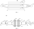
- FIG. 1 shows a schematic structural view of a conventional Mach-Zehnder modulator.
- the Mach-Zehnder modulator 001 has two waveguide arms 02 that are identical to each other.
- the Mach-Zehnder modulator 001 is not operating, neither of the two waveguide arms 02 undergoes an electro-optic effect.
- Input light passes through a light-splitting element 01 and is then equally split into two branch optical signals.
- the two branch optical signals are still in the same phase after respectively passing through one waveguide arm 02, and thus coherently enhanced signals of the two branch optical signals are output from a light-combining element 05.
- a modulation electrode 04 (for example, comprising a signal electrode 040, a first ground electrode 041 and a second ground electrode 042) applies a modulation voltage to the two waveguide arms 02, and the two branch optical signals may differ in phase by an odd or even multiple of II after each of the two branch optical signals passes through one waveguide arm 02.
- the light-combining element 05 outputs coherently enhanced signals of the two branch optical signals.
- the light-combining element 05 outputs coherent cancellation signals of the two branch optical signals.
- the two waveguide arms 02 cannot be identical absolutely due to reasons such as a material and electric charge accumulation; when the Mach-Zehnder modulator 001 is not operating, a certain phase deviation has appeared after the two branch optical signals respectively pass through one waveguide arm 02, this phase deviation is inevitable, is an inherent phase difference and may vary with changes in time and environmental conditions, and the existence of this phase deviation affects the accuracy of output signals when the Mach-Zehnder modulator 001 is operating, or even causes the Mach-Zehnder modulator 001 to be incapable of performing normal output.
- bias voltage modulation module to compensate the phase deviation caused by the inherent difference between the two waveguide arms, so as to improve the accuracy of operating signals output from the electro-optic modulator and thus improve the operating performance of the electro-optic modulator.
- the embodiments of the present disclosure provide an electro-optic modulator, in order to improve the accuracy of operating signals output from the electro-optic modulator.
- the electro-optic modulator 100 comprises a first light-splitting element 10, a second light-splitting element 20, two waveguide arms 70, a bias voltage modulation module 80, a radio frequency modulation module 90, a third light-splitting element 30 and a fourth light-splitting element 40.
- the first light-splitting element 10 comprises a first input port 101 configured to input an operating signal, a first output port 103 configured to output a main path signal, and a second output port 104 configured to output a first monitoring signal.
- the second light-splitting element 20 has a one-in two-out structure and an input port thereof being connected to the first output port 103, and is configured to equally split an optical signal input from the input port into two branch optical signals.
- the two waveguide arms 70 correspondingly provide transmission paths for the two branch optical signals, and one end of each of the waveguide arms is correspondingly connected to two output ports of the second light-splitting element 20.
- the third light-splitting element 30 has a two-in three-out structure and two input ports thereof being correspondingly connected to the other end of each of the two waveguide arms 70, and is configured to correspondingly receive the branch optical signals transmitted by means of the two waveguide arms 70.
- the fourth light-splitting element 40 has a one-in two-out structure and an input port thereof being connected to a first output port 301 of the third light-splitting element 30, and the fourth light-splitting element 40 comprises a third output port 401 configured to output a maximum optical power value and a fourth output port 402 configured to output a second monitoring signal.
- the radio frequency modulation module 90 is configured to apply a radio frequency voltage to the two waveguide arms 70 on the basis of a radio frequency signal to perform radio frequency modulation on the two branch optical signals transmitted therein, such that a phase difference is generated between the two branch optical signals.
- the bias voltage modulation module 80 is configured to apply a bias voltage to the two waveguide arms 70 on the basis of the bias voltage signal, to perform bias voltage modulation on the two branch optical signals transmitted therein.
- each light-splitting element refers to an optical power allocation element, for example, a multiple-mode interference element having an optical power allocation function.
- a designer can design actual structures of the light-splitting elements according to the designed allocation proportions of optical power.
- the operating signal input from the first input port 101 is normal, for example, whether the power for coupling the operating signal into the electro-optic modulator 100 can reach a target power.
- the second monitoring signal output from the fourth output port 402 of the fourth light-splitting element 40 and the signal output from the second output port 302 or the third output port 303 of the third light-splitting element 30 it can be monitored whether the operating state of the electro-optic modulator 100 is normal, for example, whether the two branch optical signals reach a target phase difference.
- FIG. 3 is a curve graph illustrating the correlation between the optical power output from the first output port 301 and the second output port 302 (which may also be the third output port 303) of the third light-splitting element 30 and the phase difference between the two branch optical signals.
- the optical power ratio K of the second monitoring signal (which is a set proportion of the optical power output from the first output port 301) output from the fourth output port 402 to the signal output from the second output port 302 or the third output port 303 of the third light-splitting element 30 reaches a maximum value, it can be obtained that the phase difference between the two branch optical signals is zero or an even multiple of II, and when the ratio K reaches a minimum value, it can be obtained that the phase difference between the two branch optical signals is an odd multiple of II.
- the operating signals and operating states input into the electro-optic modulator 100 can be monitored effectively; on the basis of these monitoring information, the bias voltage signal output to the bias voltage modulation module 80 is adjusted, and the phase deviation caused by the inherent difference between the two waveguide arms 70 can be compensated, so that the accuracy of the operating signals output from the electro-optic modulator 100 in the operating state can be improved.
- the encoding format of the electro-optic modulator 100 includes, but is not limited to, an NRZ encoding format and a PAM4 encoding format.
- the encoding formats of the electro-optic modulator 100 are different, and the specific settings of the target phase difference are also different.
- the electro-optic modulator 100 uses the NRZ (Non-return-to-zero Code) encoding format, so that the two branch optical signals can produce a first target phase difference ⁇ 1 and a second target phase difference ⁇ 2, and the first target phase difference ⁇ 1 and the second target phase difference ⁇ 2 satisfy:
- NRZ Non-return-to-zero Code
- the first target phase difference ⁇ 1 is represented by 2N ⁇
- the second target phase difference ⁇ 2 is represented by (2N + 1) ⁇
- the first target phase difference ⁇ 1 is represented by 2NII + 3 ⁇ /10
- the second target phase difference ⁇ 2 is represented by 2NII + 7 ⁇ /10
- the first target phase difference ⁇ 1 is represented by 2N ⁇ + ⁇ /10
- the second target phase difference ⁇ 2 is represented by 2NII + 9 ⁇ /10, and so on, which are not enumerated herein.
- a control chip of the electro-optic modulator 100 outputs a radio frequency modulation signal to the radio frequency modulation module 90 on the basis of the first target phase difference ⁇ 1 and the second target phase difference ⁇ 2.
- the electro-optic modulator 100 uses the PAM4 (4-Level Pulse Amplitude Modulation) encoding format, so that the two branch optical signals may produce the first target phase difference ⁇ 1, the second target phase difference ⁇ 2, the third target phase difference ⁇ 3, and the fourth target phase difference ⁇ 4.
- the first target phase difference ⁇ 1, the second target phase difference ⁇ 2, the third target phase difference ⁇ 3, and the fourth target phase difference ⁇ 4 satisfy:
- 3
- 3
- the control chip of the electro-optic modulator 100 outputs the radio frequency modulation signal to the radio frequency modulation module 90 on the basis of the first target phase difference ⁇ 1, the second target phase difference ⁇ 2, the third target phase difference ⁇ 3 and the fourth target phase difference ⁇ 4.
- the first output port 301 of the third light-splitting element 30 is configured to output the maximum optical power values of coherently enhanced signals (corresponding to the maximum energy values or maximum strength values of the coherently enhanced signals) of the two branch optical signals having the phase difference of 2N ⁇ , where N is 0 or a natural number; and the second output port 302 and the third output port 303 of the third light-splitting element 30 are configured to correspondingly output the set allocation proportions of the maximum optical power values of the coherently enhanced signals (corresponding to the maximum energy values or maximum strength values of the coherently enhanced signals) of the two branch optical signals having the phase difference of (2N + 1) ⁇ , wherein the set allocation proportions are greater than 0 and less than 1.
- the signals correspondingly output from the second output port 302 and the third output port 303 of the third light-splitting element 30 can both reach 50% of the maximum optical power values of the coherently enhanced signals of the two branch optical signals with a phase difference of (2N + 1) ⁇ .
- the signal output from the second output port 302 of the third light-splitting element 30 can reach 40% of the maximum optical power values of the coherently enhanced signals of the two branch optical signals with a phase difference of (2N + 1) ⁇ , and the signal output from the third output port 303 of the third light-splitting element 30 can reach 60% of the maximum optical power values of the coherently enhanced signals of the two branch optical signals with a phase difference of (2N + 1) ⁇ .
- a specific structural dimension of the third light-splitting element 30 can be designed on the basis of the set allocation proportions.
- the two branch optical signals When the phase difference between the two branch optical signals is (2N + 1) ⁇ , the two branch optical signals still produce coherent enhancement by utilizing the multiple-mode interference effect of the third light-splitting element 30, and the coherently enhanced signals are either equally divided or proportionally allocated between the second output port 302 and the third output port 303 of the third light-splitting element 30, output as monitoring signals and are capable of reaching the maximum optical power values thereof. Therefore, according to the technical solutions of the embodiments of the present disclosure, relatively strong monitoring signals can be obtained without substantially weakening the strength of the operating signals output from the electro-optic modulator 100, so that the effectiveness of monitoring is ensured.
- the third light-splitting element 30 has an axisymmetric structure, and the second output port 302 and the third output port 303 thereof are arranged symmetrically relative to the first output port 301.
- Such a design can allow the overall structure to be symmetrical and thus weaken the dependence of the element on the wavelength, so that the electro-optic modulator 100 is applicable to a wider signal waveband and has a larger application range.
- the electro-optic modulator 100 further comprises: a fifth light-splitting element 50, which has a one-in two-out structure and an input port thereof being connected to the second output port 302 of the third light-splitting element 30, the fifth light-splitting element comprising a fifth output port 501 configured to output a third monitoring signal and a sixth output port 502 configured to output a fourth monitoring signal; and a sixth light-splitting element 60, which has a one-in two-out structure and an input port thereof being connected to the third output port 303 of the third light-splitting element 30, the sixth light-splitting element comprising a seventh output port 601 configured to output a fifth monitoring signal and an eighth output port 602 configured to output a sixth monitoring signal.
- the structures of the fifth light-splitting element 50 and the sixth light-splitting element 60 may be identical completely. In addition, only one of the fifth light-splitting element 50 and the sixth light-splitting element
- the first input port 101 of the first light-splitting element 10 and the second input port 102 of the first light-splitting element 10 have exchange symmetry, and the first output port 103 and the second output port 104 have exchange symmetry; and/or, the third output port 401 of the fourth light-splitting element 40 and the fourth output port 402 of the fourth light-splitting element 40 have exchange symmetry; and/or, the fifth output port 501 of the fifth light-splitting element 50 and the sixth output port 502 of the fifth light-splitting element 50 have exchange symmetry; and/or, the seventh output port 601 of the sixth light-splitting element 60 and the eighth output port 602 of the sixth light-splitting element 60 have exchange symmetry.
- A% may be a constant value determined according to experience, or may be a constant value determined on the basis of the power ratio of the third monitoring signal to the fourth monitoring signal. In some embodiments of the present disclosure, A% mentioned above is less than 50%, for example, A% is valued as 3% or 5%.
- the first light-splitting element 10 further comprises a second input port 102 configured to input a detection signal.
- the second input port 102 can be used as a debugging and detection input port of the electro-optic modulator 100 at a product development or testing stage.
- the optical power input from the second input port 102 is represented by P0
- the maximum optical power value output from the third output port 401 is represented by P6
- A% is less than 50%, for example, A% is valued as 3% or 5%, which can allow most of the optical power to be output from the second output port 104, and is thus conductive to improving the detection accuracy.
- the transmission loss of the electro-optic modulator 100 using a certain design can be calculated. If the transmission loss is controlled within a target range, a product meets the ex-factory design requirements; and if the transmission loss is larger and not within the target range, the specific structural details of the product can be revised in design to reduce the transmission loss.
- the electro-optic modulator 100 further comprises a feedback module, which is configured to adjust the bias voltage signal output to the bias voltage modulation module 80 on the basis of at least one of the first monitoring signal, the second monitoring signal, the third monitoring signal, the fourth monitoring signal, the fifth monitoring signal, and the sixth monitoring signal.
- the feedback module may comprise a signal strength monitoring sensor located at a corresponding monitoring output port, and on the premise that an output operating signal of the electro-optic modulator 100 meets accuracy requirements, the signal strength monitoring sensor may detect a monitoring signal output from the output port in real time or at a certain frequency.
- the electro-optic modulator 100 itself has a function of monitoring the operating signals and the operating state, and can automatically and dynamically adjust the bias voltage signal output to the bias voltage modulation module 80 on the basis of these monitoring information, so as to compensate the phase deviation caused by the inherent difference between the two waveguide arms 70, so that the accuracy and reliability of the operating signals output from the electro-optic modulator 100 can be improved.
- the feedback module can also trigger an alarm unit of the electro-optic modulator 100 to give an alarm prompt.
- orientations or positional relationships or dimensions denoted by the terms such as “center”, “longitudinal”, “transverse”, “length”, “width”, “thickness”, “upper”, “lower”, “front”, “rear”, “left”, “right”, “vertical”, “horizontal”, “top”, “bottom”, “inner”, “outer”, “clockwise”, “counterclockwise”, “axial”, “radial” and “circumferential”, are the orientations or positional relationships or dimensions shown on the basis of the accompanying drawings, and these terms are used merely for ease of description, rather than indicating or implying that the device or element referred to must have particular orientations and be constructed and operated in the particular orientations, and therefore should not be construed as limiting the scope of protection of the present disclosure.
- first”, “second” and “third” are merely for descriptive purposes and should not be construed as indicating or implying relative importance or implicitly indicating the number of technical features indicated.
- the features defined with “first”, “second” and “third” may explicitly or implicitly include one or more features.
- the term “a plurality of” means two or more, unless otherwise explicitly and specifically defined.
- the terms such as “mounting”, “connection”, “connected” and “fixing” should be interpreted broadly, for example, they may be a fixed connection, a detachable connection, or an integrated connection; may be a mechanical connection, or an electrical connection, or communication; and may be a direct connection or an indirect connection by means of an intermediate medium, or may be internal communication between two elements or interaction between the two elements.
- the specific meanings of the above terms in the present disclosure can be understood according to specific circumstances.
- the expression of the first feature being “above” or “below” the second feature may include the case that the first feature is in direct contact with the second feature, or the case that the first feature and the second feature are not in direct contact but are contacted via another feature therebetween.
- the first feature being “over”, “above” or “on” the second feature includes the case that the first feature is directly or obliquely above the second feature, or merely indicates that the first feature is at a higher level than the second feature.
- the first feature being “below”, “under” or “beneath” the second feature includes the case that the first feature is directly or obliquely below the second feature, or merely indicates that the first feature is at a lower level than the second feature.
Landscapes
- Physics & Mathematics (AREA)
- Nonlinear Science (AREA)
- General Physics & Mathematics (AREA)
- Optics & Photonics (AREA)
- Electromagnetism (AREA)
- Chemical & Material Sciences (AREA)
- Engineering & Computer Science (AREA)
- Ceramic Engineering (AREA)
- Crystallography & Structural Chemistry (AREA)
- Optical Modulation, Optical Deflection, Nonlinear Optics, Optical Demodulation, Optical Logic Elements (AREA)
Applications Claiming Priority (2)
| Application Number | Priority Date | Filing Date | Title |
|---|---|---|---|
| CN202210177565.1A CN116699880A (zh) | 2022-02-25 | 2022-02-25 | 电光调制器 |
| PCT/CN2022/139311 WO2023160150A1 (zh) | 2022-02-25 | 2022-12-15 | 电光调制器 |
Publications (2)
| Publication Number | Publication Date |
|---|---|
| EP4459366A1 true EP4459366A1 (de) | 2024-11-06 |
| EP4459366A4 EP4459366A4 (de) | 2025-04-23 |
Family
ID=87764628
Family Applications (1)
| Application Number | Title | Priority Date | Filing Date |
|---|---|---|---|
| EP22928404.7A Pending EP4459366A4 (de) | 2022-02-25 | 2022-12-15 | Elektrooptischer modulator |
Country Status (5)
| Country | Link |
|---|---|
| US (1) | US20250216741A1 (de) |
| EP (1) | EP4459366A4 (de) |
| JP (1) | JP7836405B2 (de) |
| CN (1) | CN116699880A (de) |
| WO (1) | WO2023160150A1 (de) |
Family Cites Families (9)
| Publication number | Priority date | Publication date | Assignee | Title |
|---|---|---|---|---|
| JP4911529B2 (ja) * | 2005-02-22 | 2012-04-04 | 日本碍子株式会社 | 光変調器 |
| JP4874685B2 (ja) | 2005-03-25 | 2012-02-15 | 住友大阪セメント株式会社 | 光変調器 |
| US7508523B2 (en) | 2006-07-24 | 2009-03-24 | National Research Council Of Canada | Interferometric system for complex image extraction |
| JP4934557B2 (ja) | 2007-09-27 | 2012-05-16 | 株式会社日立製作所 | 4値位相変調器 |
| GB201020972D0 (en) * | 2010-12-10 | 2011-01-26 | Oclaro Technology Ltd | Assembly for monitoring output characteristics of a modulator |
| JP5660095B2 (ja) | 2012-08-31 | 2015-01-28 | 住友大阪セメント株式会社 | 光変調器 |
| KR102559579B1 (ko) | 2015-09-03 | 2023-07-25 | 삼성전자주식회사 | 광 변조기 및 이를 이용하는 데이터 처리 시스템 |
| US10901153B2 (en) * | 2018-12-24 | 2021-01-26 | Elenion Technologies, Llc | Null bias mach-zehnder interferometer with ring resonators |
| CN113176693A (zh) * | 2021-04-30 | 2021-07-27 | 南京刻得不错光电科技有限公司 | 多模干涉元件及马赫曾德尔调制器 |
-
2022
- 2022-02-25 CN CN202210177565.1A patent/CN116699880A/zh active Pending
- 2022-12-15 EP EP22928404.7A patent/EP4459366A4/de active Pending
- 2022-12-15 US US18/834,742 patent/US20250216741A1/en active Pending
- 2022-12-15 JP JP2024549721A patent/JP7836405B2/ja active Active
- 2022-12-15 WO PCT/CN2022/139311 patent/WO2023160150A1/zh not_active Ceased
Also Published As
| Publication number | Publication date |
|---|---|
| JP7836405B2 (ja) | 2026-03-26 |
| JP2025506794A (ja) | 2025-03-13 |
| WO2023160150A1 (zh) | 2023-08-31 |
| EP4459366A4 (de) | 2025-04-23 |
| US20250216741A1 (en) | 2025-07-03 |
| CN116699880A (zh) | 2023-09-05 |
Similar Documents
| Publication | Publication Date | Title |
|---|---|---|
| US12298610B2 (en) | Coplanar waveguide wire electrode structure and modulator | |
| US20250147379A1 (en) | Electro-optic modulator | |
| CN111458948B (zh) | 实现开关消光比提高的电光强度调制器及其应用 | |
| US20240235689A1 (en) | Optical signal sending apparatus | |
| CN115267360B (zh) | 一种基于晶体长度调制相位的电光型电场传感器 | |
| CN113467106A (zh) | 折叠型马赫曾德尔调制器 | |
| JP7796777B2 (ja) | 導波管線電極構造体および電気光学変調器 | |
| US20240192569A1 (en) | Electro-optic modulator | |
| EP4459366A1 (de) | Elektrooptischer modulator | |
| US20240361625A1 (en) | Folded electro-optic modulator | |
| US20250298284A1 (en) | Electro-optic modulator | |
| CN209657053U (zh) | 一种低压负啁啾调制器 | |
| US20240345423A1 (en) | Phase modulation module and electro-optic modulator | |
| JP2013122546A (ja) | 半導体光位相変調器及びその駆動方法 | |
| CN115004099A (zh) | 光信号复制装置 | |
| JP7796863B2 (ja) | 電気光学変調器および電気光学デバイス | |
| US20230065036A1 (en) | Optical device and optical communication apparatus | |
| CN118915335A (zh) | 高线性集成级联调制器 | |
| CN109856885A (zh) | 一种低压负啁啾调制器 | |
| US20250323731A1 (en) | Optical-mode modulation device and photonic chip | |
| GOTO et al. | Optical switching characteristics in slightly nondegenerated multilayered couplers using acousto-optic interaction by surface acoustic waves | |
| EP4006630A1 (de) | Verteilter lichtintensitätsmodulator | |
| CN115903284A (zh) | 电光调制器 | |
| JP3632714B2 (ja) | 電磁波受信システム | |
| CN120722496A (zh) | 一种片上偏振控制器及芯片 |
Legal Events
| Date | Code | Title | Description |
|---|---|---|---|
| STAA | Information on the status of an ep patent application or granted ep patent |
Free format text: STATUS: THE INTERNATIONAL PUBLICATION HAS BEEN MADE |
|
| PUAI | Public reference made under article 153(3) epc to a published international application that has entered the european phase |
Free format text: ORIGINAL CODE: 0009012 |
|
| STAA | Information on the status of an ep patent application or granted ep patent |
Free format text: STATUS: REQUEST FOR EXAMINATION WAS MADE |
|
| 17P | Request for examination filed |
Effective date: 20240729 |
|
| AK | Designated contracting states |
Kind code of ref document: A1 Designated state(s): AL AT BE BG CH CY CZ DE DK EE ES FI FR GB GR HR HU IE IS IT LI LT LU LV MC ME MK MT NL NO PL PT RO RS SE SI SK SM TR |
|
| A4 | Supplementary search report drawn up and despatched |
Effective date: 20250321 |
|
| RAP1 | Party data changed (applicant data changed or rights of an application transferred) |
Owner name: NANJING LYCORE TECHNOLOGIES CO., LTD. |
|
| RIC1 | Information provided on ipc code assigned before grant |
Ipc: G02F 1/035 20060101AFI20250317BHEP |
|
| DAV | Request for validation of the european patent (deleted) | ||
| DAX | Request for extension of the european patent (deleted) |