EP4459672A1 - Dispositifs de circuit intégré comprenant un espaceur intergrille et leurs procédés de fabrication - Google Patents
Dispositifs de circuit intégré comprenant un espaceur intergrille et leurs procédés de fabrication Download PDFInfo
- Publication number
- EP4459672A1 EP4459672A1 EP24166819.3A EP24166819A EP4459672A1 EP 4459672 A1 EP4459672 A1 EP 4459672A1 EP 24166819 A EP24166819 A EP 24166819A EP 4459672 A1 EP4459672 A1 EP 4459672A1
- Authority
- EP
- European Patent Office
- Prior art keywords
- spacer
- intergate
- channel region
- layer
- work function
- Prior art date
- Legal status (The legal status is an assumption and is not a legal conclusion. Google has not performed a legal analysis and makes no representation as to the accuracy of the status listed.)
- Pending
Links
Images


Classifications
-
- H—ELECTRICITY
- H10—SEMICONDUCTOR DEVICES; ELECTRIC SOLID-STATE DEVICES NOT OTHERWISE PROVIDED FOR
- H10D—INORGANIC ELECTRIC SEMICONDUCTOR DEVICES
- H10D84/00—Integrated devices formed in or on semiconductor substrates that comprise only semiconducting layers, e.g. on Si wafers or on GaAs-on-Si wafers
- H10D84/80—Integrated devices formed in or on semiconductor substrates that comprise only semiconducting layers, e.g. on Si wafers or on GaAs-on-Si wafers characterised by the integration of at least one component covered by groups H10D12/00 or H10D30/00, e.g. integration of IGFETs
- H10D84/82—Integrated devices formed in or on semiconductor substrates that comprise only semiconducting layers, e.g. on Si wafers or on GaAs-on-Si wafers characterised by the integration of at least one component covered by groups H10D12/00 or H10D30/00, e.g. integration of IGFETs of only field-effect components
- H10D84/83—Integrated devices formed in or on semiconductor substrates that comprise only semiconducting layers, e.g. on Si wafers or on GaAs-on-Si wafers characterised by the integration of at least one component covered by groups H10D12/00 or H10D30/00, e.g. integration of IGFETs of only field-effect components of only insulated-gate FETs [IGFET]
- H10D84/85—Complementary IGFETs, e.g. CMOS
- H10D84/856—Complementary IGFETs, e.g. CMOS the complementary IGFETs having different architectures than each other, e.g. high-voltage and low-voltage CMOS
-
- H—ELECTRICITY
- H10—SEMICONDUCTOR DEVICES; ELECTRIC SOLID-STATE DEVICES NOT OTHERWISE PROVIDED FOR
- H10D—INORGANIC ELECTRIC SEMICONDUCTOR DEVICES
- H10D30/00—Field-effect transistors [FET]
- H10D30/01—Manufacture or treatment
- H10D30/014—Manufacture or treatment of FETs having zero-dimensional [0D] or one-dimensional [1D] channels, e.g. quantum wire FETs, single-electron transistors [SET] or Coulomb blockade transistors
-
- H—ELECTRICITY
- H10—SEMICONDUCTOR DEVICES; ELECTRIC SOLID-STATE DEVICES NOT OTHERWISE PROVIDED FOR
- H10D—INORGANIC ELECTRIC SEMICONDUCTOR DEVICES
- H10D30/00—Field-effect transistors [FET]
- H10D30/40—FETs having zero-dimensional [0D], one-dimensional [1D] or two-dimensional [2D] charge carrier gas channels
- H10D30/43—FETs having zero-dimensional [0D], one-dimensional [1D] or two-dimensional [2D] charge carrier gas channels having one-dimensional [1D] charge carrier gas channels, e.g. quantum wire FETs or transistors having 1D quantum-confined channels
-
- H—ELECTRICITY
- H10—SEMICONDUCTOR DEVICES; ELECTRIC SOLID-STATE DEVICES NOT OTHERWISE PROVIDED FOR
- H10D—INORGANIC ELECTRIC SEMICONDUCTOR DEVICES
- H10D30/00—Field-effect transistors [FET]
- H10D30/60—Insulated-gate field-effect transistors [IGFET]
- H10D30/67—Thin-film transistors [TFT]
- H10D30/6729—Thin-film transistors [TFT] characterised by the electrodes
- H10D30/673—Thin-film transistors [TFT] characterised by the electrodes characterised by the shapes, relative sizes or dispositions of the gate electrodes
- H10D30/6735—Thin-film transistors [TFT] characterised by the electrodes characterised by the shapes, relative sizes or dispositions of the gate electrodes having gates fully surrounding the channels, e.g. gate-all-around
-
- H—ELECTRICITY
- H10—SEMICONDUCTOR DEVICES; ELECTRIC SOLID-STATE DEVICES NOT OTHERWISE PROVIDED FOR
- H10D—INORGANIC ELECTRIC SEMICONDUCTOR DEVICES
- H10D30/00—Field-effect transistors [FET]
- H10D30/60—Insulated-gate field-effect transistors [IGFET]
- H10D30/67—Thin-film transistors [TFT]
- H10D30/6757—Thin-film transistors [TFT] characterised by the structure of the channel, e.g. transverse or longitudinal shape or doping profile
-
- H—ELECTRICITY
- H10—SEMICONDUCTOR DEVICES; ELECTRIC SOLID-STATE DEVICES NOT OTHERWISE PROVIDED FOR
- H10D—INORGANIC ELECTRIC SEMICONDUCTOR DEVICES
- H10D62/00—Semiconductor bodies, or regions thereof, of devices having potential barriers
- H10D62/10—Shapes, relative sizes or dispositions of the regions of the semiconductor bodies; Shapes of the semiconductor bodies
- H10D62/113—Isolations within a component, i.e. internal isolations
- H10D62/115—Dielectric isolations, e.g. air gaps
-
- H—ELECTRICITY
- H10—SEMICONDUCTOR DEVICES; ELECTRIC SOLID-STATE DEVICES NOT OTHERWISE PROVIDED FOR
- H10D—INORGANIC ELECTRIC SEMICONDUCTOR DEVICES
- H10D62/00—Semiconductor bodies, or regions thereof, of devices having potential barriers
- H10D62/10—Shapes, relative sizes or dispositions of the regions of the semiconductor bodies; Shapes of the semiconductor bodies
- H10D62/117—Shapes of semiconductor bodies
- H10D62/118—Nanostructure semiconductor bodies
- H10D62/119—Nanowire, nanosheet or nanotube semiconductor bodies
- H10D62/121—Nanowire, nanosheet or nanotube semiconductor bodies oriented parallel to substrates
-
- H—ELECTRICITY
- H10—SEMICONDUCTOR DEVICES; ELECTRIC SOLID-STATE DEVICES NOT OTHERWISE PROVIDED FOR
- H10D—INORGANIC ELECTRIC SEMICONDUCTOR DEVICES
- H10D64/00—Electrodes of devices having potential barriers
- H10D64/01—Manufacture or treatment
- H10D64/017—Manufacture or treatment using dummy gates in processes wherein at least parts of the final gates are self-aligned to the dummy gates, i.e. replacement gate processes
-
- H—ELECTRICITY
- H10—SEMICONDUCTOR DEVICES; ELECTRIC SOLID-STATE DEVICES NOT OTHERWISE PROVIDED FOR
- H10D—INORGANIC ELECTRIC SEMICONDUCTOR DEVICES
- H10D84/00—Integrated devices formed in or on semiconductor substrates that comprise only semiconducting layers, e.g. on Si wafers or on GaAs-on-Si wafers
- H10D84/01—Manufacture or treatment
- H10D84/0123—Integrating together multiple components covered by H10D12/00 or H10D30/00, e.g. integrating multiple IGBTs
- H10D84/0126—Integrating together multiple components covered by H10D12/00 or H10D30/00, e.g. integrating multiple IGBTs the components including insulated gates, e.g. IGFETs
- H10D84/0165—Integrating together multiple components covered by H10D12/00 or H10D30/00, e.g. integrating multiple IGBTs the components including insulated gates, e.g. IGFETs the components including complementary IGFETs, e.g. CMOS devices
- H10D84/0167—Manufacturing their channels
-
- H—ELECTRICITY
- H10—SEMICONDUCTOR DEVICES; ELECTRIC SOLID-STATE DEVICES NOT OTHERWISE PROVIDED FOR
- H10D—INORGANIC ELECTRIC SEMICONDUCTOR DEVICES
- H10D84/00—Integrated devices formed in or on semiconductor substrates that comprise only semiconducting layers, e.g. on Si wafers or on GaAs-on-Si wafers
- H10D84/01—Manufacture or treatment
- H10D84/0123—Integrating together multiple components covered by H10D12/00 or H10D30/00, e.g. integrating multiple IGBTs
- H10D84/0126—Integrating together multiple components covered by H10D12/00 or H10D30/00, e.g. integrating multiple IGBTs the components including insulated gates, e.g. IGFETs
- H10D84/0165—Integrating together multiple components covered by H10D12/00 or H10D30/00, e.g. integrating multiple IGBTs the components including insulated gates, e.g. IGFETs the components including complementary IGFETs, e.g. CMOS devices
- H10D84/0172—Manufacturing their gate conductors
- H10D84/0177—Manufacturing their gate conductors the gate conductors having different materials or different implants
-
- H—ELECTRICITY
- H10—SEMICONDUCTOR DEVICES; ELECTRIC SOLID-STATE DEVICES NOT OTHERWISE PROVIDED FOR
- H10D—INORGANIC ELECTRIC SEMICONDUCTOR DEVICES
- H10D84/00—Integrated devices formed in or on semiconductor substrates that comprise only semiconducting layers, e.g. on Si wafers or on GaAs-on-Si wafers
- H10D84/01—Manufacture or treatment
- H10D84/0123—Integrating together multiple components covered by H10D12/00 or H10D30/00, e.g. integrating multiple IGBTs
- H10D84/0126—Integrating together multiple components covered by H10D12/00 or H10D30/00, e.g. integrating multiple IGBTs the components including insulated gates, e.g. IGFETs
- H10D84/0165—Integrating together multiple components covered by H10D12/00 or H10D30/00, e.g. integrating multiple IGBTs the components including insulated gates, e.g. IGFETs the components including complementary IGFETs, e.g. CMOS devices
- H10D84/0184—Manufacturing their gate sidewall spacers
-
- H—ELECTRICITY
- H10—SEMICONDUCTOR DEVICES; ELECTRIC SOLID-STATE DEVICES NOT OTHERWISE PROVIDED FOR
- H10D—INORGANIC ELECTRIC SEMICONDUCTOR DEVICES
- H10D84/00—Integrated devices formed in or on semiconductor substrates that comprise only semiconducting layers, e.g. on Si wafers or on GaAs-on-Si wafers
- H10D84/01—Manufacture or treatment
- H10D84/0123—Integrating together multiple components covered by H10D12/00 or H10D30/00, e.g. integrating multiple IGBTs
- H10D84/0126—Integrating together multiple components covered by H10D12/00 or H10D30/00, e.g. integrating multiple IGBTs the components including insulated gates, e.g. IGFETs
- H10D84/0165—Integrating together multiple components covered by H10D12/00 or H10D30/00, e.g. integrating multiple IGBTs the components including insulated gates, e.g. IGFETs the components including complementary IGFETs, e.g. CMOS devices
- H10D84/0193—Integrating together multiple components covered by H10D12/00 or H10D30/00, e.g. integrating multiple IGBTs the components including insulated gates, e.g. IGFETs the components including complementary IGFETs, e.g. CMOS devices the components including FinFETs
-
- H—ELECTRICITY
- H10—SEMICONDUCTOR DEVICES; ELECTRIC SOLID-STATE DEVICES NOT OTHERWISE PROVIDED FOR
- H10D—INORGANIC ELECTRIC SEMICONDUCTOR DEVICES
- H10D84/00—Integrated devices formed in or on semiconductor substrates that comprise only semiconducting layers, e.g. on Si wafers or on GaAs-on-Si wafers
- H10D84/80—Integrated devices formed in or on semiconductor substrates that comprise only semiconducting layers, e.g. on Si wafers or on GaAs-on-Si wafers characterised by the integration of at least one component covered by groups H10D12/00 or H10D30/00, e.g. integration of IGFETs
- H10D84/82—Integrated devices formed in or on semiconductor substrates that comprise only semiconducting layers, e.g. on Si wafers or on GaAs-on-Si wafers characterised by the integration of at least one component covered by groups H10D12/00 or H10D30/00, e.g. integration of IGFETs of only field-effect components
- H10D84/83—Integrated devices formed in or on semiconductor substrates that comprise only semiconducting layers, e.g. on Si wafers or on GaAs-on-Si wafers characterised by the integration of at least one component covered by groups H10D12/00 or H10D30/00, e.g. integration of IGFETs of only field-effect components of only insulated-gate FETs [IGFET]
- H10D84/85—Complementary IGFETs, e.g. CMOS
-
- H—ELECTRICITY
- H10—SEMICONDUCTOR DEVICES; ELECTRIC SOLID-STATE DEVICES NOT OTHERWISE PROVIDED FOR
- H10D—INORGANIC ELECTRIC SEMICONDUCTOR DEVICES
- H10D86/00—Integrated devices formed in or on insulating or conducting substrates, e.g. formed in silicon-on-insulator [SOI] substrates or on stainless steel or glass substrates
- H10D86/01—Manufacture or treatment
-
- H—ELECTRICITY
- H10—SEMICONDUCTOR DEVICES; ELECTRIC SOLID-STATE DEVICES NOT OTHERWISE PROVIDED FOR
- H10D—INORGANIC ELECTRIC SEMICONDUCTOR DEVICES
- H10D86/00—Integrated devices formed in or on insulating or conducting substrates, e.g. formed in silicon-on-insulator [SOI] substrates or on stainless steel or glass substrates
- H10D86/201—Integrated devices formed in or on insulating or conducting substrates, e.g. formed in silicon-on-insulator [SOI] substrates or on stainless steel or glass substrates the substrates comprising an insulating layer on a semiconductor body, e.g. SOI
-
- H—ELECTRICITY
- H10—SEMICONDUCTOR DEVICES; ELECTRIC SOLID-STATE DEVICES NOT OTHERWISE PROVIDED FOR
- H10D—INORGANIC ELECTRIC SEMICONDUCTOR DEVICES
- H10D88/00—Three-dimensional [3D] integrated devices
-
- B—PERFORMING OPERATIONS; TRANSPORTING
- B82—NANOTECHNOLOGY
- B82Y—SPECIFIC USES OR APPLICATIONS OF NANOSTRUCTURES; MEASUREMENT OR ANALYSIS OF NANOSTRUCTURES; MANUFACTURE OR TREATMENT OF NANOSTRUCTURES
- B82Y10/00—Nanotechnology for information processing, storage or transmission, e.g. quantum computing or single electron logic
-
- H—ELECTRICITY
- H10—SEMICONDUCTOR DEVICES; ELECTRIC SOLID-STATE DEVICES NOT OTHERWISE PROVIDED FOR
- H10D—INORGANIC ELECTRIC SEMICONDUCTOR DEVICES
- H10D84/00—Integrated devices formed in or on semiconductor substrates that comprise only semiconducting layers, e.g. on Si wafers or on GaAs-on-Si wafers
- H10D84/01—Manufacture or treatment
- H10D84/0123—Integrating together multiple components covered by H10D12/00 or H10D30/00, e.g. integrating multiple IGBTs
- H10D84/0126—Integrating together multiple components covered by H10D12/00 or H10D30/00, e.g. integrating multiple IGBTs the components including insulated gates, e.g. IGFETs
- H10D84/0165—Integrating together multiple components covered by H10D12/00 or H10D30/00, e.g. integrating multiple IGBTs the components including insulated gates, e.g. IGFETs the components including complementary IGFETs, e.g. CMOS devices
- H10D84/0172—Manufacturing their gate conductors
- H10D84/0179—Manufacturing their gate conductors the gate conductors having different shapes or dimensions
-
- H—ELECTRICITY
- H10—SEMICONDUCTOR DEVICES; ELECTRIC SOLID-STATE DEVICES NOT OTHERWISE PROVIDED FOR
- H10D—INORGANIC ELECTRIC SEMICONDUCTOR DEVICES
- H10D84/00—Integrated devices formed in or on semiconductor substrates that comprise only semiconducting layers, e.g. on Si wafers or on GaAs-on-Si wafers
- H10D84/01—Manufacture or treatment
- H10D84/02—Manufacture or treatment characterised by using material-based technologies
- H10D84/03—Manufacture or treatment characterised by using material-based technologies using Group IV technology, e.g. silicon technology or silicon-carbide [SiC] technology
- H10D84/038—Manufacture or treatment characterised by using material-based technologies using Group IV technology, e.g. silicon technology or silicon-carbide [SiC] technology using silicon technology, e.g. SiGe
-
- H—ELECTRICITY
- H10—SEMICONDUCTOR DEVICES; ELECTRIC SOLID-STATE DEVICES NOT OTHERWISE PROVIDED FOR
- H10D—INORGANIC ELECTRIC SEMICONDUCTOR DEVICES
- H10D88/00—Three-dimensional [3D] integrated devices
- H10D88/01—Manufacture or treatment
Definitions
- the present disclosure generally relates to the field of integrated circuit devices and, more particularly, to integrated circuit devices including stacked transistors.
- An integrated circuit device comprising: an upper transistor on a substrate, the upper transistor comprising an upper channel region; a lower transistor between the substrate and the upper transistor, the lower transistor comprising a lower channel region; an intergate spacer comprising an insulating material and adjacent to a side surface of the lower channel region; and a gate layer, wherein the intergate spacer is between the side surface of the lower channel region and the gate layer.
- An integrated circuit device comprising: an upper transistor on a substrate, the upper transistor comprising an upper channel region; a lower transistor between the substrate and the upper transistor, the lower transistor comprising a lower channel region and a lower work function layer on the lower channel region; an intergate spacer comprising an insulating material, wherein the lower work function layer is between the lower channel region and the intergate spacer; and a gate layer on the intergate spacer.
- a method of forming an integrated circuit device comprising: forming a lower stack and an upper stack on a substrate, wherein the lower stack is between the substrate and the upper stack, the lower stack comprises a lower sacrificial pattern and a lower channel region stacked in a vertical direction, and the upper stack comprises an upper sacrificial pattern and an upper channel region stacked in the vertical direction; forming a dummy gate insulator on the lower stack and the upper stack; forming an intergate spacer adjacent to a side surface of the lower stack; removing the dummy gate insulator, the lower sacrificial pattern and the upper sacrificial pattern, thereby exposing the lower channel region and the upper channel region and forming a cavity between the lower channel region and the intergate spacer; forming a gate insulator on the lower channel region and the upper channel region; forming a lower work function layer on the gate insulator and in the cavity between the lower channel region and the intergate spacer; forming an upper work function layer on the lower work function
- an integrated circuit device may include a stacked transistor structure including a lower transistor on a substrate and an upper transistor vertically stacked on the lower transistor.
- the upper transistor may include a plurality of upper channel regions
- the lower transistor may include a plurality of lower channel regions.
- Processes of forming a lower work function layer between the lower channel regions may include forming a preliminary work function layer on the lower channel regions and the upper channel regions and removing an upper portion of the preliminary work function layer formed on the upper channel regions. The remaining lower portion of the preliminary work function layer on the lower channel regions may be the lower work function layer. While removing the upper portion of the preliminary work function layer formed on the upper channel regions, the preliminary work function layer between the lower channel regions may be partially and inwardly etched and form recessed or pinched-off regions. During the subsequent upper work function layer formation process, the recessed or pinched-off regions may be deposited by the upper work function layer so that the performance of the lower transistor may be degraded. To improve the performance of the lower transistor, the recessed or pinched-off regions should be reduced.
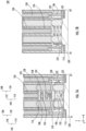
- FIG. 1 is a plan view of an integrated circuit device 100 according to some embodiments.
- FIG. 1A is a cross-sectional view of the integrated circuit device 100 taken along line X1-X1' in FIG. 1 according to some embodiments.
- FIG. 1B is a cross-sectional view of the integrated circuit device 100 taken along line X2-X2' in FIG. 1 according to some embodiments.
- FIG. 1C is a cross-sectional view of the integrated circuit device 100 taken along line Y1-Y1' in FIG. 1 according to some embodiments.
- FIG. 1D is a cross-sectional view of the integrated circuit device 100 taken along line Y2-Y2' in FIG. 1 according to some embodiments. Referring to FIGS.
- the integrated circuit device 100 may include a substrate 120, a lower transistor 102 on the substrate 120, an upper transistor 104 on the lower transistor 102.
- the lower transistor 102 may be between the substrate 120 and the upper transistor 104.
- the lower transistor 102 may include a lower channel region 106.
- the upper transistor 104 may include an upper channel region 108.
- the upper and lower channel regions 108 and 106 may include, for example, a semiconductor material such as silicon (Si).
- Si silicon
- the integrated circuit device 100 may include multiple upper transistors and lower transistors.
- the integrated circuit device 100 may further include an integrated insulator 118 between the lower transistor 102 and the upper transistor 104 (e.g., between the lower channel region 106 and the upper channel region 108) in a Z-direction (also referred to a vertical direction or a third direction).
- the integrated insulator e.g., the integrated insulator 118
- the integrated insulator 118 may be also referred to as an intergate insulator.
- the integrated insulator 118 may include multiple layers.
- the integrated insulator 118 may include silicon nitride (SiN), siliconboron carbonitride (SiBCN), and/or silicon oxycarbonitride (SiOCN), but is not limited thereto.
- the substrate 120 may include an upper surface facing the lower channel region 106, and the Z-direction may be perpendicular to the upper surface of the substrate 120.
- the upper channel region 108 may include a plurality of upper channel regions 108 stacked in the Z-direction.
- the upper channel regions 108 may be spaced apart from each other in the Z-direction.
- the upper transistor 104 may further include an upper source/drain region 116 that is electrically connected to and/or is in contact with the upper channel regions 108.
- the upper channel regions 108 may be disposed between a pair of the upper source/drain regions 116 that are spaced apart from each other in a X-direction (also referred to as a first horizontal direction or a first direction).
- the X-direction may be parallel to the upper surface of the substrate 120 and may be perpendicular to the Z-direction.
- the lower channel region 106 may include a plurality of lower channel regions 106 stacked in the Z-direction.
- the lower channel regions 106 may be spaced apart from each other in the Z-direction.
- the lower transistor 102 may further include a lower source/drain region 114 that is electrically connected to and/or is in contact with the lower channel regions 106.
- the lower channel regions 106 may be disposed between a pair of the lower source/drain regions 114 that are spaced apart from each other in the X-direction.
- Each of the upper channel region 108 and the lower channel region 106 may include, for example, semiconductor material(s) (e.g., Si, Ge, SiGe, GaP, GaAs, SiC, SiGeC, and/or InP).
- Each of the upper channel regions 108 and the lower channel regions 106 may be, for example, a nanosheet that may have a thickness in a range of from 1 nm to 100 nm in the Z-direction or may be a nanowire that may have a circular cross-section with a diameter in a range of from 1 nm to 100 nm.
- the thicknesses or the diameters of the upper channel regions 108 and the lower channel regions 106 may not limit the present inventive concept.
- the upper source/drain region 116 may include a different semiconductor material from that of the lower source/drain region 114.
- the upper source/drain region 116 may include silicon germanium (SiGe), and the lower source/drain region 114 may include silicon (Si).
- the upper transistor 104 may further include an upper gate structure 112 on the upper channel regions 108.
- the upper gate structure 112 may include a portion of a gate layer 128 (e.g., an upper portion of the gate layer 128) and an upper work function layer 124. Further, the upper gate structure 112 may include an upper gate insulator that extends between the upper channel region 108 and the upper work function layer 124 to separate the upper channel region 108 and the upper work function layer 124 from each other.
- the upper work function layer 124 may be disposed on the upper channel region 108.
- a portion of the upper work function layer 124 may be disposed in a space between two adjacent upper channel regions 108.
- a portion of the gate layer 128 e.g., an upper portion of the gate layer 128, may be disposed in the space between two adjacent upper channel regions 108.
- the portion of the upper work function layer 124 may extend around the portion of the gate layer 128 (e.g., an upper portion of the gate layer 128) in the space between two adj acent upper channel regions 108.
- the lower transistor 102 may further include a lower gate structure 110 on the lower channel regions 106.
- the lower gate structure 110 may include a portion of the gate layer 128 (e.g., a lower portion of the gate layer 128) and a lower work function layer 122. Further, the lower gate structure 110 may include a lower gate insulator that extends between the lower channel region 106 and the lower work function layer 122 to separate the lower channel region 106 and the lower work function layer 122 from each other.
- the lower work function layer 122 may be disposed on the lower channel region 106.
- a portion of the lower work function layer 122 may be disposed in a space between two adjacent lower channel regions 106.
- a portion of the gate layer 128 (e.g., a lower portion of the gate layer 128) may be disposed in the space between two adjacent lower channel regions 106.
- the portion of the lower work function layer 122 may extend around the portion of the gate layer 128 (e.g., a lower portion of the gate layer 128) in the space between two adjacent lower channel regions 106.
- the embodiments of the present inventive concept are not limited thereto.
- the lower work function layer 122 may fill the space between two adjacent lower channel regions 106 without the gate layer 128 (e.g., without a lower portion of the gate layer 128).
- the gate layer 128 (e.g., each of the upper and lower portions of the gate layer 128) may include, for example, tungsten (W), aluminum (Al) and/or copper (Cu).
- the upper and lower portions of the gate layer 128 may comprise an integrated unitary structure.
- the upper and lower portions of the gate layer 128 may comprise an upper gate layer (referring to upper gate layer 1728b in FIGS. 17A and 17B ) and a lower gate layer (referring to lower gate layer 1728a in FIGS. 17A and 17B ), respectively.
- the upper transistor 104 and the lower transistor 102 may have different conductivity types.
- the upper transistor 104 may be a p-type transistor, and the upper work function layer 124 may include a p-type work function layer (e.g., TiN layer).
- the lower transistor 102 may be an n-type transistor, and the lower work function layer 122 may include an n-type work function layer (e.g., TiC layer, TiAl layer and/or TiAlC layer).
- Each of the lower work function layer 122 and the upper work function layer 124 may be a single layer or may include multiple layers.
- the integrated insulator 118 may be disposed between the upper work function layer 124 and the lower work function layer 122.
- two adjacent lower channel regions 106 may be spaced apart from each other by a first distance D1 in the vertical direction.
- two adjacent upper channel regions 108 may be spaced apart from each other by a second distance D2 in the vertical direction.
- the second distance D2 may be longer than the first distance D1.
- the first distance D1 may be in a range of from 3 nanometers (nm) to 12 nm (e.g., about 8 nm)
- the second distance D2 may be in a range of from 10 nm to 20 nm (e.g., about 15 nm).
- the integrated circuit device 100 may further include an intergate spacer 130 adjacent to the lower transistor 102.
- the intergate spacer 130 may be adjacent to a side surface of the lower channel region 106.
- the intergate spacer 130 may be spaced apart from a side surface of the lower channel region 106 by a third distance D3 in the X-direction and/or Y-direction (also referred to as a second horizontal direction or a second direction).
- the Y-direction may be parallel to the upper surface of the substrate 120 and may be perpendicular to the X-direction and/or the Z-direction.
- the third distance D3 may be equal to or longer than the first distance D1.
- the intergate spacer 130 may be disposed (e.g., may extend) between a side surface of the lower channel region 106 and the lower gate structure 110 (e.g., a lower portion of the gate layer 128 and/or lower work function layer 122).
- the intergate spacer 130 may be disposed (e.g., may extend) between the side surface of the lower channel region 106 and the lower work function layer 122.
- the intergate spacer 130 may be disposed between the side surface of the lower channel region 106 and the gate layer 128 (e.g., a lower portion of the gate layer 128, referring to lower gate layer 1728a in FIGS. 17A and 17B ).
- the gate layer 128 (e.g., a lower portion of the gate layer 128, referring to lower gate layer 1728a in FIGS. 17A and 17B ) may be disposed on the intergate spacer 130.
- the intergate spacer 130 may extend between the lower work function layer 122 and the gate layer 128 (e.g., a lower portion of the gate layer 128, referring to lower gate layer 1728a in FIGS. 17A and 17B ).
- opposing side surfaces of the intergate spacer 130 may be in contact with the lower work function layer 122 and the gate layer 128 (e.g., a lower portion of the gate layer 128, referring to lower gate layer 1728a in FIGS. 17A and 17B ), respectively.
- the lower work function layer 122 may be in contact with the lower channel region 106 and the intergate spacer 130.
- a lower surface of the upper channel region 108 may be closer than an upper surface of the intergate spacer 130 to the substrate 120 in the Z-direction.
- the intergate spacer 130 may comprise opposing side surfaces that contact the lower work function layer 122 and the upper work function layer 124, respectively.
- the intergate spacer 130 may be a single layer or may comprise multiple layers (referring to a first sub-intergate spacer 1830a and a second sub-intergate spacer 1830b in FIGS. 18A and 18B ) having different materials.
- the intergate spacer 130 may include, for example, an insulating material, such as silicon nitride (e.g., SiN), and/or a semiconductor material, such as poly-silicon.
- the upper transistor 104 may further include an upper inner spacer layer 134.
- the upper inner spacer layer 134 may be disposed between the upper source/drain region 116 and the upper gate structure 112, which are spaced apart from each other in the X-direction.
- the upper inner spacer layer 134 may be disposed between the upper channel regions 108, which are spaced apart from each other in the Z-direction.
- the lower transistor 102 may further include a lower inner spacer layer 132.
- the lower inner spacer layer 132 may be disposed between the lower source/drain region 114 and the lower gate structure 110, which are spaced apart from each other in the X-direction.
- the lower inner spacer layer 132 may be disposed between the lower channel regions 106, which are spaced apart from each other in the Z-direction.
- a side surface of the upper inner spacer layer 134 may be in contact with the upper source/drain region 116.
- a side surface of the lower inner spacer layer 132 may be in contact with the lower source/drain region 114.
- the upper inner spacer layer 134 may include, for example, silicon nitride (SiN).
- the upper inner spacer layer 134 (e.g., a lower surface of the upper inner spacer layer 134) may be in contact with the integrated insulator 118 (e.g., an upper surface of the integrated insulator 118).
- the lower inner spacer layer 132 may include, for example, silicon nitride (SiN).
- the lower inner spacer layer 132 (e.g., an upper surface of the lower inner spacer layer 132) may be in contact with the integrated insulator 118 (e.g., a lower surface of the integrated insulator 118).
- the integrated circuit device 100 may further include a gate spacer 126 on a side surface of the upper gate structure 112 of the upper transistor 104.
- the gate spacer 126 may be on a side surface of the upper work function layer 124.
- the gate spacer 126 may be on a side surface of the upper portion of the gate layer 128 (e.g., referring to an upper gate layer 1728b in FIGS. 17A and 17B ).
- the gate spacer 126 may be in contact with the upper gate structure 112.
- the gate spacer 126 may be in contact with a side surface of the upper work function layer 124.
- the gate spacer 126 may include, for example, SiBCN and/or SiOCN.
- the gate spacer 126 may be on a side surface of the lower gate structure 110 of the lower transistor 102.
- the gate spacer 126 may be on a side surface of the lower work function layer 122.
- the gate spacer 126 may be on a side surface of the lower portion of the gate layer 128 (e.g., referring to a lower gate layer 1728a in FIGS. 17A and 17B ).
- the gate spacer 126 may be in contact with the lower gate structure 110.
- the gate spacer 126 may be in contact with a side surface of the lower work function layer 122 and/or lower portion of the gate layer 128.
- the size of the upper channel region 108 may be smaller than that of the lower channel region 106.
- the length of the upper channel region 108 in the Y-direction may be shorter than the length of the lower channel region 106 in the Y-direction.
- the length of the upper channel region 108 in the X-direction may be the same as the length of the lower channel region 106 in the X-direction.
- the upper channel region 108 and the lower channel region 106 may comprise an L-shape.
- a first portion of the intergate spacer 130 and a second portion of the intergate spacer 130 may be spaced apart from each other in the Y-direction.
- the first portion of the intergate spacer 130 may be closer to the upper channel region 108 in the Y-direction.
- the second portion of the intergate spacer 130 may be farther from the upper channel region 108 in the Y-direction.
- the first portion of the intergate spacer 130 may have a flat or substantially flat upper surface.
- the second portion of the intergate spacer 130 may have, for example, a curved or rounded upper surface.
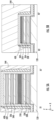
- FIG. 2 is a plan view of an integrated circuit device 200 according to some embodiments.
- FIG. 2A is a cross-sectional view of the integrated circuit device 200 taken along line X1-X1' in FIG. 2 according to some embodiments.
- FIG. 2B is a cross-sectional view of the integrated circuit device 200 taken along line Y1-Y1' in FIG. 2 according to some embodiments.
- the size of the upper channel region 208 may be the same size of the lower channel region 106.
- the lengths of the upper channel region 208 in the X-direction and Y-direction may be the same as those of the lower channel region 106, respectively.
- the upper channel region 208 and the lower channel region 106 may comprise an I-shape.
- a first portion of the intergate spacer 130 and a second portion of the intergate spacer 130 may be spaced apart from each other in the Y-direction.
- Each of the first and second portions of the intergate spacer 130 may have a flat or substantially flat upper surface.
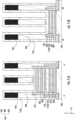
- FIGS. 3A, 3B , 3C , and 3D through 16A , 16B , 16C, and 16D are cross-sectional views illustrating methods of forming the integrated circuit device 100 in FIGS. 1 , 1A , 1B , 1C, and 1D according to some embodiments.
- the methods of manufacturing the integrated circuit device 100 may include forming a preliminary stack structure 332 on a substrate 120.
- the preliminary stack structure 332 may include a lower stack including a lower channel layer 334 on the substrate 120 and an upper stack including an upper channel layer 336 on the lower stack.
- the lower channel layer 334 may include a plurality of lower channel layers 334.
- the upper channel layer 336 may include a plurality of upper channel layers 336.
- the lower stack of the preliminary stack structure 332 may also include a plurality of lower sacrificial layers 338 formed on the substrate 120, and the upper stack of the preliminary stack structure 332 may include a plurality of upper sacrificial layers 340 formed on the plurality of lower sacrificial layers 338.
- the lower sacrificial layers 338 may be alternately stacked with the lower channel layers 334 in the lower stack.
- the upper sacrificial layers 340 may be alternately stacked with the upper channel layers 336 in the upper stack.
- the upper sacrificial layers 340 and the lower sacrificial layers 338 may be selectively removed with respect to the lower and upper channel layers 334 and 336 and thus may include material(s) different from the lower and upper channel layers 334 and 336.
- the upper and lower sacrificial layers 340 and 338 may include, for example, silicon germanium (SiGe).
- An integrated sacrificial layer 318 may be formed between the lower sacrificial layers 338 and the upper sacrificial layers 340.
- the integrated sacrificial layer 318 may have a larger thickness than each of the lower and upper channel layers 334 and 336, and each of the lower and upper sacrificial layers 338 and 340 in the Z-direction.
- the lower channel layers 334, the upper channel layers 336, and the integrated sacrificial layer 318 may be semiconductor layers that include, for example, silicon (Si).
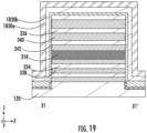
- a dummy gate insulator 342 and a preliminary intergate spacer layer 330 may be formed sequentially on the preliminary stack structure 332.
- the preliminary intergate spacer layer 330 may be formed on (e.g., may cover) an upper surface and side surfaces of the dummy gate insulator 342.
- the dummy gate insulator 342 may include oxide (e.g., SiO 2 ), and the preliminary intergate spacer layer 330 may include nitride (e.g., SiN).
- each of the dummy gate insulator 342 and the preliminary intergate spacer layer 330 may have a uniform thickness.
- the dummy gate insulator 342 may conformally extend along the upper surface and the side surfaces of the preliminary stack structure 332, and the preliminary intergate spacer layer 330 may conformally extend along the upper surface and the side surfaces of the dummy gate insulator 342, as illustrated in FIG. 3A .
- FIG. 3A illustrates the dummy gate insulator 342 as a single layer
- the dummy gate insulator 342 may include multiple layers sequentially stacked on the preliminary stack structure 332.
- the dummy gate insulator 342 may include a semiconductor layer (e.g., a polysilicon layer) and an insulating layer (e.g., a silicon oxide layer) sequentially stacked on the preliminary stack structure 332.
- the semiconductor layer of the dummy gate insulator 342 may extend between the preliminary stack structure 332 and the insulating layer of the dummy gate insulator 342.
- the semiconductor layer of the dummy gate insulator 342 may have a thickness thicker than a thickness of the insulating layer of the dummy gate insulator 342.
- the thickness of the semiconductor layer of the dummy gate insulator 342 may be in a range of from 2 nanometers (nm) to 10 nm (e.g., about 5.5 nm), and the thickness of the insulating layer of the dummy gate insulator 342 may be in a range of from 1 nm to 5 nm (e.g., about 2.5 nm).
- an upper portion of the preliminary intergate spacer layer 330 may be removed to form a preliminary intergate spacer 430.
- the preliminary intergate spacer 430 may expose an upper surface of the dummy gate insulator 342.
- the preliminary intergate spacers 430 may be formed on (e.g., may cover) the side surfaces of the dummy gate insulator 342.
- a mask layer 544 may be formed on the dummy gate insulator 342 and the preliminary intergate spacer 430.
- the mask layer 544 may include, for example, oxide (e.g., SiO 2 ), but is not limited thereto.
- the mask layer 544 may be partially removed to form the mask layer 644, and the mask layer 644 may expose an upper surface of the preliminary intergate spacer 430.
- an upper surface of the preliminary intergate spacer 430 adjacent to an upper portion of the preliminary stack structure 332 e.g., an upper stack
- the preliminary intergate spacer 430 may be partially removed to form the intergate spacer 130.
- an upper portion of the preliminary intergate spacer 430 may be removed to expose an upper portion of the dummy gate insulator 342, thereby forming the intergate spacer 130.
- An upper surface of the intergate spacer 130 may be farther than an upper surface of an uppermost lower sacrificial layer 338, an upper surface of the integrated sacrificial layer 318, and a lower surface of a lowermost upper sacrificial layer 340 from the substrate 120 in the vertical direction.
- the mask layer 644 may be removed.
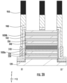
- a dummy gate structure 946 may be formed on the substrate 120.
- the dummy gate structure 946 may be formed on the preliminary stack structure 332.
- the dummy gate structure 946 may traverse the upper channel layers 336 in the Y-direction.
- the dummy gate structure 946 may include a dummy gate insulator 942 formed from the dummy gate insulator 342 on the upper channel layers 336 by an etching process, a dummy gate layer 948 on the dummy gate insulator 942, and a dummy gate mask 950 on the dummy gate layer 948.
- the dummy gate insulator 942 may include oxide (e.g., SiO 2 ), the dummy gate layer 948 may include silicon (e.g., Si), and the dummy gate mask 950 may include silicon nitride (e.g., SiN). In some embodiments, the dummy gate insulator 942 may expose at least a portion of an upper surface of the uppermost upper channel layer 336.
- the integrated sacrificial layer 318 may be removed to form an integrated insulator opening 1018.
- the integrated sacrificial layer 318 may be removed by etch process(es) (e.g., a wet etch process and/or a dry etch process).
- a preliminary gate spacer layer 1126 may be formed on the preliminary stack structure 332, on the dummy gate structure 946, and in the integrated insulator opening 1018.
- the preliminary gate spacer layer 1126 may be conformally formed on a top surface and side surfaces of the dummy gate structure 946 (e.g., dummy gate insulator 942, dummy gate layer 948, and dummy gate mask 950).
- a portion of the preliminary gate spacer layer 1126 formed in the integrated insulator opening 1018 may form the integrated insulator 118.
- the preliminary gate spacer layer 1126 may fill the integrated insulator opening 1018 to form the integrated insulator 118.
- the integrated insulator 118 may include multiple layers having different materials.
- the preliminary gate spacer layer 1126 may include, for example, siliconboron carbonitride (SiBCN) and/or silicon oxycarbonitride (SiOCN).
- an etch process may be performed on the preliminary stack structure 332 using the dummy gate structures 946 and the preliminary gate spacer layers 1126 formed on side surfaces of the dummy gate structures 946 as an etch mask, thereby forming upper channel regions 108, lower channel regions 106 and an integrated insulator 118.
- the etch process may etch a portion (e.g., an upper portion) of the preliminary gate spacer layers 1126 to form preliminary gate spacers 1226.
- an upper portion of the preliminary gate spacer 1226 may have smaller width in X-direction and/or Y-direction than that of a lower portion of the preliminary gate spacer 1226.
- the etch process may be a single process or multiple processes.
- the upper channel region 108 may be a portion of the upper channel layer 336, and the lower channel region 106 may be a portion of the lower channel layer 334. Further, a plurality of upper sacrificial patterns 1140 may be formed from the upper sacrificial layers 340, and a plurality of lower sacrificial patterns 1138 may be formed from the lower sacrificial layers 338.
- the upper inner spacer layer 134 may be formed on side surfaces of the upper sacrificial patterns 1140, and the lower inner spacer layer 132 may be formed on side surfaces of the lower sacrificial patterns 1138.
- portions of the upper sacrificial patterns 1140 and the lower sacrificial patterns 1138 may be removed to form recesses on the side surfaces of the upper sacrificial patterns 1140 and on the side surfaces of the lower sacrificial patterns 1138 and then the upper inner spacer layer 134 and the lower inner spacer layer 132 may be formed in those recesses, respectively.
- the upper inner spacer layer 134 and the lower inner spacer layer 132 may include a same material (e.g., SiN).
- the lower source/drain regions 114 and upper source/drain regions 116 may be formed.
- the lower source/drain regions 114 may be formed on side surfaces of the lower channel regions 106, respectively.
- the lower source/drain regions 114 may be epitaxially grown from the lower channel regions 106.
- the lower channel regions 106 may include silicon (Si), and the lower source/drain regions 114 may include silicon, silicon carbide, or silicon germanium.
- upper source/drain regions 116 may be formed on side surfaces of the upper channel regions 108, respectively.
- the upper source/drain regions 116 may be epitaxially grown from the upper channel regions 108.
- the upper channel regions 108 may include silicon (Si), and the upper source/drain regions 116 may include silicon, silicon carbide, or silicon germanium.
- An insulating layer 1252 may be formed on the lower source/drain regions 114 and the upper source/drain regions 116.
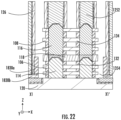
- the methods may include forming a lower gate structure and an upper gate structure (e.g., the lower gate structure 110 and the upper gate structure 112). As shown in FIGS. 13A to 13D , the dummy gate structures 946 may be removed by an etching process. In some embodiments, a first cavity (also referred to as a first opening) 1354 may be formed between the lower channel regions 106 and the intergate spacer 130 by removing the dummy gate structures 946. In some embodiments, a second cavity (also referred to as a second opening) 1356 may be formed between the intergate spacer 130 and the gate spacer 126. For example, the intergate spacer 130 may be spaced apart from the lower channel regions 106 and/or the gate spacer 126.
- the intergate spacer 130 may be spaced apart from the lower channel regions 106 and in contact with the gate spacer 126 (referring to first sub-intergate spacer 1830a in FIGS. 18A and 18B ).
- a portion of the preliminary gate spacer 1226 e.g., an upper portion of the preliminary gate spacer 1226
- the upper sacrificial patterns 1140 and the lower sacrificial patterns 1138 may be removed by an etch process.
- a gate insulator (not shown in FIGS. 13A to 13D ) having a uniform thickness may be formed along those exposed surfaces and may contact those exposed surfaces.
- the gate insulator may be formed on exposed surfaces of the lower channel regions 106 and the upper channel regions 108.
- a preliminary lower work function layer 1422 may be formed on the lower channel regions 106, upper channel regions 108, and intergate spacer 130.
- the preliminary lower work function layer 1422 may be formed in the first cavity 1354 and/or the second cavity 1356.
- the preliminary lower work function layer 1422 may at least partially fill the first cavity 1354 and/or the second cavity 1356.
- an upper portion of the preliminary lower work function layer 1422 may be removed by an etching process to form the lower work function layer 122.
- the lower work function layer 122 may be disposed on the lower channel regions 106 and the intergate spacer 130 (e.g., a side surface of the intergate spacer 130).
- a vertical portion of the lower work function layer 122 having a relatively thick thickness may be formed because of the intergate spacer 130. Accordingly, recess (e.g., pinch-off) of the lower work function layer 122 between the lower channel regions 106 may not be formed while removing the upper portion of the preliminary lower work function layer 1422. In some embodiments, an upper surface (and an upper portion of a side surface) of the intergate spacer 130 may be exposed from the lower work function layer 122.
- the upper work function layer 124 may be formed on the upper channel regions 108, intergate spacer 130 (e.g., upper surface and/or an upper portion of the intergate spacer 130), and the lower work function layer 122 (e.g., an upper surface of the lower work function layer 122).
- the gate layer 128 may be formed on the upper work function layer 124 and the upper channel regions 108.
- an upper surface of the intergate spacer 130 may be farther than an upper surface of an uppermost lower work function layer 122, an upper surface of the integrated insulator 118, and a lower surface of a lowermost upper work function layer 124 from the substrate 120 in the vertical direction.
- a lower surface of the upper channel region 108 e.g., a lower surface of the lowermost upper channel region 108 may be closer than an upper surface of the intergate spacer 130 to the substrate 120.
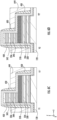
- FIGS. 17A and 17B are cross-sectional views of an integrated circuit device 170 according to some embodiments.
- the gate layer 1728 (corresponding to the gate layer 128 in FIGS. 1A to 1D ) may comprise a lower gate layer 1728a and an upper gate layer 1728b.
- the lower gate layer 1728a may be formed on the intergate spacer 130.
- the intergate spacer 130 may be between the lower work function layer 1722 and the lower gate layer 1728a.
- an upper surface of the lower work function layer 1722 and an upper surface of the lower gate layer 1728a may be at the same distance (e.g., same height) from the substrate 120, as illustrated in FIGS. 17A and 17B .
- the upper work function layer 1724 may be formed on the lower work function layer 1722, the lower gate layer 1728a, and/or the intergate spacer 130.
- the upper work function layer 1724 may contact the lower work function layer 1722 (e.g., an upper surface of the lower work function layer 1722) and the lower gate layer 1728a (e.g., an upper surface of the lower gate layer 1728a).
- the upper gate layer 1728b may be formed on the upper work function layer 1724.
- FIGS. 18A and 18B are cross-sectional views of an integrated circuit device 180 according to some embodiments.
- the integrated circuit device 180 is similar to the integrated circuit device 100 in FIGS. 1A, to 1D .
- the integrated circuit device 180 may be different from the integrated circuit device 100, in that an intergate spacer 1830 (corresponding to the intergate spacer 130 in FIGS. 1A to 1D ) may comprise multiple layers.
- the intergate spacer 1830 may include a first sub-intergate spacer 1830a and a second sub-intergate spacer 1830b.
- the first sub-intergate spacer 1830a may be disposed on the second sub-intergate spacer 1830b.
- the first sub-intergate spacer 1830a and the second sub-intergate spacer 1830b may be in contact with the gate spacer 1826 and the lower work function layer 1822.
- the first sub-intergate spacer 1830a and the second sub-intergate spacer 1830b may have different materials.
- the first sub-intergate spacer 1830a may include an insulating material, such as silicon nitride (e.g., SiN), and the second sub-intergate spacer 1830b may include a semiconductor material, such as poly-silicon.
- the embodiments of the structure, material, and location of the intergate spacer 1830 may not be limited thereto.
- FIGS. 19 through 22 are cross-sectional views illustrating methods of forming the integrated circuit device 180 in FIGS. 18A and 18B according to some embodiments.
- the methods of manufacturing the integrated circuit device 180 may include similar methods described with reference to FIGS. 3A, 3B , 3C , and 3D through 16A , 16B , 16C, and 16D .
- FIGS. 19 , 20 , 21 , and 22 may correspond to FIGS. 3A , 9A , 12A , and 13A , respectively.
- Example embodiments are described herein with reference to cross-sectional illustrations that are schematic illustrations of idealized embodiments and intermediate structures of example embodiments. As such, variations from the shapes of the illustrations as a result, for example, of manufacturing techniques and/or tolerances, are to be expected. Thus, embodiments herein should not be construed as limited to the particular shapes illustrated herein but may include deviations in shapes that result, for example, from manufacturing.
- spatially relative terms such as “beneath,” “below,” “lower,” “above,” “upper,” and the like, may be used herein for ease of description to describe one element or feature's relationship to another element(s) or feature(s) as illustrated in the figures. It will be understood that the spatially relative terms are intended to encompass different orientations of the device in use or operation in addition to the orientation depicted in the figures. For example, if a device in the figures is turned over, elements described as “below” or “beneath” other elements or features would then be oriented “above” the other elements or features. Thus, the term “below” can encompass both an orientation of above and below. The device may be otherwise oriented (e.g., rotated 90 degrees or at other orientations) and the spatially relative descriptors used herein may be interpreted accordingly.
- processes or methods may occur in a sequence different from that specified in the description herein. For example, two consecutive processes may actually be executed at the same time. Depending on a related function or operation, the processes may be executed in a reverse sequence. Moreover, a process may be separated into multiple processes and/or may be at least partially integrated.
- temporal precedent relationships between two events such as “after”, “subsequent to”, “before”, etc., another event may occur therebetween unless “directly after”, “directly subsequent” or “directly before” is not indicated.
- An integrated unitary structure herein may mean a structure formed by the same process or the same series of processes without a structurally or visibly separated sub-part therein.
Landscapes
- Insulated Gate Type Field-Effect Transistor (AREA)
- Metal-Oxide And Bipolar Metal-Oxide Semiconductor Integrated Circuits (AREA)
- Thin Film Transistor (AREA)
Applications Claiming Priority (2)
| Application Number | Priority Date | Filing Date | Title |
|---|---|---|---|
| US202363499817P | 2023-05-03 | 2023-05-03 | |
| US18/460,110 US20240371880A1 (en) | 2023-05-03 | 2023-09-01 | Integrated circuit devices including intergate spacer and methods of fabrication the same |
Publications (1)
| Publication Number | Publication Date |
|---|---|
| EP4459672A1 true EP4459672A1 (fr) | 2024-11-06 |
Family
ID=90481913
Family Applications (1)
| Application Number | Title | Priority Date | Filing Date |
|---|---|---|---|
| EP24166819.3A Pending EP4459672A1 (fr) | 2023-05-03 | 2024-03-27 | Dispositifs de circuit intégré comprenant un espaceur intergrille et leurs procédés de fabrication |
Country Status (4)
| Country | Link |
|---|---|
| US (1) | US20240371880A1 (fr) |
| EP (1) | EP4459672A1 (fr) |
| KR (1) | KR20240161015A (fr) |
| TW (1) | TW202445835A (fr) |
Citations (7)
| Publication number | Priority date | Publication date | Assignee | Title |
|---|---|---|---|---|
| US20200294866A1 (en) * | 2019-03-15 | 2020-09-17 | International Business Machines Corporation | Vertical stacked nanosheet cmos transistors with different work function metals |
| US20210265345A1 (en) * | 2020-02-22 | 2021-08-26 | International Business Machines Corporation | Stacked Nanosheet CFET with Gate All Around Structure |
| US20210320035A1 (en) * | 2020-04-14 | 2021-10-14 | International Business Machines Corporation | Work function metal patterning for nanosheet cfets |
| US20210349691A1 (en) * | 2020-05-11 | 2021-11-11 | International Business Machines Corporation | Stacked fet multiply and accumulate integrated circuit |
| US20210407999A1 (en) * | 2020-06-26 | 2021-12-30 | Intel Corporation | Stacked forksheet transistors |
| US20220109046A1 (en) * | 2020-10-02 | 2022-04-07 | Samsung Electronics Co., Ltd. | Semiconductor device having stepped multi-stack transistor structure |
| US20230055047A1 (en) * | 2021-08-17 | 2023-02-23 | International Business Machines Corporation | Semiconductor structure with embedded capacitor |
-
2023
- 2023-09-01 US US18/460,110 patent/US20240371880A1/en active Pending
-
2024
- 2024-01-30 KR KR1020240013902A patent/KR20240161015A/ko active Pending
- 2024-03-27 EP EP24166819.3A patent/EP4459672A1/fr active Pending
- 2024-03-27 TW TW113111540A patent/TW202445835A/zh unknown
Patent Citations (7)
| Publication number | Priority date | Publication date | Assignee | Title |
|---|---|---|---|---|
| US20200294866A1 (en) * | 2019-03-15 | 2020-09-17 | International Business Machines Corporation | Vertical stacked nanosheet cmos transistors with different work function metals |
| US20210265345A1 (en) * | 2020-02-22 | 2021-08-26 | International Business Machines Corporation | Stacked Nanosheet CFET with Gate All Around Structure |
| US20210320035A1 (en) * | 2020-04-14 | 2021-10-14 | International Business Machines Corporation | Work function metal patterning for nanosheet cfets |
| US20210349691A1 (en) * | 2020-05-11 | 2021-11-11 | International Business Machines Corporation | Stacked fet multiply and accumulate integrated circuit |
| US20210407999A1 (en) * | 2020-06-26 | 2021-12-30 | Intel Corporation | Stacked forksheet transistors |
| US20220109046A1 (en) * | 2020-10-02 | 2022-04-07 | Samsung Electronics Co., Ltd. | Semiconductor device having stepped multi-stack transistor structure |
| US20230055047A1 (en) * | 2021-08-17 | 2023-02-23 | International Business Machines Corporation | Semiconductor structure with embedded capacitor |
Also Published As
| Publication number | Publication date |
|---|---|
| KR20240161015A (ko) | 2024-11-12 |
| TW202445835A (zh) | 2024-11-16 |
| US20240371880A1 (en) | 2024-11-07 |
Similar Documents
| Publication | Publication Date | Title |
|---|---|---|
| CN113410236B (zh) | 铁电随机访问存储器器件和方法 | |
| TWI644363B (zh) | 半導體結構及其形成方法 | |
| US12310043B2 (en) | Method of fabricating a semiconductor device | |
| US20150311340A1 (en) | Source/Drain Profile for FinFET | |
| TW202127662A (zh) | 半導體裝置 | |
| US9543298B1 (en) | Single diffusion break structure and cuts later method of making | |
| US9536991B1 (en) | Single diffusion break structure | |
| TWI854640B (zh) | 奈米結構場效電晶體及其製造方法 | |
| US11575045B2 (en) | Semiconductor device and manufacturing method thereof | |
| US12243823B2 (en) | Semiconductor device having backside gate contact | |
| DE102022108988B4 (de) | Verfahren zur herstellung eines nanostruktur-feldeffekttransistor bauelements | |
| TW202205596A (zh) | 半導體裝置 | |
| KR20220127117A (ko) | 반도체 디바이스 및 방법 | |
| EP4333039A1 (fr) | Dispositif de circuit intégré comprenant un isolateur intégré et ses procédés de fabrication | |
| CN113745219B (zh) | 半导体器件和形成半导体器件的方法 | |
| US12249517B2 (en) | Manufacturing method of semiconductor structure | |
| CN115207107A (zh) | 半导体栅极及其形成方法 | |
| EP4459672A1 (fr) | Dispositifs de circuit intégré comprenant un espaceur intergrille et leurs procédés de fabrication | |
| CN113161353A (zh) | 半导体装置 | |
| TWI848542B (zh) | 半導體裝置及其製造方法 | |
| CN113921388B (zh) | 半导体结构的制作方法 | |
| TW202503901A (zh) | 半導體元件及其製造方法 | |
| KR20240117992A (ko) | 반도체 디바이스 및 제조 방법 | |
| CN118899315A (zh) | 集成电路装置及其制造方法 | |
| US12283527B2 (en) | Methods of forming semiconductor device structures |
Legal Events
| Date | Code | Title | Description |
|---|---|---|---|
| PUAI | Public reference made under article 153(3) epc to a published international application that has entered the european phase |
Free format text: ORIGINAL CODE: 0009012 |
|
| STAA | Information on the status of an ep patent application or granted ep patent |
Free format text: STATUS: THE APPLICATION HAS BEEN PUBLISHED |
|
| AK | Designated contracting states |
Kind code of ref document: A1 Designated state(s): AL AT BE BG CH CY CZ DE DK EE ES FI FR GB GR HR HU IE IS IT LI LT LU LV MC ME MK MT NL NO PL PT RO RS SE SI SK SM TR |
|
| STAA | Information on the status of an ep patent application or granted ep patent |
Free format text: STATUS: REQUEST FOR EXAMINATION WAS MADE |
|
| 17P | Request for examination filed |
Effective date: 20250127 |