EP4459676A2 - Module de puissance de dispositif à large bande interdite parallèle, à partage de courant, à profil bas et hautement configurable - Google Patents
Module de puissance de dispositif à large bande interdite parallèle, à partage de courant, à profil bas et hautement configurable Download PDFInfo
- Publication number
- EP4459676A2 EP4459676A2 EP24190258.4A EP24190258A EP4459676A2 EP 4459676 A2 EP4459676 A2 EP 4459676A2 EP 24190258 A EP24190258 A EP 24190258A EP 4459676 A2 EP4459676 A2 EP 4459676A2
- Authority
- EP
- European Patent Office
- Prior art keywords
- power
- power module
- module
- substrate
- contacts
- Prior art date
- Legal status (The legal status is an assumption and is not a legal conclusion. Google has not performed a legal analysis and makes no representation as to the accuracy of the status listed.)
- Pending
Links
Images


Classifications
-
- H—ELECTRICITY
- H10—SEMICONDUCTOR DEVICES; ELECTRIC SOLID-STATE DEVICES NOT OTHERWISE PROVIDED FOR
- H10W—GENERIC PACKAGES, INTERCONNECTIONS, CONNECTORS OR OTHER CONSTRUCTIONAL DETAILS OF DEVICES COVERED BY CLASS H10
- H10W90/00—Package configurations
-
- H—ELECTRICITY
- H05—ELECTRIC TECHNIQUES NOT OTHERWISE PROVIDED FOR
- H05K—PRINTED CIRCUITS; CASINGS OR CONSTRUCTIONAL DETAILS OF ELECTRIC APPARATUS; MANUFACTURE OF ASSEMBLAGES OF ELECTRICAL COMPONENTS
- H05K7/00—Constructional details common to different types of electric apparatus
- H05K7/14—Mounting supporting structure in casing or on frame or rack
- H05K7/1422—Printed circuit boards receptacles, e.g. stacked structures, electronic circuit modules or box like frames
- H05K7/1427—Housings
- H05K7/1432—Housings specially adapted for power drive units or power converters
- H05K7/14329—Housings specially adapted for power drive units or power converters specially adapted for the configuration of power bus bars
-
- H—ELECTRICITY
- H10—SEMICONDUCTOR DEVICES; ELECTRIC SOLID-STATE DEVICES NOT OTHERWISE PROVIDED FOR
- H10W—GENERIC PACKAGES, INTERCONNECTIONS, CONNECTORS OR OTHER CONSTRUCTIONAL DETAILS OF DEVICES COVERED BY CLASS H10
- H10W40/00—Arrangements for thermal protection or thermal control
- H10W40/20—Arrangements for cooling
- H10W40/22—Arrangements for cooling characterised by their shape, e.g. having conical or cylindrical projections
-
- H—ELECTRICITY
- H10—SEMICONDUCTOR DEVICES; ELECTRIC SOLID-STATE DEVICES NOT OTHERWISE PROVIDED FOR
- H10W—GENERIC PACKAGES, INTERCONNECTIONS, CONNECTORS OR OTHER CONSTRUCTIONAL DETAILS OF DEVICES COVERED BY CLASS H10
- H10W90/00—Package configurations
- H10W90/701—Package configurations characterised by the relative positions of pads or connectors relative to package parts
Definitions
- the present invention relates to improvements in wide band gap power modules. More particularly, the invention relates to improvements particularly suited for providing a configurable consistent power module design for multiple applications. In particular, the present invention relates specifically to a parallel path power module allowing for current sharing at high switching frequencies.
- Patents with information of interest to power modules include: United States Patent No. 7,687,903, issued to Son, et al. on March 30, 2010 entitled Power module and method of fabricating the same; United States Patent 7,786,486 issued to Casey, et al. on August 31, 2010 entitled Double-sided package for power module; United States Patent No. 8,018,056 issued to Hauenstein on September 13, 2011 entitled Package for high power density devices; United States Patent No. 8,368,210 issued to Hauenstein on February 5, 2013 entitled Wafer scale package for high power devices; United States Patent No. 6,307,755 issued to Williams, et al.
- Wide band gap power semiconductors including Silicon Carbide, SiC, and Gallium Nitride, GaN, offer numerous advantages over conventional Silicon, Si, based power electronic devices, including:
- the present invention is directed to an improved power module using parallel power devices.
- a power module is provided with low inductance equalized current paths to many paralleled devices, allowing for even current sharing and clean switching events.
- the power module is capable of running at junction temperatures ranging from 200 to 250°C, depending on devices, operating conditions, etc. and may carry very high currents, 100s of amps and greater.
- these enhancements fall into three categories:, 1 performance,, 2 function, and, 3 usability. This technology is designed from the ground up to embrace the characteristics and challenges of wide band gap power devices.
- Features of the power module include the following highlights:
- the power module 100 is configurable in multiple useful power electronic topologies such as half bridge, full bridge, common source, and common drain and can be configured in up to two separate channels. It is uniquely suited to take advantage of all wide band gap technology has to offer, while being flexible enough to meet the demands of many customer systems through custom configurations.
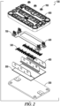
- the power module 100 consists of the primary elements outlined in Figure 2 . These include the base plate 200, power substrate 300, power contacts 400, power devices 500, gate & source kelvin interconnection board 600, gate drive connectors 700, injection molded housing 800, and fasteners 900.
- the height of the module is 2x to 3x thinner than contemporaries. It is 10mm thick in total. This dramatically reduces the module inductance and increases current carrying capability partially by utilizing lower path lengths. It may also provide a major source of system level volume savings in a power converter.
- the comparison of top size to thickness dimensions of the power module 100 are presented in Figure 3 in the top and side view comparison.
- the module 100 measures 65mm x 110mm x 10mm.
- the plastic housing 800 extends like a sheath over the base plate 200 for voltage isolation, which accounts for the extra 3mm on each side over the base plate 200 dimensions. It has a volume of 71.5cm3 and weighs approximately 140g.
- the power module 100 utilizes 57.5mm x 73mm, 42cm2, of the total footprint area for conduction. This is an impressive 60% utilization solely for current carrying. The remaining area is used for mounting, 5%, gate drive connections, 5%, and plastic features including minimum wall thickness, voltage creepage extenders, and strengthening ribs, 30%.
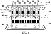
- the driving focus of the power module 100 power loop 110 is effectively paralleling large numbers of devices 500. Shown are a first power device 501, second power device 502, third power device 503, fourth power device 504, fifth power device 505, sixth power device 506, seventh power device 507, eight power device 508, ninth power device 509, tenth power device 510, and eleventh power device 511.
- the module 100 can either have two or four switch positions, depending on configuration, which is detailed later.
- Figure 4 shows the upper position 480 and the lower position 490. There is a large amount of flexibility in the formation of each switch position, such that they are tailored to specific applications without costly module 100 modifications.
- the positions may have an equal number of diodes to the power switches 500, only a few diodes, or none at all.
- Figure 4 is a representation of the power loop 110, depicting the even, shared current paths 120 for current traveling from the "V+" terminal 410 to the "Mid" terminal 420, the V- terminal 430 is also shown that is used for devices 500 in the lower position 490.
- An additional benefit of this layout is that the even spacing of each device 500 aids in the spreading of the heat sources across the module 100 instead of concentrating them in a few locations.
- the power contacts 400 were designed to have a low height such that they contribute a negligible amount to the resistance and inductance of the system.
- the low height of the power contacts 400 was achieved by using a dual bending process.
- the power contacts 400 are formed through either a metal stamping operation or by etching followed by forming in a press brake.
- the 90° bend at the base 450 creates an "L" shaped connector with a vertical body 460.
- the base 450 is soldered down to the power substrates 300.
- the base 450 is relatively thin in comparison to the overall shape. This reduces the area consumed by this bond, allowing for more active device 500 area inside of the module 100.
- staggered holes, called solder catches 454 are etched or formed along the bonding surface 452 on the bottom of the base 450. Molten solder travels up the catches 454 through capillary action. Once solidified, the solder inside of the catches 454 substantially improves bond strength in many directions.
- An exemplary contact 400 with solder catches 454 is presented in Figure 5 .
- FIG. 5 Also shown in Figure 5 is how the "L" shaped contacts 400 are bent a second time at the end of the fabrication process to form a contact top 470.
- the vertical body 460 of the contact 400 allows for a single piece plastic housing 800 to be dropped into place, as there are no undercuts present.
- the radius of the second bend 472 is not as tight as the first bend 462. This provides some tolerance in the process and is a smoother bending operation.
- the second radius 472 is facilitated through a pre-formed radius 810 in the plastic housing 800, which, at this stage, is touching the leading edge 464 of the contacts 400.
- rotating bending hardware presses flatly on the opposite surface 466, folding the contacts 400 down over the captive fasteners 900.
- An illustration of the bending of the "L” shaped contacts into “C” shaped forms is pictured in Figure 6 .
- the folded contacts 400 are low profile threaded fasteners 900 shown as nuts 900. These fasteners 900 are captured underneath the power contacts 400. They are otherwise loose.
- the captive fasteners 900 serve an important purpose. When the module 100 is bolted to buss bars, the loose fasteners 900 and the contacts 400 are pulled upwards into the bussing, creating a quality electrical connection. If the fasteners 900 were affixed to the housing 800, they would act to pull the bussing down into the module 100 and could create a poor connection due to the stiffness of the buss bars.
- the base plate 200 is a critical element of the module, providing mechanical support, heat spreading, and a means to effectively bolt down to a heat sink or cold plate.
- the material properties of the base plate 200 become increasingly important as the temperature of operation elevates.
- An effective example is found in the coefficient of thermal expansion, CTE, where materials in the assembly expand at different rates due to heat and may create large stresses in their interfaces.
- the power module 100 utilizes a Metal Matrix Composite, MMC, material, which is a composite of a high conductivity metal, copper, aluminum, etc., and either a low CTE metal such as moly, beryllium, tungsten, or a nonmetal such as silicon carbide, beryllium oxide, graphite.
- MMC Metal Matrix Composite
- Figure 7 shows how the power module 100 base plate 200 was designed to match an industry standard 62mm geometry, which has a set diameter and location for the mounting holes 203 in the corners.
- the thickness of the plate 200 was fine-tuned through the use of parametric finite element analysis of the CAD model. This was achieved by sweeping the thickness between pre-defined practical limits and measuring the thermal and mechanical responses. The material and thickness combinations that achieved the best thermal performance with a minimal mechanical deflection were selected.
- Additional features of the power module 100 plate include machined or molded, depending on the MMC material, standoffs 210 with a threaded board hole 212, and housing hole 290 each.
- the standoff 210 provides a planar surface with the power substrate 300 such that the internal gate & source kelvin board 600 can be bolted down without bowing.
- Figure 8 shows how the power module 100 and its variations include a single piece secondary substrate 600 which is placed over the power substrate 300 and then bolted down to the base plate 200.
- the gate & source kelvin substrate 600 has two interconnection channels 602, 604 which may be located in one of four positions top or first 611, upper middle or second 612, lower middle or third 613, and bottom or fourth 614 to define die apertures such as an external die aperture 603 or middle die aperture 605 to allow for a multitude of module 100 configurations.
- the relative layout of each interconnection channel 602, 604 is the same; however, the location and direction are adapted to match the associated die aperture 603, 605 and die 500 placement and rotation to match each topology.
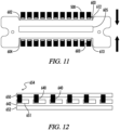
- Figure 9 Figure 10 , and Figure 11 with the arrows indicating the gate direction for a half bridge, common source, and common drain topology, respectively.
- Each of these may consist of a single or dual channel arrangement, depending on the layout of the power substrate 300 and the format of the power contacts 400 and housing 800.
- ballast resistors 640 may be included on the interconnection board 600. While there are many different layouts these boards can utilize such as parallel planes, clock tree distribution, etc., one of the more effective is a low cost single layer modular arrangement with many bonding locations 642. As shown, a gate track 650 and source track 652 go across the length of the interconnection channels 654. Source wire bonds are formed directly on the source track 652. Each gate is bonded to individual gate pads 651 which are connected to the gate track through resistors 640. The values of the resistors 640 are device and application dependent and will vary between module 100 configurations.
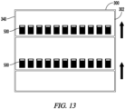
- Figure 13 shows the power substrate 300 which is a metal-ceramic-metal layered structure designed to handle very high currents and voltages with the arrows again showing the gat direction to be matched with the boards 600.
- Metals may be copper or aluminum at varying thicknesses, while the ceramic materials are typically alumina, Al203, aluminum nitride, AIN, or silicon nitride, Si3N4.
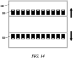
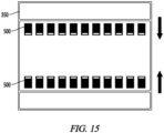
- the metal layers 302 are etched into topology specific patterns 330, 340, 350 as illustrated in Figure 13 for a half bridge substrate 330, Figure 14 for a common source substrate 340, and Figure 15 for a common drain substrate 350 showing the upper and lower die 500 positions for each configuration.
- each of these layouts may be split into a dual channel arrangement by etching a line down the center of the substrates 300. They may also be split into individual substrates per channel if desired. This may be useful for more harsh environments as the smaller substrates will experience less stress.
- the housing 800 is formed in an injection molding process with reinforced high temperature plastic.
- the housing 800 serves many functions in addition to being a protective barrier to the sensitive semiconductors 500. This includes voltage blocking, mechanical support for the captive fasteners 900, guides for the power contact bending process, entry zones for gel passivation, vents for the gel passivation process, and self-strengthening internal ribs 812. Many of these features are depicted in Figure 16 and Figure 17 .
- High aspect ratio trenches are placed around the periphery of the power contacts 400 to increase the surface distance between exposed metal contacts, increasing voltage blocking capability.
- Figure 16 shows the high temperature plastic housing topside features including the creepage extenders 802, the passivation entries and vents 804, the captive fasteners apertures 806, the labeling area 808, and the power contact pinch and radius 810.
- Figure 17 shows the backside features including the strengthening ribs 812, the thick bolt hole core sections 814, the bolt head clearance recess 816, the bottoms of the fastener insets 818, the power contact entryways 820, and the wire bond clearance apertures 822.
- FIG 18 shows how the housing 800 slides over the electronic sub assembly to form the top of the module 100, with the power contacts 400 routed through the narrow openings 820.
- the housing 800 is bolted 830 at two points to threaded holes 290 on the base plate 200.
- the gel passivation material is injected into the module 100 and fully cured.
- Multiple openings and vents 804 assist this assembly step.
- the slices 820 in the housing 800 for the power contacts 400 have drafted "guides" to aid this process, and a rounded fillet 810 on top to aid in the bending procedure. These are illustrated in Figure 19 .
- the power module 100 is configurable in a variety of useful power electronic topologies. These include half bridge, common source, and common drain. Splitting the channels, through layout changes in the power substrate 300 and gate & source kelvin board 600 and alterations to the power contacts 400 and housing 800, allows three more configurations, including a full bridge, common source dual channel, and common drain dual channel.
- Figure 20 displays the first external configuration 150 for half bridge, single channel common source, and single channel common drain configurations.
- the power contacts 400 are split and provide two fully isolated channels. Gate drive connectors 700 on both sides are now required. This arrangement is used for a full bridge, dual channel common source, and dual channel common drain topologies.
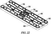
- a larger side-by-side arrangement of a dual power module 200 may be fabricated from two modules built side by side into a single housing 800. This is illustrated in Figure 22 .
Landscapes
- Engineering & Computer Science (AREA)
- Microelectronics & Electronic Packaging (AREA)
- Inverter Devices (AREA)
- Power Conversion In General (AREA)
Applications Claiming Priority (4)
| Application Number | Priority Date | Filing Date | Title |
|---|---|---|---|
| US201461933535P | 2014-01-30 | 2014-01-30 | |
| EP19189512.7A EP3582598B1 (fr) | 2014-01-30 | 2015-01-30 | Module de puissance de dispositif d'alimentation en parallèle à interstice à large bande de partage de courant, à profil bas et hautement configurable |
| EP15743771.6A EP3100301B1 (fr) | 2014-01-30 | 2015-01-30 | Module de puissance de dispositif de puissance à large bande interdite, en parallèle, à partage de courant, hautement configurable et extra-plat |
| PCT/US2015/013755 WO2015116924A1 (fr) | 2014-01-30 | 2015-01-30 | Module de puissance de dispositif de puissance à large bande interdite, en parallèle, à partage de courant, hautement configurable et extra-plat |
Related Parent Applications (2)
| Application Number | Title | Priority Date | Filing Date |
|---|---|---|---|
| EP19189512.7A Division EP3582598B1 (fr) | 2014-01-30 | 2015-01-30 | Module de puissance de dispositif d'alimentation en parallèle à interstice à large bande de partage de courant, à profil bas et hautement configurable |
| EP15743771.6A Division EP3100301B1 (fr) | 2014-01-30 | 2015-01-30 | Module de puissance de dispositif de puissance à large bande interdite, en parallèle, à partage de courant, hautement configurable et extra-plat |
Publications (2)
| Publication Number | Publication Date |
|---|---|
| EP4459676A2 true EP4459676A2 (fr) | 2024-11-06 |
| EP4459676A3 EP4459676A3 (fr) | 2025-05-14 |
Family
ID=53757754
Family Applications (3)
| Application Number | Title | Priority Date | Filing Date |
|---|---|---|---|
| EP19189512.7A Active EP3582598B1 (fr) | 2014-01-30 | 2015-01-30 | Module de puissance de dispositif d'alimentation en parallèle à interstice à large bande de partage de courant, à profil bas et hautement configurable |
| EP15743771.6A Active EP3100301B1 (fr) | 2014-01-30 | 2015-01-30 | Module de puissance de dispositif de puissance à large bande interdite, en parallèle, à partage de courant, hautement configurable et extra-plat |
| EP24190258.4A Pending EP4459676A3 (fr) | 2014-01-30 | 2015-01-30 | Module de puissance de dispositif à large bande interdite parallèle, à partage de courant, à profil bas et hautement configurable |
Family Applications Before (2)
| Application Number | Title | Priority Date | Filing Date |
|---|---|---|---|
| EP19189512.7A Active EP3582598B1 (fr) | 2014-01-30 | 2015-01-30 | Module de puissance de dispositif d'alimentation en parallèle à interstice à large bande de partage de courant, à profil bas et hautement configurable |
| EP15743771.6A Active EP3100301B1 (fr) | 2014-01-30 | 2015-01-30 | Module de puissance de dispositif de puissance à large bande interdite, en parallèle, à partage de courant, hautement configurable et extra-plat |
Country Status (3)
| Country | Link |
|---|---|
| EP (3) | EP3582598B1 (fr) |
| JP (2) | JP6573890B2 (fr) |
| WO (1) | WO2015116924A1 (fr) |
Families Citing this family (13)
| Publication number | Priority date | Publication date | Assignee | Title |
|---|---|---|---|---|
| US9839146B2 (en) * | 2015-10-20 | 2017-12-05 | Cree, Inc. | High voltage power module |
| US11652473B2 (en) | 2016-12-16 | 2023-05-16 | Wolfspeed, Inc. | Power modules having an integrated clamp circuit and process thereof |
| US11652478B2 (en) | 2016-12-16 | 2023-05-16 | Wolfspeed, Inc. | Power modules having an integrated clamp circuit and process thereof |
| US10212838B2 (en) * | 2017-01-13 | 2019-02-19 | Cree Fayetteville, Inc. | High power multilayer module having low inductance and fast switching for paralleling power devices |
| USD954667S1 (en) | 2017-01-13 | 2022-06-14 | Wolfspeed, Inc. | Power module |
| USD903590S1 (en) | 2018-09-12 | 2020-12-01 | Cree Fayetteville, Inc. | Power module |
| EP3909124A4 (fr) * | 2019-01-10 | 2022-10-26 | Wolfspeed, Inc. | Module multicouche haute puissance ayant une faible inductance et une commutation rapide pour mettre en parallèle des dispositifs de puissance |
| JP7428018B2 (ja) | 2020-03-06 | 2024-02-06 | 富士電機株式会社 | 半導体モジュール |
| US11721617B2 (en) | 2020-04-07 | 2023-08-08 | Wolfspeed, Inc. | Power module |
| US11735488B2 (en) * | 2020-04-07 | 2023-08-22 | Wolfspeed, Inc. | Power module |
| GB2619572A (en) * | 2022-06-08 | 2023-12-13 | Eaton Intelligent Power Ltd | Solid state circuit breaker |
| US12107525B1 (en) | 2023-05-08 | 2024-10-01 | Nxp Usa, Inc. | Power module with segmented output driver |
| US20250142710A1 (en) * | 2023-10-30 | 2025-05-01 | Analog Devices, Inc. | Heatsink busbar |
Citations (4)
| Publication number | Priority date | Publication date | Assignee | Title |
|---|---|---|---|---|
| US6307755B1 (en) | 1999-05-27 | 2001-10-23 | Richard K. Williams | Surface mount semiconductor package, die-leadframe combination and leadframe therefor and method of mounting leadframes to surfaces of semiconductor die |
| US7687903B2 (en) | 2007-11-16 | 2010-03-30 | Fairchild Korea Semiconductor Ltd. | Power module and method of fabricating the same |
| US7786486B2 (en) | 2005-08-02 | 2010-08-31 | Satcon Technology Corporation | Double-sided package for power module |
| US8018056B2 (en) | 2005-12-21 | 2011-09-13 | International Rectifier Corporation | Package for high power density devices |
Family Cites Families (25)
| Publication number | Priority date | Publication date | Assignee | Title |
|---|---|---|---|---|
| JPS62202548A (ja) * | 1986-02-28 | 1987-09-07 | Mitsubishi Electric Corp | 半導体装置 |
| JPH088269B2 (ja) * | 1986-10-22 | 1996-01-29 | シーメンス、アクチエンゲゼルシヤフト | 半導体デバイス |
| JPH01118454U (fr) * | 1988-02-04 | 1989-08-10 | ||
| US5038197A (en) * | 1990-06-26 | 1991-08-06 | Harris Semiconductor Patents, Inc. | Hermetically sealed die package with floating source |
| EP0838855B1 (fr) * | 1991-09-20 | 2004-11-24 | Hitachi, Ltd. | Module semi-conducteur |
| JP3396566B2 (ja) * | 1995-10-25 | 2003-04-14 | 三菱電機株式会社 | 半導体装置 |
| JPH10256411A (ja) * | 1997-03-12 | 1998-09-25 | Sansha Electric Mfg Co Ltd | 電力用半導体モジュール |
| JP3410969B2 (ja) * | 1997-06-30 | 2003-05-26 | 株式会社東芝 | 半導体装置 |
| US6060772A (en) * | 1997-06-30 | 2000-05-09 | Kabushiki Kaisha Toshiba | Power semiconductor module with a plurality of semiconductor chips |
| DE19826731C2 (de) * | 1998-06-16 | 2000-10-26 | Gruendl & Hoffmann | Halbbrückenbaugruppe |
| US6212087B1 (en) * | 1999-02-05 | 2001-04-03 | International Rectifier Corp. | Electronic half bridge module |
| JP2001185678A (ja) * | 1999-12-24 | 2001-07-06 | Toshiba Corp | 電力用半導体装置 |
| DE10019812B4 (de) * | 2000-04-20 | 2008-01-17 | Infineon Technologies Ag | Schaltungsanordnung |
| WO2002082541A1 (fr) * | 2001-04-02 | 2002-10-17 | Mitsubishi Denki Kabushiki Kaisha | Dispositif a semi-conducteur a puissance |
| JP4557507B2 (ja) * | 2002-06-13 | 2010-10-06 | パナソニック株式会社 | 半導体デバイス及びその製造方法 |
| JP2004349300A (ja) * | 2003-05-20 | 2004-12-09 | Toshiba Corp | 半導体装置及びその製造方法 |
| US7514780B2 (en) * | 2006-03-15 | 2009-04-07 | Hitachi, Ltd. | Power semiconductor device |
| JP5029078B2 (ja) * | 2006-03-15 | 2012-09-19 | 株式会社日立製作所 | 電力用半導体装置 |
| JP2010080931A (ja) * | 2008-08-27 | 2010-04-08 | Kyocera Corp | 電子部品モジュールおよびその製造方法 |
| JP5479703B2 (ja) * | 2008-10-07 | 2014-04-23 | 株式会社東芝 | 半導体装置及びその製造方法 |
| DE102009037257B4 (de) * | 2009-08-12 | 2014-07-31 | Semikron Elektronik Gmbh & Co. Kg | Leistungshalbleitermodul mit Schaltungsträger und Lastanschlusselement sowie Herstellungsverfahren hierzu |
| JP5213884B2 (ja) * | 2010-01-27 | 2013-06-19 | 三菱電機株式会社 | 半導体装置モジュール |
| JP5831626B2 (ja) * | 2012-03-28 | 2015-12-09 | 富士電機株式会社 | 半導体装置及び半導体装置の製造方法 |
| EP2833405A4 (fr) * | 2012-03-28 | 2016-01-13 | Fuji Electric Co Ltd | Dispositif à semi-conducteurs, et procédé de fabrication de celui-ci |
| JP5939055B2 (ja) * | 2012-06-28 | 2016-06-22 | 住友電気工業株式会社 | 半導体装置及び半導体装置の製造方法 |
-
2015
- 2015-01-30 WO PCT/US2015/013755 patent/WO2015116924A1/fr not_active Ceased
- 2015-01-30 JP JP2016543201A patent/JP6573890B2/ja active Active
- 2015-01-30 EP EP19189512.7A patent/EP3582598B1/fr active Active
- 2015-01-30 EP EP15743771.6A patent/EP3100301B1/fr active Active
- 2015-01-30 EP EP24190258.4A patent/EP4459676A3/fr active Pending
-
2019
- 2019-05-31 JP JP2019102377A patent/JP6891220B2/ja active Active
Patent Citations (5)
| Publication number | Priority date | Publication date | Assignee | Title |
|---|---|---|---|---|
| US6307755B1 (en) | 1999-05-27 | 2001-10-23 | Richard K. Williams | Surface mount semiconductor package, die-leadframe combination and leadframe therefor and method of mounting leadframes to surfaces of semiconductor die |
| US7786486B2 (en) | 2005-08-02 | 2010-08-31 | Satcon Technology Corporation | Double-sided package for power module |
| US8018056B2 (en) | 2005-12-21 | 2011-09-13 | International Rectifier Corporation | Package for high power density devices |
| US8368210B2 (en) | 2005-12-21 | 2013-02-05 | International Rectifier Corporation | Wafer scale package for high power devices |
| US7687903B2 (en) | 2007-11-16 | 2010-03-30 | Fairchild Korea Semiconductor Ltd. | Power module and method of fabricating the same |
Non-Patent Citations (2)
| Title |
|---|
| R. K. ULRICHW. D. BROWN: "Advanced Electronic Packaging", 2006, JOHN WILEY & SONS, INC., pages: 203 |
| SHENGNAN LI: "Ph.D. dissertation", 2011, UNIVERSITY OF TENNESSEE, article "Packaging Design of IGBT Power Module Using Novel Switching Cells" |
Also Published As
| Publication number | Publication date |
|---|---|
| JP2017504968A (ja) | 2017-02-09 |
| EP3582598A1 (fr) | 2019-12-18 |
| EP3100301A1 (fr) | 2016-12-07 |
| JP6573890B2 (ja) | 2019-09-11 |
| EP4459676A3 (fr) | 2025-05-14 |
| WO2015116924A1 (fr) | 2015-08-06 |
| EP3100301A4 (fr) | 2017-12-27 |
| EP3582598B1 (fr) | 2024-07-24 |
| JP6891220B2 (ja) | 2021-06-18 |
| EP3100301B1 (fr) | 2019-11-06 |
| JP2019140418A (ja) | 2019-08-22 |
Similar Documents
| Publication | Publication Date | Title |
|---|---|---|
| US10136529B2 (en) | Low profile, highly configurable, current sharing paralleled wide band gap power device power module | |
| EP3582598B1 (fr) | Module de puissance de dispositif d'alimentation en parallèle à interstice à large bande de partage de courant, à profil bas et hautement configurable | |
| US10405450B2 (en) | High power multilayer module having low inductance and fast switching for paralleling power devices | |
| CN105283956B (zh) | 具有竖直堆叠的半导体芯片的集成化多路输出电源转换器 | |
| US9691673B2 (en) | Power module semiconductor device | |
| CN112750800B (zh) | 半导体功率模块 | |
| US12087680B2 (en) | Power module having an elevated power plane with an integrated signal board and process of implementing the same | |
| EP3556015B1 (fr) | Modules de puissance ayant un circuit de stabilisation intégré et procédé associé | |
| US20190035771A1 (en) | Power module | |
| US11652473B2 (en) | Power modules having an integrated clamp circuit and process thereof | |
| US9095054B1 (en) | High temperature equalized electrical parasitic power packaging method for many paralleled semiconductor power devices | |
| CN101675520A (zh) | 电力用半导体模块 | |
| CN116134716A (zh) | 开关部件 | |
| CN106024764A (zh) | 具有在印刷电路板上的集成输出电感器的半导体封装体 | |
| US8933555B2 (en) | Semiconductor chip package | |
| JP5123966B2 (ja) | 半導体装置 | |
| CN207398138U (zh) | 半导体封装结构 | |
| JP7294403B2 (ja) | 半導体装置 |
Legal Events
| Date | Code | Title | Description |
|---|---|---|---|
| PUAI | Public reference made under article 153(3) epc to a published international application that has entered the european phase |
Free format text: ORIGINAL CODE: 0009012 |
|
| STAA | Information on the status of an ep patent application or granted ep patent |
Free format text: STATUS: THE APPLICATION HAS BEEN PUBLISHED |
|
| AC | Divisional application: reference to earlier application |
Ref document number: 3100301 Country of ref document: EP Kind code of ref document: P Ref document number: 3582598 Country of ref document: EP Kind code of ref document: P |
|
| AK | Designated contracting states |
Kind code of ref document: A2 Designated state(s): AL AT BE BG CH CY CZ DE DK EE ES FI FR GB GR HR HU IE IS IT LI LT LU LV MC MK MT NL NO PL PT RO RS SE SI SK SM TR |
|
| P01 | Opt-out of the competence of the unified patent court (upc) registered |
Free format text: CASE NUMBER: APP_60140/2024 Effective date: 20241107 |
|
| REG | Reference to a national code |
Ref country code: DE Ref legal event code: R079 Free format text: PREVIOUS MAIN CLASS: H01L0025070000 Ipc: H05K0007140000 |
|
| PUAL | Search report despatched |
Free format text: ORIGINAL CODE: 0009013 |
|
| AK | Designated contracting states |
Kind code of ref document: A3 Designated state(s): AL AT BE BG CH CY CZ DE DK EE ES FI FR GB GR HR HU IE IS IT LI LT LU LV MC MK MT NL NO PL PT RO RS SE SI SK SM TR |
|
| RIC1 | Information provided on ipc code assigned before grant |
Ipc: H01L 23/367 20060101ALN20250404BHEP Ipc: H01L 25/07 20060101ALI20250404BHEP Ipc: H01L 23/498 20060101ALI20250404BHEP Ipc: H05K 7/14 20060101AFI20250404BHEP |
|
| STAA | Information on the status of an ep patent application or granted ep patent |
Free format text: STATUS: REQUEST FOR EXAMINATION WAS MADE |
|
| 17P | Request for examination filed |
Effective date: 20251114 |