EP4465773A2 - Systèmes et procédés d'encapsulation de dispositifs à semi-conducteur avec des interconnexions extensibles - Google Patents
Systèmes et procédés d'encapsulation de dispositifs à semi-conducteur avec des interconnexions extensibles Download PDFInfo
- Publication number
- EP4465773A2 EP4465773A2 EP24172463.2A EP24172463A EP4465773A2 EP 4465773 A2 EP4465773 A2 EP 4465773A2 EP 24172463 A EP24172463 A EP 24172463A EP 4465773 A2 EP4465773 A2 EP 4465773A2
- Authority
- EP
- European Patent Office
- Prior art keywords
- region
- substrate
- electrical contacts
- electrical
- coupled
- Prior art date
- Legal status (The legal status is an assumption and is not a legal conclusion. Google has not performed a legal analysis and makes no representation as to the accuracy of the status listed.)
- Pending
Links
Images


Classifications
-
- H—ELECTRICITY
- H10—SEMICONDUCTOR DEVICES; ELECTRIC SOLID-STATE DEVICES NOT OTHERWISE PROVIDED FOR
- H10W—GENERIC PACKAGES, INTERCONNECTIONS, CONNECTORS OR OTHER CONSTRUCTIONAL DETAILS OF DEVICES COVERED BY CLASS H10
- H10W72/00—Interconnections or connectors in packages
- H10W72/071—Connecting or disconnecting
-
- H—ELECTRICITY
- H05—ELECTRIC TECHNIQUES NOT OTHERWISE PROVIDED FOR
- H05K—PRINTED CIRCUITS; CASINGS OR CONSTRUCTIONAL DETAILS OF ELECTRIC APPARATUS; MANUFACTURE OF ASSEMBLAGES OF ELECTRICAL COMPONENTS
- H05K1/00—Printed circuits
- H05K1/02—Details
- H05K1/11—Printed elements for providing electric connections to or between printed circuits
- H05K1/117—Pads along the edge of rigid circuit boards, e.g. for pluggable connectors
-
- G—PHYSICS
- G02—OPTICS
- G02B—OPTICAL ELEMENTS, SYSTEMS OR APPARATUS
- G02B6/00—Light guides; Structural details of arrangements comprising light guides and other optical elements, e.g. couplings
- G02B6/24—Coupling light guides
- G02B6/42—Coupling light guides with opto-electronic elements
- G02B6/4201—Packages, e.g. shape, construction, internal or external details
- G02B6/4266—Thermal aspects, temperature control or temperature monitoring
- G02B6/4268—Cooling
- G02B6/4269—Cooling with heat sinks or radiation fins
-
- G—PHYSICS
- G02—OPTICS
- G02B—OPTICAL ELEMENTS, SYSTEMS OR APPARATUS
- G02B6/00—Light guides; Structural details of arrangements comprising light guides and other optical elements, e.g. couplings
- G02B6/24—Coupling light guides
- G02B6/42—Coupling light guides with opto-electronic elements
- G02B6/4201—Packages, e.g. shape, construction, internal or external details
- G02B6/4274—Electrical aspects
- G02B6/428—Electrical aspects containing printed circuit boards [PCB]
-
- G—PHYSICS
- G02—OPTICS
- G02B—OPTICAL ELEMENTS, SYSTEMS OR APPARATUS
- G02B6/00—Light guides; Structural details of arrangements comprising light guides and other optical elements, e.g. couplings
- G02B6/24—Coupling light guides
- G02B6/42—Coupling light guides with opto-electronic elements
- G02B6/4201—Packages, e.g. shape, construction, internal or external details
- G02B6/4274—Electrical aspects
- G02B6/4284—Electrical aspects of optical modules with disconnectable electrical connectors
-
- G—PHYSICS
- G02—OPTICS
- G02B—OPTICAL ELEMENTS, SYSTEMS OR APPARATUS
- G02B6/00—Light guides; Structural details of arrangements comprising light guides and other optical elements, e.g. couplings
- G02B6/24—Coupling light guides
- G02B6/42—Coupling light guides with opto-electronic elements
- G02B6/43—Arrangements comprising a plurality of opto-electronic elements and associated optical interconnections
-
- H—ELECTRICITY
- H05—ELECTRIC TECHNIQUES NOT OTHERWISE PROVIDED FOR
- H05K—PRINTED CIRCUITS; CASINGS OR CONSTRUCTIONAL DETAILS OF ELECTRIC APPARATUS; MANUFACTURE OF ASSEMBLAGES OF ELECTRICAL COMPONENTS
- H05K1/00—Printed circuits
- H05K1/02—Details
- H05K1/14—Structural association of two or more printed circuits
- H05K1/141—One or more single auxiliary printed circuits mounted on a main printed circuit, e.g. modules, adapters
-
- H—ELECTRICITY
- H05—ELECTRIC TECHNIQUES NOT OTHERWISE PROVIDED FOR
- H05K—PRINTED CIRCUITS; CASINGS OR CONSTRUCTIONAL DETAILS OF ELECTRIC APPARATUS; MANUFACTURE OF ASSEMBLAGES OF ELECTRICAL COMPONENTS
- H05K1/00—Printed circuits
- H05K1/02—Details
- H05K1/14—Structural association of two or more printed circuits
- H05K1/144—Stacked arrangements of planar printed circuit boards
-
- H—ELECTRICITY
- H10—SEMICONDUCTOR DEVICES; ELECTRIC SOLID-STATE DEVICES NOT OTHERWISE PROVIDED FOR
- H10W—GENERIC PACKAGES, INTERCONNECTIONS, CONNECTORS OR OTHER CONSTRUCTIONAL DETAILS OF DEVICES COVERED BY CLASS H10
- H10W90/00—Package configurations
-
- H—ELECTRICITY
- H05—ELECTRIC TECHNIQUES NOT OTHERWISE PROVIDED FOR
- H05K—PRINTED CIRCUITS; CASINGS OR CONSTRUCTIONAL DETAILS OF ELECTRIC APPARATUS; MANUFACTURE OF ASSEMBLAGES OF ELECTRICAL COMPONENTS
- H05K1/00—Printed circuits
- H05K1/02—Details
- H05K1/0274—Optical details, e.g. printed circuits comprising integral optical means
-
- H—ELECTRICITY
- H05—ELECTRIC TECHNIQUES NOT OTHERWISE PROVIDED FOR
- H05K—PRINTED CIRCUITS; CASINGS OR CONSTRUCTIONAL DETAILS OF ELECTRIC APPARATUS; MANUFACTURE OF ASSEMBLAGES OF ELECTRICAL COMPONENTS
- H05K2201/00—Indexing scheme relating to printed circuits covered by H05K1/00
- H05K2201/04—Assemblies of printed circuits
- H05K2201/041—Stacked PCBs, i.e. having neither an empty space nor mounted components in between
-
- H—ELECTRICITY
- H05—ELECTRIC TECHNIQUES NOT OTHERWISE PROVIDED FOR
- H05K—PRINTED CIRCUITS; CASINGS OR CONSTRUCTIONAL DETAILS OF ELECTRIC APPARATUS; MANUFACTURE OF ASSEMBLAGES OF ELECTRICAL COMPONENTS
- H05K2201/00—Indexing scheme relating to printed circuits covered by H05K1/00
- H05K2201/04—Assemblies of printed circuits
- H05K2201/049—PCB for one component, e.g. for mounting onto mother PCB
-
- H—ELECTRICITY
- H05—ELECTRIC TECHNIQUES NOT OTHERWISE PROVIDED FOR
- H05K—PRINTED CIRCUITS; CASINGS OR CONSTRUCTIONAL DETAILS OF ELECTRIC APPARATUS; MANUFACTURE OF ASSEMBLAGES OF ELECTRICAL COMPONENTS
- H05K2201/00—Indexing scheme relating to printed circuits covered by H05K1/00
- H05K2201/10—Details of components or other objects attached to or integrated in a printed circuit board
- H05K2201/10007—Types of components
- H05K2201/10121—Optical component, e.g. opto-electronic component
-
- H—ELECTRICITY
- H05—ELECTRIC TECHNIQUES NOT OTHERWISE PROVIDED FOR
- H05K—PRINTED CIRCUITS; CASINGS OR CONSTRUCTIONAL DETAILS OF ELECTRIC APPARATUS; MANUFACTURE OF ASSEMBLAGES OF ELECTRICAL COMPONENTS
- H05K2201/00—Indexing scheme relating to printed circuits covered by H05K1/00
- H05K2201/10—Details of components or other objects attached to or integrated in a printed circuit board
- H05K2201/10613—Details of electrical connections of non-printed components, e.g. special leads
- H05K2201/10621—Components characterised by their electrical contacts
- H05K2201/10734—Ball grid array [BGA]; Bump grid array
Definitions
- the present invention is directed to semiconductor devices and packages.
- High-performance computation systems specifically those designed for machine learning and artificial intelligence applications, demand efficient and robust interconnect solutions to enable seamless communication between various computational modules. These systems are often constructed with large arrays of interconnected semiconductor devices containing multiple computational modules.
- the present invention is directed to semiconductor devices and packages.
- one or more substrate extensions are coupled to a base substrate, with portions of one or more substrates extending beyond the base substrate. Electrical and/or optical connections are connected to these substrate extensions.
- electrical and/or optical connections are connected to these substrate extensions.
- One of the design challenges in these systems is to enable module and board designs to accommodate both electrical (e.g., copper) and optical (e.g., fiber) interconnections.
- Some of the existing approaches involve routing high-speed data paths from the computational die through the module substrate to the motherboard and laterally along the motherboard to a faceplate using differential electrical signaling.
- standardized sockets allow for the use of pluggable cables to establish board-to-board connections via passive copper cables (E-to-E connection) or active optical cables (E-to-O transition). While this approach has been widely adopted, it introduces added complexity and parasitic losses associated with routing the signals through the module and motherboard.
- co-packaging of optical and electrical components in a semiconductor device refers to the process of integrating optical and electrical components in a single package.
- the package protects the semiconductor die, connects the chip to a board or other chips, and may dissipate heat.
- Copackaging of optical and electrical components is a promising technology for high-speed data transmission and processing in data centers. It can reduce the power consumption and latency of data transmission and improve the performance of data processing.
- existing copackaging approaches usually need unique module designs for optical and electrical connections.
- module-to-board edge connections involve fanning out signals from the top side of the module (where the SerDes circuitry is located), transitioning down through the module to solder ball connections on the printed circuit board (PCB) along the module's lower perimeter, and then transporting signals along planar differential transmission lines to the board edge.
- Customization of board-to-board connections between optical and electrical signaling is generally accomplished through the use of standardized cage connectors at the board edge designed to handle either pluggable electrical (e.g., passive or active) cables or pluggable (active) optical cables.
- copackaged connections as used in various existing approaches, take up a significant amount of area and perimeter on the module substrate, posing further challenges in system design.
- any element in a claim that does not explicitly state "means for” performing a specified function, or “step for” performing a specific function, is not to be interpreted as a "means” or “step” clause as specified in 35 U.S.C. Section 112, Paragraph 6.
- the use of "step of' or “act of” in the Claims herein is not intended to invoke the provisions of 35 U.S.C. 112, Paragraph 6.
- a layer can be a single layer or include multiple layers.
- a conductive layer may comprise multiple different conductive materials or multiple layers of different conductive materials
- a dielectric layer may comprise multiple dielectric materials or multiple layers of dielectric materials.
- left, right, front, back, top, bottom, forward, reverse, clockwise and counterclockwise are used for purposes of explanation only and are not limited to any fixed direction or orientation. Rather, they are used merely to indicate relative locations and/or directions between various parts of an object and/or components.
- the phrase "at least one of” preceding a series of items, with the term “and” or “or” to separate any of the items, modifies the list as a whole, rather than each member of the list (i.e., each item).
- the phrase "at least one of” does not require selection of at least one of each item listed; rather, the phrase allows a meaning that includes at least one of any one of the items, and/or at least one of any combination of the items.
- the phrases “at least one of A, B, and C" or “at least one of A, B, or C” each refer to only A, only B, or only C; and/or any combination of A, B, and C. In instances where it is intended that a selection be of "at least one of each of A, B, and C," or alternatively, "at least one of A, at least one of B, and at least one of C,” it is expressly described as such.
- FIGs 1A and 1B are diagrams illustrating a semiconductor device with extension substrates according to embodiments of the present invention. These diagrams merely provide an example, which should not unduly limit the scope of the claims.
- the terms “substrate” and “extension substrate” can refer to a circuit board, such as a printed circuit board (PCB), on which integrated circuits and other electrical components are mounted. These substrates provide a stable platform for the components, along with the necessary electrical connections for them to interact and function as a complete system.
- PCB printed circuit board
- semiconductor device 100 illustrates a packaging platform that could be customized by selection of electrical or optical soldered substrate extensions for top-side compliant connection of high-speed serial data paths.
- substrate extensions would move jumpers to the edge of the base substrate (e.g., base substrate 101), where passive E-E or O-O connectors (respectively) would connect at a faceplate to board-to-board cables.
- the interior module electronics e.g., electronic devices 141, 142, 143, and 14
- base substrate would be similar to existing approaches (e.g., compared to existing approaches) for either the electrical or optical data path configurations.
- semiconductors with substrate extensions may be used to implement serializer-deserializer (SerDes) circuitries, where SerDes may be designed with sufficient drive power to drive the entire module-to-module channel between boards or to provide direct drive to the copackaged optics.
- SerDes serializer-deserializer
- the base substrate may be different from existing approaches in three ways: first, it comprises sets of electrical connection points on the top surface for both electrical and optical extension substrates (e.g., connected to internal electronics via differential traces through the substrate's upper routing layers); second, it may lack electrical paths for these signals to the circuit board; and third, it may have reduced size and complexity by replacing vertical routing and signal fanout with simpler surface routing of signal traces and eliminating the need for co-packaged elements on the substrate surface.
- Figure 1B provides a top view of semiconductor device 100.
- semiconductor device 100 may also be referred to as semiconductor package, or a packaging platform.
- the semiconductor device comprises a first substrate 101, commonly referred to as a base substrate.
- Base substrate 101 features a top surface and a bottom surface, both of which may comprise electrical contacts.
- the top surface includes electrical contacts 103, 104, and 105 as depicted, while the bottom surface has various electrical contacts, including electrical contact 102.
- the top surface of base substrate 101 features a first region 101A on the left, a second region 101B on the right, and a third region 101C positioned between the first region 101A and the second region 101B.
- Each of these regions contains multiple electrical contacts.
- the first region 101A includes electrical contacts (e.g., electrical contact 103) for coupling to a second substrate 110
- the second region 101B contains electrical contacts (e.g., electrical contact 104) for coupling to a third substrate 120.
- the second substrate 110 and third substrate 120 may be referred to as substrate extensions, as respective portions of these substrates extend beyond the areas of base substrate 101. It is to be appreciated that substrate extensions expand the top surface area of the base substrate, creating additional space for the co-packaged elements. Substrate extensions allow for increased flexibility and customization in the design of semiconductor devices, accommodating both electrical and optical I/O components.
- the base substrate can be customized for electrical and/or optical connections, with or without substrate extensions extending beyond the areas of the base substrate.
- substrate extension 110 comprises components for electrical connections.
- Substrate extension 110 includes two regions: one region is positioned between region 101A of base substrate 101 and stiffener ring region 130A, and the other region extends beyond region 101A of base substrate 101, being coupled to electrical connector 111 (e.g., a copper connector).
- Electrical connector 111 is connected to electrical connections or wires.
- Substrate extension 110 is thermally coupled to stiffener ring region 130A via thermal interface material (TIM) 131A.
- TIM thermal interface material
- thermal interface material can refer to a substance that facilitates heat transfer between multiple surfaces or components.
- electrical connector 111 may include miniature differential cable connectors, which may be used with 78 and 95-ohm conductor cables and operate from 0 to 200 MHz.
- substrate extension 110 may include a connection site (e.g., 1.6mm miniature differential cable connection site) to accommodate miniature differential cable connections.
- stiffener ring region 130A is a portion of a stiffener ring that secures substrate extensions and provides mechanical support to base substrate 101.
- the stiffener ring is configured at the outer region of base substrate 101.
- region 130A is coupled to (and secures) substrate extension 110
- region 130B is coupled to (and secures) substrate extension 120
- regions 130C and 130D are coupled to (and provide support for) base substrate 101.
- the term “stiffener ring” refers to a component in semiconductor packages that supports electronic component packages, thereby reducing warpage.
- a stiffener ring is mounted on the top surface of the package substrate and features a reinforcement rib that is coplanar with the stiffener ring on the top surface of the package substrate.
- a stiffener ring may be configured in various shapes, and depending on the context, a stiffener ring may also be referred to as a "stiffener member".
- stiffener ring or stiffener member may be located within the extension substrate (between the extension substrate and the internal electronics), or it might not be present at all, as in the case of a lidded package.
- Second region 101B of base substrate 101 is coupled to substrate extension 120.
- Substrate extension 120 comprises components for optical connections and includes two regions: one region is positioned between region 101B of base substrate 101 and stiffener ring region 130B, while the other region extends beyond region 101B of base substrate 101 and is coupled to an optical circuit 121.
- Optical circuit 121 is designed to convert electrical signals to optical and vice versa, and it is connected to optical connector 123 via interface 122.
- optical connector 123 includes optical jumpers and/or other components.
- Substrate extension 120 is thermally coupled to stiffener ring region 130B via thermal interface material (TIM) 131B.
- TIM thermal interface material
- Third region 101C of base substrate 101 is coupled to circuit 140 via electrical connections (e.g., including electrical connection 105) and is positioned between regions 101A and 101B. Additional electronic components 141, 142, 143, and 144 are connected to circuit 140.
- Substrate extensions establish electrical signal connections to the base module through solder bumps, similar to those used to connect electronic microchips to the module in flip-chip configurations.
- the solder bump array for the extension board connections has an identical pattern for connecting to an extension board routing signals to an array connector for differential-pair electrical cables or for connecting to an extension board routing signals and power to an optical engine driving an optical fiber array.
- materials other than solder e.g., nano-particulate copper paste
- the substrate extensions comprise materials and routing layers designed for planar routing of high-frequency signals across differential signal pair conductor traces. These materials are selected to ensure a close thermal expansion match between the substrate extensions and the base-module substrate.
- the conductor and insulator layers thicknesses on the substrate extensions can be designed independently from those of the base substrate to optimize efficient longer-distance transport of high-speed signals on the substrate extensions compared to transport across the base substrate.
- Substrate extensions can overlap beyond the base module substrate's edges, optionally increasing the area available for the electrical cable array connector or the optical engine without enlarging the base module. If the extension beyond the base substrate edge is significant, a standoff element can be added for mechanical support between the motherboard and the overhanging extension board.
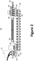
- FIG. 2 is a simplified diagram illustrating electrical connections of a semiconductor device with extension substrates according to embodiments of the present invention.
- electronic component 241 is connected to electrical connector 211 via data path 260.
- Data path 260 traverses through circuit 240, base substrate 201, and substrate extension 210, establishing a connection between electronic component 241 and electrical connector 211.
- circuit 240 may be optional and serves as an interposer, which may be implemented using silicon interposer, organic interposer, organic interposer with embedded elements, or others.
- Figure 2 shows an implementation variation compared to Figure 1 : the optical circuitry is positioned beneath the stiffener ring, enabling the stiffener ring to provide thermal management for optical circuits.
- electronic component 242 is connected to optical circuit 221 through data path 261.
- Data path 261 passes through circuit 240, base substrate 201, and substrate extension 220, providing a connection between electronic component 242 and optical circuit 221.
- Optical circuit 221 converts electrical signals to optical signals for transmission at optical connector 223 and also converts received optical signals at optical connector 223 to electrical signals.
- data paths to optical and electrical connectors meet various operating parameters.
- data paths in embodiments of the present invention comprise top-side paths for high-speed signals, while other signals may remain within the base substrate.
- the base substrate can be simplified, potentially reducing layers or area.
- Data path signaling on the top side of the base substrate connects interior electronics (e.g., interposer) with soldered substrate extensions.
- the layer composition of substrate extension boards can be optimized based on different operating parameters, such as electrical boards featuring double-height top and bottom SerDes routing without power routing, and optical boards with greater insertion loss tolerance in signal routing and additional supply routing.
- power delivery concerns for the optical engine on optical extension boards are addressed, potentially without vertical connections from the optical engine to the motherboard, by reducing optical engine power through direct-drive and off-module lasers.
- heat sinks or other components may be incorporated for the optical engine on the extension board outside the stiffener.
- electrical connectors While electrical connectors are passive and do not require power delivery, optical elements may need power supplied vertically through the base substrate and the extension board.
- an optical extension substrate routes power that an electrical extension substrate does not.
- a common interface may include power connections for the optical extension substrate, which would be unused with an electrical extension substrate.
- whether power delivery to the optical elements is vertical or has lateral routing in the optical extension substrate may depend on the positioning of the optical elements relative to the base substrate. As an example, if they are on the overhanging extension outside (e.g., region 602 in Figures 1A-2 ) the base substrate area, as shown in the right of Figure lA, lateral power routing may be needed. In Figure 2 , the optical elements are positioned under the stiffener ring, allowing for vertical power routing. It is to be noted that substrate extensions may be utilized in a module without stiffener rings or in a module where the stiffener ring is positioned on the base substrate's underside rather than on top.
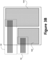
- Figures 3A and 3B are diagrams illustrating wire bending of a semiconductor device with extension substrates according to embodiments of the present invention. These diagrams merely provide an example, and should not unduly limit the scope of the claims.
- an electrical connector e.g., TwinAx
- the height needed for the curvature of the miniature differential cable stack might be prohibitive for some implementations.
- the substrate extension can reduce the miniature differential cable curvature height by dividing the cables into two bundles, thereby decreasing cable stress and improving reliability.
- Figure 3A presents a side view of two bundles of electrical connections, where bundle 312 is coupled to connection region 311A, and bundle 313 is coupled to connection region 311B.
- connection 311A and 311B are attached to substrate extension 310.
- Figure 3B offers a top view of two bundles of electrical connections coupled to two different connection regions, thus avoiding excessive bending caused by a single thick bundle.
- Figure 3A shows that bundles 312 and 313 curve around stiffener ring 330, which is connected to base substrate 301 via TIM 331.
- FIG. 4 is a simplified diagram illustrating electrical connections for an extension substrate according to embodiments of the present invention. This diagram merely provides an example, which should not unduly limit the scope of the claims.
- miniature differential cable jumper connections may be used.
- miniature differential cable jumpers may have a narrower gauge compared to board-to-board cables (e.g., 36 gauge in jumpers and 34 or higher in board-to-board cables), with a gauge conversion in the E-E connector at the faceplate.
- an additional miniature differential cable scale conversion may be used from an existing jumper scale, like 36 gauge wire on approximately 600um conductor separation, to a spacing closer to that of the 224Gbps (56GHz Nyquist PAM4) differential pair for multi-mm routes, for instance, around 200um conductor separation with suitably scaled wire.
- electrical connector 411 which may include miniature differential cable connections, is connected to substrate extension 410.
- Microcable 412 is coupled to electrical connector 411, potentially through a dense pluggable connector.
- Microcable 412 transitions to minicable 472 (e.g., a larger cable scale at 36 gauge, approximately 600um) after only a short distance (the length necessary to fan out to the larger cable).
- minicable 472 e.g., a larger cable scale at 36 gauge, approximately 600um
- the scale conversion from microcable 412 to minicable 472 may be provided "in-line,” meaning the smaller scale would transition to the larger scale independently for each cable, possibly with a permanent connection, rather than requiring a ganged connector.
- Minicable 472 transitions, at faceplate 475, into board-to-board cable 474 using a pluggable E-E scale transition (e.g., an electrical-to-electrical pluggable connection where the conductor thickness changes in gauge).
- wired connection section 470 comprises a custom-designed set of ganged cables with embedded transitions from mini to micro and a pre-defined three-dimensional shape to fit the required physical layout of the transition from the micro cable connector to the faceplate E-E connector.
- differential-pair cables used for module-to-module connections within a board may use only microscaled cables, or they might use scale-transition cables.
- Electrical substrate extensions may be used with single-scale differential pair cables (at the expense of a lower areal connection density), or transition-scale cables might be used with array connectors without extension boards, whether the connectors were direct-to-module (copackaged I/O) or connections to a board.
- a copackaged I/O solution for module-to-module routing within the board may be needed.
- This short-range routing would likely be electrical rather than optical, and could be accomplished by directly connecting copackaged electrical cables from one device's substrate extension array connector to that of another device.
- a variation might be to use a single double-ended electrical extension board as a flying bridge between devices.
- FIG. 5 is a simplified diagram illustrating a glass substrate with extension substrates according to embodiments of the present invention.
- This diagram merely provides an example, which should not unduly limit the scope of claims.
- glass substrate extension may be used to ensure accurate matching of thermal expansion coefficients.
- the use of extension boards would still provide the benefit of reducing the length of high-speed signal routing on the glass-substrate base module, enabling easier design optimization.
- a stiffener ring may not be necessary, implying that substrate extensions may not need to significantly protrude beyond the base substrate.
- substrate extension 510 mounted on base substrate 501, extends only marginally beyond the base substrate, providing an adequate contact area for mounting electrical connector 511 without a stiffener ring occupying space.
- substrate extension 520 mounted on base substrate 501, extends just slightly beyond the base substrate, offering sufficient contact area for mounting optical circuit connector 521 without the need for a stiffener ring.
- substrate extension could be glass-based if necessary for matching the coefficients of thermal expansion (CTE).
- CTE coefficients of thermal expansion
- Embodiments of the present invention offer various advantages. They enable customization of the base substrate for electrical or optical co-packaged input/output (I/O) based on the chosen substrate extensions. This differs from conventional methods that necessitate the design of the module base substrate and potentially the SerDes circuitry specifically for the type of co-packaged I/O (electrical or optical).
- these embodiments deliver high area (through substrate extensions) and connection density (through scale-transition cables) to achieve the aggregate bandwidth necessary for module-to-board edge or module-to-module within-board communication.
- existing co-packaged approaches whether optical or electrical-typically utilize one-dimensional arrays of cable or fiber connections along the module perimeter, which are insufficiently dense to meet bandwidth requirements.
- Embodiments of the present invention may be useful in distributed high-performance computing or artificial intelligence systems composed of many replicated interconnected processing modules across several equipment racks. These systems require module-to-module connections of varying lengths, with short links preferring electrical signaling for cost and power reduction, while longer links necessitate optical signaling. However, a system with high-bandwidth signaling requirements might benefit from embodiments of the present invention, even if customization of a common base module for electrical versus optical I/O is not required.
- a general aspect of the present invention includes a semiconductor device that includes a first substrate that may include a first top surface a first bottom surface.
- the first top surface may include a first region and a second region and a third region, the third region being positioned between the first region and the second region.
- the first region may include a first plurality of electrical contacts.
- the second region may include a second plurality of electrical contacts.
- the third region may include a third plurality of electrical contacts.
- the device also includes a circuit that includes a fourth plurality of electrical contacts, the fourth plurality of electrical contacts being electrically coupled to the third plurality of electrical contacts.
- the device also includes a second substrate may include a fourth region and a fifth region, the fourth region may include a fifth plurality of electrical contacts electrically coupled to the first plurality of electrical contacts, the fourth region being positioned over the first region, the fifth region being positioned outside the first substrate.
- the device also includes a third substrate may include a sixth region and a seventh region, the sixth region may include a sixth plurality of electrical contacts electrically coupled to the second plurality of electrical contacts, the sixth region being positioned over the first region, the fifth region being positioned outside the first substrate.
- the device also includes an electrical connector electrically coupled to the second substrate.
- the device also includes an optical connector electrically coupled to the third substrate.
- the circuit may be directly coupled to the first substrate using the third plurality of electrical contacts and the fourth plurality of electrical contacts.
- the circuit is positioned over the third region.
- the optical connector may include an optical circuit.
- the electrical connector may include a copper connector.
- the semiconductor device may include a plurality of electronic devices coupled to the circuit.
- the semiconductor device may include a stiffener ring, which includes an eighth region and a ninth region, the eighth region being coupled to the fourth region, the ninth region being coupled to the third region.
- the stiffener ring further may include a tenth region that is coupled to the sixth region.
- the circuit is electrically coupled to the second substrate via the first substrate.
- the semiconductor device may include a photonic integrated circuit coupled to the seventh region.
- the term "photonic integrated circuit” could refer to an integrated circuit that incorporates elements capable of interacting with light in various ways, such as processing or manipulating optical signals.
- the first bottom surface may include a seventh plurality of electrical contacts.
- the semiconductor device may include a cable jumper coupled to the second substrate.
- cable jumper may refer to a short conductor used to establish connections between different electronic components or points.
- the semiconductor device may include a fiber jumper coupled to the third substrate.
- the semiconductor device may include a thermal interface material coupled to the second substrate.
- fiber jumper may refer to a short fiber segment employed to create optical connections between various optical components.
- a semiconductor device that includes a first substrate, which may include a first top surface a first bottom surface.
- the first top surface may include a first region and a second region and a third region, the third region being positioned between the first region and the second region, the first region may include a first plurality of electrical contacts.
- the second region may include a second plurality of electrical contacts.
- the third region may include a third plurality of electrical contacts.
- the device also includes a circuit that includes a fourth plurality of electrical contacts, the fourth plurality of electrical contacts being electrically coupled to the third plurality of electrical contacts.
- the device also includes a second substrate may include a fourth region and a fifth region.
- the fourth region may include a fifth plurality of electrical contacts electrically coupled to the first plurality of electrical contacts, the fourth region being positioned over the first region, the fifth region being positioned outside the first substrate.
- the device also includes a third substrate that includes a sixth region and a seventh region.
- the sixth region may include a sixth plurality of electrical contacts electrically coupled to the second plurality of electrical contacts, the sixth region being positioned over the first region, the fifth being region positioned outside the first substrate.
- the device also includes a stiffener ring that includes an eighth region and a ninth region, the eighth region being thermally coupled to the fourth region, the ninth region being coupled to the third region.
- a semiconductor device that includes a first substrate may include a first top surface a first bottom surface, the first top surface may include a first region and a second region and a third region, the third region being positioned between the first region and the second region.
- the first region may include a first plurality of electrical contacts
- the second region may include a second plurality of electrical contacts.
- the third region may include a third plurality of electrical contacts.
- the device also includes a circuit that includes a fourth plurality of electrical contacts, the fourth plurality of electrical contacts being electrically coupled to the third plurality of electrical contacts.
- the device also includes a second substrate may include a second top region and second bottom region.
- the second substrate may include a fourth region and a fifth region, the fourth region being positioned on the second top region, the fifth region being positioned on the second bottom region.
- the fourth region may include a fifth plurality of electrical contacts electrically coupled to the first plurality of electrical contacts, the fourth region being positioned over the first region, the fifth region being positioned outside the first substrate.
- the device also includes a third substrate may include a sixth region and a seventh region, the sixth region may include a sixth plurality of electrical contacts electrically coupled to the second plurality of electrical contacts, the sixth region being positioned the first region, the fifth region positioned outside the first substrate, the seventh region may include a seventh plurality of electrical contacts.
- the device also includes an optical circuit may include an electrical interface and an optical interface, the electrical interface being coupled to the seventh plurality of electrical contacts.
Landscapes
- Physics & Mathematics (AREA)
- General Physics & Mathematics (AREA)
- Optics & Photonics (AREA)
- Engineering & Computer Science (AREA)
- Microelectronics & Electronic Packaging (AREA)
- Optical Couplings Of Light Guides (AREA)
- Combinations Of Printed Boards (AREA)
Applications Claiming Priority (1)
| Application Number | Priority Date | Filing Date | Title |
|---|---|---|---|
| US18/309,005 US12461324B2 (en) | 2023-04-28 | 2023-04-28 | Systems and methods for packaging semiconductor devices with scalable interconnects |
Publications (2)
| Publication Number | Publication Date |
|---|---|
| EP4465773A2 true EP4465773A2 (fr) | 2024-11-20 |
| EP4465773A3 EP4465773A3 (fr) | 2025-01-22 |
Family
ID=90904815
Family Applications (1)
| Application Number | Title | Priority Date | Filing Date |
|---|---|---|---|
| EP24172463.2A Pending EP4465773A3 (fr) | 2023-04-28 | 2024-04-25 | Systèmes et procédés d'encapsulation de dispositifs à semi-conducteur avec des interconnexions extensibles |
Country Status (3)
| Country | Link |
|---|---|
| US (2) | US12461324B2 (fr) |
| EP (1) | EP4465773A3 (fr) |
| CN (1) | CN118866714A (fr) |
Families Citing this family (2)
| Publication number | Priority date | Publication date | Assignee | Title |
|---|---|---|---|---|
| US12461324B2 (en) * | 2023-04-28 | 2025-11-04 | Avago Technologies International Sales Pte. Limited | Systems and methods for packaging semiconductor devices with scalable interconnects |
| US20250079276A1 (en) * | 2023-08-31 | 2025-03-06 | Advanced Micro Devices, Inc. | Stiffener with integrated connectors |
Family Cites Families (6)
| Publication number | Priority date | Publication date | Assignee | Title |
|---|---|---|---|---|
| US8971676B1 (en) * | 2013-10-07 | 2015-03-03 | Oracle International Corporation | Hybrid-integrated photonic chip package |
| JP2018518828A (ja) * | 2015-06-26 | 2018-07-12 | インテル コーポレイション | 集合化された絶縁ワイヤを含むパッケージ・アセンブリ |
| US9852988B2 (en) * | 2015-12-18 | 2017-12-26 | Invensas Bonding Technologies, Inc. | Increased contact alignment tolerance for direct bonding |
| US10748872B2 (en) * | 2017-08-22 | 2020-08-18 | Micron Technology, Inc. | Integrated semiconductor assemblies and methods of manufacturing the same |
| US11923269B2 (en) * | 2021-04-07 | 2024-03-05 | International Business Machines Corporation | Co-packaged optical module |
| US12461324B2 (en) * | 2023-04-28 | 2025-11-04 | Avago Technologies International Sales Pte. Limited | Systems and methods for packaging semiconductor devices with scalable interconnects |
-
2023
- 2023-04-28 US US18/309,005 patent/US12461324B2/en active Active
-
2024
- 2024-02-29 CN CN202410225506.6A patent/CN118866714A/zh active Pending
- 2024-04-25 EP EP24172463.2A patent/EP4465773A3/fr active Pending
-
2025
- 2025-10-08 US US19/352,837 patent/US20260036772A1/en active Pending
Also Published As
| Publication number | Publication date |
|---|---|
| US20260036772A1 (en) | 2026-02-05 |
| CN118866714A (zh) | 2024-10-29 |
| US20240361547A1 (en) | 2024-10-31 |
| US12461324B2 (en) | 2025-11-04 |
| EP4465773A3 (fr) | 2025-01-22 |
Similar Documents
| Publication | Publication Date | Title |
|---|---|---|
| US20260036772A1 (en) | Systems and methods for packaging semiconductor devices with scalable interconnects | |
| US6752539B2 (en) | Apparatus and system for providing optical bus interprocessor interconnection | |
| US8536693B2 (en) | Tiered integrated circuit assembly and a method for manufacturing the same | |
| CN100420099C (zh) | 具有栅格阵列接口的折叠式柔性电路互连器 | |
| US7470069B1 (en) | Optoelectronic MCM package | |
| US9250403B2 (en) | Hybrid-integrated photonic chip package with an interposer | |
| US20060095639A1 (en) | Structures and methods for proximity communication using bridge chips | |
| US20080008477A1 (en) | Optical transmission between devices on circuit board | |
| US8457454B1 (en) | Optical substrate chip carrier | |
| US20040218848A1 (en) | Flexible electronic/optical interconnection film assembly and method for manufacturing | |
| US20250022805A1 (en) | Optical-electrical co-package structure and communication device | |
| US7425760B1 (en) | Multi-chip module structure with power delivery using flexible cables | |
| US20240310578A1 (en) | Co-packaged optics assemblies | |
| US20100289156A1 (en) | Semiconductor device | |
| US20080080807A1 (en) | Opto-electronic connector module and opto-electronic communication module having the same | |
| US20230305244A1 (en) | High density optical/electrical interconnection arrangement with high thermal efficiency | |
| US20070217750A1 (en) | Interconnecting (mapping) a two-dimensional optoelectronic (OE) device array to a one-dimensional waveguide array | |
| US20210210478A1 (en) | Packaging solutions for high bandwidth networking applications | |
| US6705769B2 (en) | Packaging architecture for a multiple array transceiver using a flexible cable | |
| US7315669B2 (en) | Photoelectric transducer and photoelectric transducer element array | |
| JP2000269545A (ja) | 光電子集積回路装置 | |
| US7249896B2 (en) | Array optical sub-assembly | |
| US20030103737A1 (en) | Packaging architecture for a multiple array transceiver using a winged flexible cable for optimal wiring | |
| US20260093080A1 (en) | Substrate embedded optical chiplet for integrated photonic interconnects | |
| EP4636450A2 (fr) | Ensemble électro-optique double face |
Legal Events
| Date | Code | Title | Description |
|---|---|---|---|
| PUAI | Public reference made under article 153(3) epc to a published international application that has entered the european phase |
Free format text: ORIGINAL CODE: 0009012 |
|
| STAA | Information on the status of an ep patent application or granted ep patent |
Free format text: STATUS: THE APPLICATION HAS BEEN PUBLISHED |
|
| AK | Designated contracting states |
Kind code of ref document: A2 Designated state(s): AL AT BE BG CH CY CZ DE DK EE ES FI FR GB GR HR HU IE IS IT LI LT LU LV MC ME MK MT NL NO PL PT RO RS SE SI SK SM TR |
|
| PUAL | Search report despatched |
Free format text: ORIGINAL CODE: 0009013 |
|
| AK | Designated contracting states |
Kind code of ref document: A3 Designated state(s): AL AT BE BG CH CY CZ DE DK EE ES FI FR GB GR HR HU IE IS IT LI LT LU LV MC ME MK MT NL NO PL PT RO RS SE SI SK SM TR |
|
| RIC1 | Information provided on ipc code assigned before grant |
Ipc: H05K 1/02 20060101ALN20241217BHEP Ipc: H05K 1/14 20060101ALI20241217BHEP Ipc: H05K 1/11 20060101AFI20241217BHEP |
|
| STAA | Information on the status of an ep patent application or granted ep patent |
Free format text: STATUS: REQUEST FOR EXAMINATION WAS MADE |
|
| 17P | Request for examination filed |
Effective date: 20250703 |