EP4468331A1 - Structures de circuit intégré ayant des régions d'isolation en ailette contenant du métal - Google Patents
Structures de circuit intégré ayant des régions d'isolation en ailette contenant du métal Download PDFInfo
- Publication number
- EP4468331A1 EP4468331A1 EP23206672.0A EP23206672A EP4468331A1 EP 4468331 A1 EP4468331 A1 EP 4468331A1 EP 23206672 A EP23206672 A EP 23206672A EP 4468331 A1 EP4468331 A1 EP 4468331A1
- Authority
- EP
- European Patent Office
- Prior art keywords
- gate
- dielectric
- fin
- layer
- metal
- Prior art date
- Legal status (The legal status is an assumption and is not a legal conclusion. Google has not performed a legal analysis and makes no representation as to the accuracy of the status listed.)
- Pending
Links
Images









Classifications
-
- H—ELECTRICITY
- H10—SEMICONDUCTOR DEVICES; ELECTRIC SOLID-STATE DEVICES NOT OTHERWISE PROVIDED FOR
- H10D—INORGANIC ELECTRIC SEMICONDUCTOR DEVICES
- H10D84/00—Integrated devices formed in or on semiconductor substrates that comprise only semiconducting layers, e.g. on Si wafers or on GaAs-on-Si wafers
- H10D84/01—Manufacture or treatment
- H10D84/0123—Integrating together multiple components covered by H10D12/00 or H10D30/00, e.g. integrating multiple IGBTs
- H10D84/0126—Integrating together multiple components covered by H10D12/00 or H10D30/00, e.g. integrating multiple IGBTs the components including insulated gates, e.g. IGFETs
- H10D84/0151—Manufacturing their isolation regions
-
- H—ELECTRICITY
- H10—SEMICONDUCTOR DEVICES; ELECTRIC SOLID-STATE DEVICES NOT OTHERWISE PROVIDED FOR
- H10D—INORGANIC ELECTRIC SEMICONDUCTOR DEVICES
- H10D84/00—Integrated devices formed in or on semiconductor substrates that comprise only semiconducting layers, e.g. on Si wafers or on GaAs-on-Si wafers
- H10D84/80—Integrated devices formed in or on semiconductor substrates that comprise only semiconducting layers, e.g. on Si wafers or on GaAs-on-Si wafers characterised by the integration of at least one component covered by groups H10D12/00 or H10D30/00, e.g. integration of IGFETs
- H10D84/82—Integrated devices formed in or on semiconductor substrates that comprise only semiconducting layers, e.g. on Si wafers or on GaAs-on-Si wafers characterised by the integration of at least one component covered by groups H10D12/00 or H10D30/00, e.g. integration of IGFETs of only field-effect components
- H10D84/83—Integrated devices formed in or on semiconductor substrates that comprise only semiconducting layers, e.g. on Si wafers or on GaAs-on-Si wafers characterised by the integration of at least one component covered by groups H10D12/00 or H10D30/00, e.g. integration of IGFETs of only field-effect components of only insulated-gate FETs [IGFET]
- H10D84/85—Complementary IGFETs, e.g. CMOS
- H10D84/853—Complementary IGFETs, e.g. CMOS comprising FinFETs
-
- H—ELECTRICITY
- H10—SEMICONDUCTOR DEVICES; ELECTRIC SOLID-STATE DEVICES NOT OTHERWISE PROVIDED FOR
- H10D—INORGANIC ELECTRIC SEMICONDUCTOR DEVICES
- H10D30/00—Field-effect transistors [FET]
- H10D30/01—Manufacture or treatment
- H10D30/014—Manufacture or treatment of FETs having zero-dimensional [0D] or one-dimensional [1D] channels, e.g. quantum wire FETs, single-electron transistors [SET] or Coulomb blockade transistors
-
- H—ELECTRICITY
- H10—SEMICONDUCTOR DEVICES; ELECTRIC SOLID-STATE DEVICES NOT OTHERWISE PROVIDED FOR
- H10D—INORGANIC ELECTRIC SEMICONDUCTOR DEVICES
- H10D30/00—Field-effect transistors [FET]
- H10D30/40—FETs having zero-dimensional [0D], one-dimensional [1D] or two-dimensional [2D] charge carrier gas channels
- H10D30/43—FETs having zero-dimensional [0D], one-dimensional [1D] or two-dimensional [2D] charge carrier gas channels having one-dimensional [1D] charge carrier gas channels, e.g. quantum wire FETs or transistors having 1D quantum-confined channels
-
- H—ELECTRICITY
- H10—SEMICONDUCTOR DEVICES; ELECTRIC SOLID-STATE DEVICES NOT OTHERWISE PROVIDED FOR
- H10D—INORGANIC ELECTRIC SEMICONDUCTOR DEVICES
- H10D30/00—Field-effect transistors [FET]
- H10D30/60—Insulated-gate field-effect transistors [IGFET]
- H10D30/62—Fin field-effect transistors [FinFET]
- H10D30/6211—Fin field-effect transistors [FinFET] having fin-shaped semiconductor bodies integral with the bulk semiconductor substrates
-
- H—ELECTRICITY
- H10—SEMICONDUCTOR DEVICES; ELECTRIC SOLID-STATE DEVICES NOT OTHERWISE PROVIDED FOR
- H10D—INORGANIC ELECTRIC SEMICONDUCTOR DEVICES
- H10D30/00—Field-effect transistors [FET]
- H10D30/60—Insulated-gate field-effect transistors [IGFET]
- H10D30/67—Thin-film transistors [TFT]
- H10D30/6729—Thin-film transistors [TFT] characterised by the electrodes
- H10D30/673—Thin-film transistors [TFT] characterised by the electrodes characterised by the shapes, relative sizes or dispositions of the gate electrodes
- H10D30/6735—Thin-film transistors [TFT] characterised by the electrodes characterised by the shapes, relative sizes or dispositions of the gate electrodes having gates fully surrounding the channels, e.g. gate-all-around
-
- H—ELECTRICITY
- H10—SEMICONDUCTOR DEVICES; ELECTRIC SOLID-STATE DEVICES NOT OTHERWISE PROVIDED FOR
- H10D—INORGANIC ELECTRIC SEMICONDUCTOR DEVICES
- H10D30/00—Field-effect transistors [FET]
- H10D30/60—Insulated-gate field-effect transistors [IGFET]
- H10D30/67—Thin-film transistors [TFT]
- H10D30/6757—Thin-film transistors [TFT] characterised by the structure of the channel, e.g. transverse or longitudinal shape or doping profile
-
- H—ELECTRICITY
- H10—SEMICONDUCTOR DEVICES; ELECTRIC SOLID-STATE DEVICES NOT OTHERWISE PROVIDED FOR
- H10D—INORGANIC ELECTRIC SEMICONDUCTOR DEVICES
- H10D62/00—Semiconductor bodies, or regions thereof, of devices having potential barriers
- H10D62/10—Shapes, relative sizes or dispositions of the regions of the semiconductor bodies; Shapes of the semiconductor bodies
- H10D62/117—Shapes of semiconductor bodies
- H10D62/118—Nanostructure semiconductor bodies
- H10D62/119—Nanowire, nanosheet or nanotube semiconductor bodies
- H10D62/121—Nanowire, nanosheet or nanotube semiconductor bodies oriented parallel to substrates
-
- H—ELECTRICITY
- H10—SEMICONDUCTOR DEVICES; ELECTRIC SOLID-STATE DEVICES NOT OTHERWISE PROVIDED FOR
- H10D—INORGANIC ELECTRIC SEMICONDUCTOR DEVICES
- H10D84/00—Integrated devices formed in or on semiconductor substrates that comprise only semiconducting layers, e.g. on Si wafers or on GaAs-on-Si wafers
- H10D84/01—Manufacture or treatment
- H10D84/02—Manufacture or treatment characterised by using material-based technologies
- H10D84/03—Manufacture or treatment characterised by using material-based technologies using Group IV technology, e.g. silicon technology or silicon-carbide [SiC] technology
- H10D84/038—Manufacture or treatment characterised by using material-based technologies using Group IV technology, e.g. silicon technology or silicon-carbide [SiC] technology using silicon technology, e.g. SiGe
-
- H—ELECTRICITY
- H10—SEMICONDUCTOR DEVICES; ELECTRIC SOLID-STATE DEVICES NOT OTHERWISE PROVIDED FOR
- H10D—INORGANIC ELECTRIC SEMICONDUCTOR DEVICES
- H10D84/00—Integrated devices formed in or on semiconductor substrates that comprise only semiconducting layers, e.g. on Si wafers or on GaAs-on-Si wafers
- H10D84/80—Integrated devices formed in or on semiconductor substrates that comprise only semiconducting layers, e.g. on Si wafers or on GaAs-on-Si wafers characterised by the integration of at least one component covered by groups H10D12/00 or H10D30/00, e.g. integration of IGFETs
- H10D84/82—Integrated devices formed in or on semiconductor substrates that comprise only semiconducting layers, e.g. on Si wafers or on GaAs-on-Si wafers characterised by the integration of at least one component covered by groups H10D12/00 or H10D30/00, e.g. integration of IGFETs of only field-effect components
- H10D84/83—Integrated devices formed in or on semiconductor substrates that comprise only semiconducting layers, e.g. on Si wafers or on GaAs-on-Si wafers characterised by the integration of at least one component covered by groups H10D12/00 or H10D30/00, e.g. integration of IGFETs of only field-effect components of only insulated-gate FETs [IGFET]
-
- H—ELECTRICITY
- H10—SEMICONDUCTOR DEVICES; ELECTRIC SOLID-STATE DEVICES NOT OTHERWISE PROVIDED FOR
- H10D—INORGANIC ELECTRIC SEMICONDUCTOR DEVICES
- H10D84/00—Integrated devices formed in or on semiconductor substrates that comprise only semiconducting layers, e.g. on Si wafers or on GaAs-on-Si wafers
- H10D84/01—Manufacture or treatment
- H10D84/0123—Integrating together multiple components covered by H10D12/00 or H10D30/00, e.g. integrating multiple IGBTs
- H10D84/0126—Integrating together multiple components covered by H10D12/00 or H10D30/00, e.g. integrating multiple IGBTs the components including insulated gates, e.g. IGFETs
- H10D84/0135—Manufacturing their gate conductors
Definitions
- Embodiments of the disclosure are in the field of integrated circuit structures and processing and, in particular, integrated circuit structures having metal-containing fin isolation regions and methods of fabricating integrated circuit structures having metal-containing fin isolation regions.
- tri-gate transistors In the manufacture of integrated circuit devices, multi-gate transistors, such as tri-gate transistors, have become more prevalent as device dimensions continue to scale down. In conventional processes, tri-gate transistors are generally fabricated on either bulk silicon substrates or silicon-on-insulator substrates. In some instances, bulk silicon substrates are preferred due to their lower cost and because they enable a less complicated tri-gate fabrication process. In another aspect, maintaining mobility improvement and short channel control as microelectronic device dimensions scale below the 10 nanometer (nm) node provides a challenge in device fabrication. Nanowires used to fabricate devices provide improved short channel control.
- Embodiments described herein may be directed to front-end-of-line (FEOL) semiconductor processing and structures.
- FEOL is the first portion of integrated circuit (IC) fabrication where the individual devices (e.g., transistors, capacitors, resistors, etc.) are patterned in the semiconductor substrate or layer.
- FEOL generally covers everything up to (but not including) the deposition of metal interconnect layers. Following the last FEOL operation, the result is typically a wafer with isolated transistors (e.g., without any wires).
- Embodiments described herein may be directed to back-end-of-line (BEOL) semiconductor processing and structures.
- BEOL is the second portion of IC fabrication where the individual devices (e.g., transistors, capacitors, resistors, etc.) are interconnected with wiring on the wafer, e.g., the metallization layer or layers.
- BEOL includes contacts, insulating layers (dielectrics), metal levels, and bonding sites for chip-to-package connections.
- contacts pads
- interconnect wires, vias and dielectric structures are formed. For modern IC processes, more than 10 metal layers may be added in the BEOL.
- Embodiments described below may be applicable to FEOL processing and structures, BEOL processing and structures, or both FEOL and BEOL processing and structures.
- an exemplary processing scheme may be illustrated using a FEOL processing scenario, such approaches may also be applicable to BEOL processing.
- an exemplary processing scheme may be illustrated using a BEOL processing scenario, such approaches may also be applicable to FEOL processing.
- One or more embodiments described herein are directed to integrated circuit structures having fin isolation regions formed after metal gate processing, which may be referred to as post replacement gate fin trim isolation (FTI).
- One or more embodiments described herein are directed to integrated circuit structures having fin isolation regions formed prior to metal gate processing, which may be referred to as pre-replacement gate fin trim isolation (FTI).
- One or more embodiments described herein are directed to gate-all-around devices with metal-containing fin isolation regions. It is to be appreciated that, unless indicated otherwise, reference to nanowires herein can indicate nanowires or nanoribbons, or even nanosheets.
- One or more embodiments described herein are directed to FinFET structures with metal-containing fin isolation regions.
- a fin trim isolation (FTI) process is becoming very complex as the gate pitch and FIN (or wire stack) pitch is shrinking.
- FTI fin trim isolation
- a standard FTI process involves fabrication of a plug in the gate and underlying channel structures. The plug can negatively interfere with a metal gate process.
- DSA directed self-assembly
- DSA global (non-selective) gate and trench cuts
- One approach is to recess an FTI fill followed by metal cap fill; however, such an approach can be complex.
- an FTI opening is backfilled with a dielectric material after metal gate processing. At least the upper portion, if not all, of the dielectric material includes a metal such as in the form of a metal oxide.
- a metal such as in the form of a metal oxide.
- Embodiments may be implemented to provide a process flow with fewer processing operations and/or to reduce a negative impact on metal gate processing. Embodiments may be implemented to ensure an FTI structure has a gate cut around an FTI area. In an embodiment, an isotropic etch is used to remove the metal gate and then remove the fin/ribbon, followed by dielectric fill.
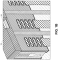
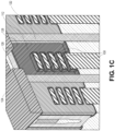
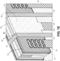
- Figures 1A-1F illustrate top-down angled cross-sectional views representing various operations in a method of fabricating an integrated circuit structure having a metal-containing fin isolation region, in accordance with an embodiment of the present disclosure. It is to be appreciated that although described in association with stacks of nanowires (or nanoribbons or nanosheets), semiconductor fins can also be covered by the embodiments, e.g., where a semiconductor fin over a sub-fin would replace a stack of nanowires over a sub-fin.
- FTI post replacement gate fin trim isolation
- a starting structure 100 includes sub-fins 104 which may be extending from a substrate, such as silicon sub-fins extending from a silicon substrate.
- the sub-fins 104 protrude through a shallow trench isolation (STI) structure 106, such as a silicon oxide structure.
- STI shallow trench isolation
- Sets of nanowires 108 are above corresponding ones of the sub-fins 104.
- Each set of nanowires 108 may be referred to as a vertical arrangement of horizontally stacked nanowires, such as a vertical arrangement of horizontally stacked silicon nanowires.
- a corresponding gate stack e.g., gate dielectric layer/gate electrode 110/112 is over each of the sets of nanowires 108, such as a gate stack including a high-k gate dielectric layer 112 and a gate electrode 110 which can include one or more conductive workfunction layers and a conductive fill material.
- Dielectric spacers 114 such as silicon nitride spacers, are along sides of the gate stack 110/112, and may be referred to as gate spacers.
- a conductive trench contact 116 is between gate spacers 114 of corresponding gate stacks.
- the conductive trench contact 116 can extend over one or more epitaxial source or drain structures (not shown, but rather is depicted in Figure 1F ), dielectric regions 118, and can have a dielectric cap 120 thereon, as is depicted.
- gate cuts are laterally adjacent to gate structures 110/112, and have dielectric gate cut plugs 122 therein (such as gate cut plugs described below).
- the starting structure 100 represents a structure following trench contact formation, replacement gate to form a permanent gate stack 110/112, and gate cut and gate cut plug formation which, in this case, is a gate cut last example.
- a photoresist layer or stack 124 is formed on structure 100 of Figure 1A .
- the photoresist layer or stack 124 is formed to have an opening 126 therein, e.g., an opening in a location where a fin trim isolation process is to be performed.
- an etch process is performed through the opening 126 to etch a trench 128.
- the etching removes the middle gate electrode 110, leaving gate dielectric layer 112 exposed.
- the trench 128 is bounded by gate cut plugs 122.
- the photoresist layer or stack 124 is removed.
- a protective helmet 129 such as a titanium helmet, is formed over the resulting structure.
- An etch process is performed through the opening in the helmet 129.
- the etching removes the nanowires 108 beneath the opening and etches into the corresponding sub-fin.
- the etching forms etched nanowire portions 108A.
- the etching can also recess the corresponding sub-fin 104 to form etch sub-fin 104A, as is depicted.
- the protective helmet 129 protects the gate spacers 114 and the gate cut plugs 122 during the etching.
- an integrated circuit structure 150 is formed by filling the cavity in the structure of Figure 1D with a dielectric structure 130, which may be referred to as a fin-trim isolation structure.
- the dielectric structure 130 does not have an associated underlying channel structure (e.g., fin, nanowire stack, etc.), while each of the remaining gate structures 110/112 has a corresponding underlying channel structure (e.g., nanowire 108 stacks), as is depicted.
- At least an upper portion of the dielectric structure 130 includes a metal, e.g., in the form of a metal oxide.
- the metal is hafnium or zirconium, or both, e.g., in the form of hafnium oxide, or zirconium oxide, or both.
- an entirety of the dielectric structure 130 is composed of a single metal-containing material, as is depicted in Figure 1E .
- a lower portion of the dielectric structure includes a dielectric material that does not include a metal
- the upper portion of the dielectric structure includes a metal-containing dielectric material, an example of which is depicted in Figure 1I .
- the metal of the metal-containing dielectric structure 130 can bind to materials used for directed self-assembly (DSA) on a metal surface. In doing, so, the metal of the metal containing dielectric structure 130 enables formation of a continuous metal-bound DSA material along an entire gate line 152 even with the larger FTI breaks therein.
- DSA material may be used as a permanent or sacrificial gate cap for later selectivity for via contact formation to trench contacts. It is to be appreciated that smaller breaks, such as gate spacers and/or gate plugs may not interfere with such DSA processing so long as the FTI structure and metal gates include metal species.
- the metal-containing dielectric structure 130 provides selectivity for etch processes, such as global gate cut processing.
- the integrated circuit structure 150 is depicted along with a structure 159 representing a rotated view of structure 150.
- epitaxial source or drain structures 132 such as epitaxial silicon germanium or epitaxial silicon source or drain structures, are viewable.
- a hardmask or protective layer can be formed over the front side of the structure.
- the structure is then subjected to backside processing.
- the backside can be planarized, e.g., for electrical coupling to a backside contact.
- an integrated circuit structure 150/159 includes a vertical stack of horizontal nanowires 108 over a first sub-fin 104.
- a gate structure 110/112 is over the vertical stack of horizontal nanowires 108 and on the first sub-fin 104.
- a dielectric structure 130 is laterally spaced apart from the gate structure 110/112. The dielectric structure 130 is not over a channel structure but is on a second sub-fin 104A.
- a gate cut is between the gate structure 110/112 and the dielectric structure 130.
- the integrated circuit structure 150/159 further includes a dielectric gate cut plug 122 in the gate cut, as is depicted.
- the integrated circuit structure 150/159 further includes a second gate structure 110/112 over a second vertical stack of horizontal nanowires 108 and on a third sub-fin 104, the second gate structure 110/112 laterally spaced apart from the dielectric structure 130 (e.g., in a direction opposite the gate structure).
- a second gate cut is between the second gate structure 110/112 and the dielectric structure 130, and a second dielectric gate cut plug 122 is in the second gate cut, as is depicted.
- the second sub-fin 104A has a top surface below a top surface of the first sub-fin 104, as is depicted.
- the integrated circuit structure 150/159 further includes an epitaxial source or drain structure 132 at an end of the vertical stack of horizontal nanowires 108, as is depicted.
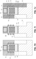
- an FTI opening is backfilled with a dielectric material prior to metal gate processing. At least the upper portion, if not all, of the dielectric material includes a metal such as in the form of a metal oxide.
- Embodiments may be implemented to provide a process flow with fewer processing operations and/or to reduce a negative impact on metal gate processing. Embodiments may be implemented to ensure an FTI structure has a gate cut around an FTI area. In an embodiment, an isotropic etch is used to remove a dummy gate and then remove the fin/ribbon, followed by dielectric fill.
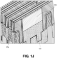
- Figures 1G-1J illustrate top-down angled cross-sectional views representing various operations in another method of fabricating an integrated circuit structure having a metal-containing fin isolation region, in accordance with another embodiment of the present disclosure. It is to be appreciated that although described in association with stacks of nanowires (or nanoribbons or nanosheets), semiconductor fins can also be covered by the embodiments, e.g., where a semiconductor fin over a sub-fin would replace a stack of nanowires over a sub-fin.
- a starting structure 160 includes nanowire stacks 162, dummy gates 164, a gate cut spacer material 166, and an opening 168 where FTI has been performed.
- the opening 168 is partially filled with a lower dielectric material 170, such as a silicon oxide or silicon dioxide material.
- a lower dielectric material 170 such as a silicon oxide or silicon dioxide material.
- the partial filling can be achieved by deposition and etch back or by bottom-up growth.
- the remainder of the opening 168 is filled with a metal-containing dielectric layer 172.
- the resulting dielectric structure 170/172 may be referred to as a fin-trim isolation structure.
- the dielectric structure 170/172 does not have an associated underlying channel structure (e.g., fin, nanowire stack, etc.), while each of the remaining dummy gate structures 164 has a corresponding underlying channel structure (e.g., nanowire 162 stacks), as is depicted.
- an upper portion 172 of the dielectric structure 170/172 includes a metal, e.g., in the form of a metal oxide.
- the metal is hafnium or zirconium, or both, e.g., in the form of hafnium oxide, or zirconium oxide, or both.
- a lower portion 170 of the dielectric structure 170/172 includes a dielectric material that does not include a metal, an example structure of which is depicted in Figure 1I .
- an entirety of a dielectric structure in place of 172/171 is composed of a single metal-containing material, such as is depicted in Figure 1E .
- the metal of the metal-containing dielectric structure 170/172 can ultimately be used to bind to materials used for directed self-assembly (DSA) on a metal surface.
- DSA directed self-assembly
- the metal of the metal containing dielectric structure 170/172 enables formation of a continuous metal-bound DSA material along an entire gate line even with the larger FTI breaks therein.
- a DSA material may be used as a permanent or sacrificial gate cap for later selectivity for via contact formation to trench contacts. It is to be appreciated that smaller breaks, such as gate spacers and/or gate plugs may not interfere with such DSA processing so long as the FTI structure and metal gates include metal species.
- the metal-containing dielectric structure 170/172 can ultimately provide selectivity for etch processes, such as global gate cut processing.
- subsequent processing can include removal of the dummy gate structure 164 to form gate cavities 174. Following that, nanowire release and permanent metal gate structure formation can be performed.
- both the gate endcap and gate cut size needs to shrink.
- Gate cut prior to gate metal fill can limit the effective end cap available for work function and can become challenging for metal fill capability in tighter space. The defect can be worse for any gate end-to-end mis-registration creating even smaller endcap space.
- any of the dielectric gate cut! gate plug structures described below may be suitable for the integrated circuit structure 150/159 described in association with Figure 1F and/or Figure 1J , or more generally for dielectric gate cut plugs 122 of Figures 1A-1F and/or Figures 1G-1J .
- Advantages for implementing approaches described herein can include a so-called "plug-last" approach with a result that a gate dielectric layer (such as a high-k gate dielectric layer) is not deposited on a gate cut plug sidewall, effectively saving additional room for work function metal deposition.
- a metal gate fill material can pinch between the plug and fin during a so-called conventional "plug-first" approach.
- the space for metal fill can be narrower due to plug mis-registration in the latter approach, and can result in voids during metal fill.
- a work function metal deposition can be seamless (e.g., void free). Nonetheless, either approach may be applicable for embodiments described herein.
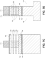
- the etch can trim the source/drain anisotropically, such as described below in association with Figure 5C .
- Such an approach may be implemented to achieve tight endcap spacing.
- a conductive gate layer 208 such as a workfunction metal layer, is over the gate dielectric material layer 206, and may be directly on the gate dielectric material layer 206 as is depicted.
- a conductive gate fill material 210 is over the conductive gate layer 208, and may be directly on the conductive gate layer 208 as is depicted.
- a dielectric gate cap 212 is on the conductive gate fill material 210.
- a dielectric gate cut plug 214 is laterally spaced apart from the fin 202 and is on the STI structure 204. The gate dielectric material layer 206 and the conductive gate layer 208 are along sides of the dielectric gate cut plug 214.
- an integrated circuit structure 250 includes a fin 252 having a portion protruding above a shallow trench isolation (STI) structure 254.
- a gate dielectric material layer 256 such as a high-k gate dielectric layer, is over the protruding portion of the fin 252 and over the STI structure 254. It is to be appreciated that, although not depicted, an oxidized portion of the fin 252 may be between the protruding portion of the fin 252 and the gate dielectric material layer 256 and may be included together with the gate dielectric material layer 256 to form a gate dielectric structure.
- a conductive gate fill material 260 is over the conductive gate layer 258, and may be directly on the conductive gate layer 258 as is depicted.
- a dielectric gate cap 262 is on the conductive gate fill material 260.
- a dielectric gate cut plug 264 is laterally spaced apart from the fin 252 and is on, but is not through, the STI structure 254.
- a dielectric plug referred to as "on but not through” an STI structure can refer to a dielectric plug landed on a top or uppermost surface of the STI, or can refer to a plug extending into but not piercing the STI.
- a plug described herein can extend entirely through, or pierce, the STI.
- the gate dielectric material layer 256 and the conductive gate layer 258 are not along sides of the dielectric gate cut plug 264. Instead, the conductive gate fill material 260 is in contact with the sides of the dielectric gate cut plug 264. As a result, a region between the dielectric gate cut plug 264 and the fin 252 includes only one layer of the gate dielectric material layer 256 and only one layer of the conductive gate layer 258, alleviating space constraints in such a tight region of the structure 250. Alleviating space constraints can improve metal fill and/or can facilitate patterning of multiple VTs.
- the dielectric gate cut plug 264 is formed after forming the gate dielectric material layer 256, the conductive gate layer 258, and the conductive gate fill material 260. As a result, the gate dielectric material layer 256 and the conductive gate layer 258 are not formed along sides of the dielectric gate cut plug 264. In an embodiment, the dielectric gate cut plug 264 has an uppermost surface co-planar with an uppermost surface of the dielectric gate cap 262, as is depicted.
- a dielectric gate cap 262 is not included, and the dielectric gate cut plug 264 has an uppermost surface co-planar with an uppermost surface of the conductive gate fill material 260, e.g., along a plane 280.
- a dielectric gate cut plug can be fabricated for a nanowire device.
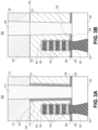
- Figure 3A illustrates a cross-sectional view of an integrated circuit structure having nanowires and a pre-metal gate dielectric plug, in accordance with an embodiment of the present disclosure.
- Figure 3B illustrates a cross-sectional view of an integrated circuit structure having nanowires and a cut metal gate dielectric plug, in accordance with an embodiment of the present disclosure.
- an oxidized portion of the sub-fin 302 and horizontally stacked nanowires 305 may be between the protruding portion of the sub-fin 302 and the gate dielectric material layer 306, and between the horizontally stacked nanowires 305 and the gate dielectric material layer 306, and may be included together with the gate dielectric material layer 306 to form a gate dielectric structure.
- a conductive gate layer 308, such as a workfunction metal layer, is over the gate dielectric material layer 306, and may be directly on the gate dielectric material layer 306 as is depicted.
- a conductive gate fill material 310 is over the conductive gate layer 308, and may be directly on the conductive gate layer 308 as is depicted.
- an integrated circuit structure 350 includes a sub-fin 352 having a portion protruding above a shallow trench isolation (STI) structure 354.
- a plurality of horizontally stacked nanowires 355 is over the sub-fin 352.
- a gate dielectric material layer 356, such as a high-k gate dielectric layer, is over the protruding portion of the sub-fin 352, over the STI structure 354, and surrounding the horizontally stacked nanowires 355.
- an oxidized portion of the sub-fin 352 may be between the protruding portion of the sub-fin 352 and the gate dielectric material layer 356, and between the horizontally stacked nanowires 355 and the gate dielectric material layer 356, and may be included together with the gate dielectric material layer 356 to form a gate dielectric structure.
- a conductive gate layer 358 such as a workfunction metal layer, is over the gate dielectric material layer 356, and may be directly on the gate dielectric material layer 356 as is depicted.
- a conductive gate fill material 360 is over the conductive gate layer 358, and may be directly on the conductive gate layer 358 as is depicted.
- a dielectric gate cap 362 is on the conductive gate fill material 360.
- a dielectric gate cut plug 364 is laterally spaced apart from the sub-fin 352 and the plurality of horizontally stacked nanowires 355, and is on, but is not through, the STI structure 354.
- the gate dielectric material layer 356 and the conductive gate layer 358 are not along sides of the dielectric gate cut plug 364. Instead, the conductive gate fill material 360 is in contact with the sides of the dielectric gate cut plug 364.
- a region between the dielectric gate cut plug 364 and the combination of the sub-fin 352 and the plurality of horizontally stacked nanowires 355 includes only one layer of the gate dielectric material layer 356 and only one layer of the conductive gate layer 358 alleviating space constraints in such a tight region of the structure 350.
- the dielectric gate cut plug 364 is formed after forming the gate dielectric material layer 356, the conductive gate layer 358, and the conductive gate fill material 360. As a result, the gate dielectric material layer 356 and the conductive gate layer 358 are not formed along sides of the dielectric gate cut plug 364.
- the dielectric gate cut plug 364 has an uppermost surface co-planar with an uppermost surface of the dielectric gate cap 362, as is depicted.
- a dielectric gate cap 362 is not included, and the dielectric gate cut plug 364 has an uppermost surface co-planar with an uppermost surface of the conductive gate fill material 360, e.g., along a plane 380.
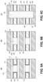
- an integrated circuit structure 550 includes gate lines between dielectric spacers 567 and conductive source or drain contacts 568.
- Each gate line includes a gate dielectric material layer 556, a conductive gate layer 558, such as a workfunction metal layer, and a conductive gate fill material 560.
- Dielectric gate cut plugs 564 can break up portions of a corresponding gate line. The dielectric gate cut plugs 564 are in contact with the conductive gate fill material 560.
- the plan view of Figure 5B may correspond to the structures of Figure 2B , 3B , or 4B . It is to be appreciated that, although referred to above as conductive source or drain contacts 568, at earlier stages of the process or in other locations of an integrated circuit structure, a placeholder dielectric or a dielectric plug is in the place of conductive source or drain contacts 568.
- SiGe silicon germanium
- Such impurities may be included as an unavoidable impurity or component during deposition of SiGe or may "contaminate" the SiGe upon diffusion during post deposition processing.
- embodiments described herein directed to a silicon germanium layer may include a silicon germanium layer that contains a relatively small amount, e.g., "impurity" level, non-Ge and non-Si atoms or species, such as carbon or tin.
- a silicon germanium layer as described herein may be undoped or may be doped with dopant atoms such as boron, phosphorous or arsenic.
- nanowires or nanoribbons, or sacrificial intervening layers may be composed of germanium.
- a germanium layer may be used to describe a germanium material composed of a very substantial amount of, if not all, germanium.
- impurities may be included as an unavoidable impurity or component during deposition of Si or may "contaminate" the Si upon diffusion during post deposition processing.
- Detection is used to identify a point when the backside surface of the donor substrate has advanced to nearly the device layer. Any endpoint detection technique known to be suitable for detecting a transition between the materials employed for the carrier layer and the intervening layer may be practiced.
- one or more endpoint criteria are based on detecting a change in optical absorbance or emission of the backside surface of the donor substrate during the polishing or etching performance. In some other embodiments, the endpoint criteria are associated with a change in optical absorbance or emission of byproducts during the polishing or etching of the donor substrate backside surface.
- absorbance or emission wavelengths associated with the carrier layer etch byproducts may change as a function of the different compositions of the carrier layer and intervening layer.
- the endpoint criteria are associated with a change in mass of species in byproducts of polishing or etching the backside surface of the donor substrate.
- the byproducts of processing may be sampled through a quadrupole mass analyzer and a change in the species mass may be correlated to the different compositions of the carrier layer and intervening layer.
- the endpoint criteria is associated with a change in friction between a backside surface of the donor substrate and a polishing surface in contact with the backside surface of the donor substrate.
- Detection of the intervening layer may be enhanced where the removal process is selective to the carrier layer relative to the intervening layer as non-uniformity in the carrier removal process may be mitigated by an etch rate delta between the carrier layer and intervening layer. Detection may even be skipped if the grind, polish and/or etch operation removes the intervening layer at a rate sufficiently below the rate at which the carrier layer is removed. If an endpoint criteria is not employed, a grind, polish and/or etch operation of a predetermined fixed duration may stop on the intervening layer material if the thickness of the intervening layer is sufficient for the selectivity of the etch.
- the carrier etch rate: intervening layer etch rate is 3:1-10:1, or more.
- the intervening layer may be removed. For example, one or more component layers of the intervening layer may be removed. A thickness of the intervening layer may be removed uniformly by a polish, for example. Alternatively, a thickness of the intervening layer may be removed with a masked or blanket etch process. The process may employ the same polish or etch process as that employed to thin the carrier, or may be a distinct process with distinct process parameters. For example, where the intervening layer provides an etch stop for the carrier removal process, the latter operation may employ a different polish or etch process that favors removal of the intervening layer over removal of the device layer.
- the removal process may be relatively slow, optimized for across-wafer uniformity, and more precisely controlled than that employed for removal of the carrier layer.
- a CMP process employed may, for example employ a slurry that offers very high selectively (e.g., 100:1-300:1, or more) between semiconductor (e.g., silicon) and dielectric material (e.g., SiO) surrounding the device layer and embedded within the intervening layer, for example, as electrical isolation between adjacent device regions.
- backside processing may commence on an exposed backside of the device layer or specific device regions there in.
- the backside device layer processing includes a further polish or wet/dry etch through a thickness of the device layer disposed between the intervening layer and a device region previously fabricated in the device layer, such as a source or drain region.
- such an etch may be a patterned etch or a materially selective etch that imparts significant non-planarity or topography into the device layer backside surface.
- the patterning may be within a device cell (i.e., "intra-cell” patterning) or may be across device cells (i.e., "inter-cell” patterning).
- at least a partial thickness of the intervening layer is employed as a hard mask for backside device layer patterning.
- a masked etch process may preface a correspondingly masked device layer etch.
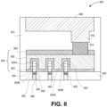
- a semiconductor structure or device 800 includes a non-planar active region (e.g., a fin structure including protruding fin portion 804 and sub-fin region 805) within a trench isolation region 806.
- the non-planar active region is separated into nanowires (such as nanowires 804A and 804B) above sub-fin region 805, as is represented by the dashed lines.
- a non-planar active region 804 is referenced below as a protruding fin portion.
- the sub-fin region 805 also includes a relaxed buffer layer 842 and a defect modification layer 840, as is depicted.
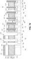
- Figure 10 illustrate cross-sectional views representing various operations in a method of fabricating a self-aligned gate endcap (SAGE) structure with gate-all-around devices, in accordance with an embodiment of the present disclosure.
- SAGE self-aligned gate endcap
- the structure of part (b) has an isolation layer 1040 and a SAGE material 1042 formed in trenches 1030.
- the structure is then planarized to leave patterned topographic masking layer 1020' as an exposed upper layer.
- the isolation layer 1040 is recessed below an upper surface of the patterned substrate 1002, e.g., to define a protruding fin portion and to provide a trench isolation structure 1041 beneath SAGE walls 1042.
- the structure of part (e) Figure 10 can be fabricated to include a metal-containing fin isolation region, examples of which are described above.
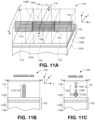
- Figure 11A illustrates a three-dimensional cross-sectional view of a nanowire-based integrated circuit structure, in accordance with an embodiment of the present disclosure.
- Figure 11B illustrates a cross-sectional source or drain view of the nanowire-based integrated circuit structure of Figure 11A , as taken along the a-a' axis.
- Figure 11C illustrates a cross-sectional channel view of the nanowire-based integrated circuit structure of Figure 11A , as taken along the b-b' axis.
- nanowire 1104A is used as an example where description is focused on one of the nanowires. It is to be appreciated that where attributes of one nanowire are described, embodiments based on a plurality of nanowires may have the same or essentially the same attributes for each of the nanowires.
- the source or drain regions 1110/1112 are non-discrete in that there are not individual and discrete source or drain regions for each channel region 1106 of a nanowire 1104. Accordingly, in embodiments having a plurality of nanowires 1104, the source or drain regions 1110/1112 of the nanowires are global or unified source or drain regions as opposed to discrete for each nanowire. That is, the non-discrete source or drain regions 1110/1112 are global in the sense that a single unified feature is used as a source or drain region for a plurality (in this case, 3) of nanowires 1104 and, more particularly, for more than one discrete channel region 1106.
- each of the pair of non-discrete source or drain regions 1110/1112 is approximately rectangular in shape with a bottom tapered portion and a top vertex portion, as depicted in Figure 11B .
- the source or drain regions 1110/1112 of the nanowires are relatively larger yet discrete non-vertically merged epitaxial structures such as nubs described in association with Figures 7A-7J .
- each of the channel regions 1106 has a width (Wc) and a height (Hc), the width (Wc) approximately the same as the height (Hc). That is, in both cases, the channel regions 1106 are square-like or, if corner-rounded, circle-like in cross-section profile. In another aspect, the width and height of the channel region need not be the same, such as the case for nanoribbons as described throughout.
- an underlying substrate may be composed of a semiconductor material that can withstand a manufacturing process and in which charge can migrate.
- the substrate is a bulk substrate composed of a crystalline silicon, silicon/germanium or germanium layer doped with a charge carrier, such as but not limited to phosphorus, arsenic, boron, gallium or a combination thereof, to form an active region.
- a charge carrier such as but not limited to phosphorus, arsenic, boron, gallium or a combination thereof.
- the concentration of silicon atoms in a bulk substrate is greater than 97%.
- a bulk substrate is composed of an epitaxial layer grown atop a distinct crystalline substrate, e.g. a silicon epitaxial layer grown atop a boron-doped bulk silicon mono-crystalline substrate.
- Embodiments disclosed herein may be used to manufacture a wide variety of different types of integrated circuits and/or microelectronic devices. Examples of such integrated circuits include, but are not limited to, processors, chipset components, graphics processors, digital signal processors, micro-controllers, and the like. In other embodiments, semiconductor memory may be manufactured. Moreover, the integrated circuits or other microelectronic devices may be used in a wide variety of electronic devices known in the arts. For example, in computer systems (e.g., desktop, laptop, server), cellular phones, personal electronics, etc. The integrated circuits may be coupled with a bus and other components in the systems. For example, a processor may be coupled by one or more buses to a memory, a chipset, etc. Each of the processor, the memory, and the chipset, may potentially be manufactured using the approaches disclosed herein.
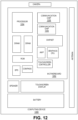
- FIG 12 illustrates a computing device 1200 in accordance with one implementation of an embodiment of the present disclosure.
- the computing device 1200 houses a board 1202.
- the board 1202 may include a number of components, including but not limited to a processor 1204 and at least one communication chip 1206.
- the processor 1204 is physically and electrically coupled to the board 1202.
- the at least one communication chip 1206 is also physically and electrically coupled to the board 1202.
- the communication chip 1206 is part of the processor 1204.
- computing device 1200 may include other components that may or may not be physically and electrically coupled to the board 1202. These other components include, but are not limited to, volatile memory (e.g., DRAM), non-volatile memory (e.g., ROM), flash memory, a graphics processor, a digital signal processor, a crypto processor, a chipset, an antenna, a display, a touchscreen display, a touchscreen controller, a battery, an audio codec, a video codec, a power amplifier, a global positioning system (GPS) device, a compass, an accelerometer, a gyroscope, a speaker, a camera, and a mass storage device (such as hard disk drive, compact disk (CD), digital versatile disk (DVD), and so forth).
- volatile memory e.g., DRAM
- non-volatile memory e.g., ROM
- flash memory e.g., a graphics processor, a digital signal processor, a crypto processor, a chipset, an antenna,
- the communication chip 1206 enables wireless communications for the transfer of data to and from the computing device 1200.
- wireless and its derivatives may be used to describe circuits, devices, systems, methods, techniques, communications channels, etc., that may communicate data through the use of modulated electromagnetic radiation through a non-solid medium. The term does not imply that the associated devices do not contain any wires, although in some embodiments they might not.
- the communication chip 1206 may implement any of a number of wireless standards or protocols, including but not limited to Wi-Fi (IEEE 802.11 family), WiMAX (IEEE 802.16 family), IEEE 802.20, long term evolution (LTE), Ev-DO, HSPA+, HSDPA+, HSUPA+, EDGE, GSM, GPRS, CDMA, TDMA, DECT, Bluetooth, derivatives thereof, as well as any other wireless protocols that are designated as 3G, 4G, 5G, and beyond.
- the computing device 1200 may include a plurality of communication chips 1206.
- another component housed within the computing device 1200 may contain an integrated circuit die that includes one or structures, such as gate-all-around integrated circuit structures having metal-containing fin isolation regions, built in accordance with implementations of embodiments of the present disclosure.
- the computing device 1200 may be a laptop, a netbook, a notebook, an ultrabook, a smartphone, a tablet, a personal digital assistant (PDA), an ultra mobile PC, a mobile phone, a desktop computer, a server, a printer, a scanner, a monitor, a set-top box, an entertainment control unit, a digital camera, a portable music player, or a digital video recorder.
- the computing device 1200 may be any other electronic device that processes data.
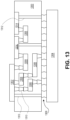
- FIG 13 illustrates an interposer 1300 that includes one or more embodiments of the present disclosure.
- the interposer 1300 is an intervening substrate used to bridge a first substrate 1302 to a second substrate 1304.
- the first substrate 1302 may be, for instance, an integrated circuit die.
- the second substrate 1304 may be, for instance, a memory module, a computer motherboard, or another integrated circuit die.
- the purpose of an interposer 1300 is to spread a connection to a wider pitch or to reroute a connection to a different connection.
- an interposer 1300 may couple an integrated circuit die to a ball grid array (BGA) 1306 that can subsequently be coupled to the second substrate 1304.
- BGA ball grid array
- first and second substrates 1302/1304 are attached to opposing sides of the interposer 1300. In other embodiments, the first and second substrates 1302/1304 are attached to the same side of the interposer 1300. And in further embodiments, three or more substrates are interconnected by way of the interposer 1300.
- the interposer 1300 may be formed of an epoxy resin, a fiberglass-reinforced epoxy resin, a ceramic material, or a polymer material such as polyimide. In further implementations, the interposer 1300 may be formed of alternate rigid or flexible materials that may include the same materials described above for use in a semiconductor substrate, such as silicon, germanium, and other group III-V and group IV materials.
- Example embodiment 1 An integrated circuit structure includes a vertical stack of horizontal nanowires over a first sub-fin.
- a gate structure is over the vertical stack of horizontal nanowires and on the first sub-fin.
- a dielectric structure is laterally spaced apart from the gate structure. The dielectric structure is not over a channel structure but is on a second sub-fin.
- a gate cut is between the gate structure and the dielectric structure.
- a dielectric gate cut plug is in the gate cut.
- the dielectric gate plug includes a metal-containing dielectric material.
- Example embodiment 3 The integrated circuit structure of example embodiment 1 or 2, further including a second gate structure over a second vertical stack of horizontal nanowires and on a third sub-fin, the second gate structure laterally spaced apart from the dielectric structure.
- a second gate cut is between the second gate structure and the dielectric structure, and a second dielectric gate cut plug is in the second gate cut.
- the second dielectric gate plug includes the metal-containing dielectric material.
- Example embodiment 4 The integrated circuit structure of example embodiment 1, 2 or 3, wherein the second sub-fin has a top surface below a top surface of the first sub-fin.
- Example embodiment 5 The integrated circuit structure of example embodiment 1, 2, 3 or 4, further including an epitaxial source or drain structure at an end of the vertical stack of horizontal nanowires.
- Example embodiment 6 An integrated circuit structure includes a fin over a first sub-fin. A gate structure is over the fin. A dielectric structure is laterally spaced apart from the gate structure. The dielectric structure is not over a channel structure but is on a second sub-fin. A gate cut is between the gate structure and the dielectric structure. A dielectric gate cut plug is in the gate cut. The dielectric gate plug includes a metal-containing dielectric material.
- a computing device includes a board, and a component coupled to the board.
- the component includes an integrated circuit structure including a vertical stack of horizontal nanowires over a first sub-fin.
- a gate structure is over the vertical stack of horizontal nanowires and on the first sub-fin.
- a dielectric structure is laterally spaced apart from the gate structure. The dielectric structure is not over a channel structure but is on a second sub-fin.
- a gate cut is between the gate structure and the dielectric structure.
- a dielectric gate cut plug is in the gate cut.
- the dielectric gate plug includes a metal-containing dielectric material.
Landscapes
- Insulated Gate Type Field-Effect Transistor (AREA)
- Metal-Oxide And Bipolar Metal-Oxide Semiconductor Integrated Circuits (AREA)
Priority Applications (1)
| Application Number | Priority Date | Filing Date | Title |
|---|---|---|---|
| EP25227035.0A EP4697896A2 (fr) | 2023-05-23 | 2023-10-30 | Structures de circuit intégré ayant des régions d'isolation d'ailette contenant du métal |
Applications Claiming Priority (1)
| Application Number | Priority Date | Filing Date | Title |
|---|---|---|---|
| US18/200,967 US20240395815A1 (en) | 2023-05-23 | 2023-05-23 | Integrated circuit structures having metal-containing fin isolation regions |
Related Child Applications (1)
| Application Number | Title | Priority Date | Filing Date |
|---|---|---|---|
| EP25227035.0A Division EP4697896A2 (fr) | 2023-05-23 | 2023-10-30 | Structures de circuit intégré ayant des régions d'isolation d'ailette contenant du métal |
Publications (1)
| Publication Number | Publication Date |
|---|---|
| EP4468331A1 true EP4468331A1 (fr) | 2024-11-27 |
Family
ID=88600201
Family Applications (2)
| Application Number | Title | Priority Date | Filing Date |
|---|---|---|---|
| EP25227035.0A Pending EP4697896A2 (fr) | 2023-05-23 | 2023-10-30 | Structures de circuit intégré ayant des régions d'isolation d'ailette contenant du métal |
| EP23206672.0A Pending EP4468331A1 (fr) | 2023-05-23 | 2023-10-30 | Structures de circuit intégré ayant des régions d'isolation en ailette contenant du métal |
Family Applications Before (1)
| Application Number | Title | Priority Date | Filing Date |
|---|---|---|---|
| EP25227035.0A Pending EP4697896A2 (fr) | 2023-05-23 | 2023-10-30 | Structures de circuit intégré ayant des régions d'isolation d'ailette contenant du métal |
Country Status (3)
| Country | Link |
|---|---|
| US (1) | US20240395815A1 (fr) |
| EP (2) | EP4697896A2 (fr) |
| CN (2) | CN121772334A (fr) |
Families Citing this family (1)
| Publication number | Priority date | Publication date | Assignee | Title |
|---|---|---|---|---|
| US12527078B2 (en) * | 2021-12-21 | 2026-01-13 | Intel Corporation | Gate-all-around integrated circuit structures having epitaxial source or drain region lateral isolation |
Citations (4)
| Publication number | Priority date | Publication date | Assignee | Title |
|---|---|---|---|---|
| US20210126113A1 (en) * | 2019-10-29 | 2021-04-29 | Taiwan Semiconductor Manufacturing Co., Ltd. | Semiconductor devices and methods of manufacture |
| US20210134797A1 (en) * | 2019-10-30 | 2021-05-06 | Taiwan Semiconductor Manufacturing Co., Ltd. | A method (and related apparatus) for forming a semiconductor device with reduced spacing between nanostructure field-effect transistors |
| US20220093592A1 (en) * | 2020-09-23 | 2022-03-24 | Intel Corporation | Fabrication of gate-all-around integrated circuit structures having pre-spacer deposition cut gates |
| US20220271139A1 (en) * | 2021-02-19 | 2022-08-25 | Taiwan Semiconductor Manufacturing Company, Ltd. | Semiconductor Device With Backside Gate Isolation Structure And Method For Forming The Same |
-
2023
- 2023-05-23 US US18/200,967 patent/US20240395815A1/en active Pending
- 2023-10-30 EP EP25227035.0A patent/EP4697896A2/fr active Pending
- 2023-10-30 EP EP23206672.0A patent/EP4468331A1/fr active Pending
- 2023-12-26 CN CN202511961408.XA patent/CN121772334A/zh active Pending
- 2023-12-26 CN CN202311801489.8A patent/CN119028971A/zh active Pending
Patent Citations (4)
| Publication number | Priority date | Publication date | Assignee | Title |
|---|---|---|---|---|
| US20210126113A1 (en) * | 2019-10-29 | 2021-04-29 | Taiwan Semiconductor Manufacturing Co., Ltd. | Semiconductor devices and methods of manufacture |
| US20210134797A1 (en) * | 2019-10-30 | 2021-05-06 | Taiwan Semiconductor Manufacturing Co., Ltd. | A method (and related apparatus) for forming a semiconductor device with reduced spacing between nanostructure field-effect transistors |
| US20220093592A1 (en) * | 2020-09-23 | 2022-03-24 | Intel Corporation | Fabrication of gate-all-around integrated circuit structures having pre-spacer deposition cut gates |
| US20220271139A1 (en) * | 2021-02-19 | 2022-08-25 | Taiwan Semiconductor Manufacturing Company, Ltd. | Semiconductor Device With Backside Gate Isolation Structure And Method For Forming The Same |
Also Published As
| Publication number | Publication date |
|---|---|
| CN119028971A (zh) | 2024-11-26 |
| EP4697896A2 (fr) | 2026-02-18 |
| CN121772334A (zh) | 2026-03-31 |
| US20240395815A1 (en) | 2024-11-28 |
Similar Documents
| Publication | Publication Date | Title |
|---|---|---|
| US12419085B2 (en) | Integrated circuit structures having backside gate tie-down | |
| EP4105978A1 (fr) | Structures de circuit intégré dotées de grilles métalliques de coupe avec remplissage d'espaceur diélectrique | |
| EP4109514A1 (fr) | Structures de circuit intégré dotées de grilles métalliques avec des bouchons coniques | |
| EP4202995A1 (fr) | Structures de circuit intégré ayant un bouchon diéléctric de grille positionné sur un ancrage diélectrique | |
| EP4195249A1 (fr) | Structures de circuit intégré ayant un décalage de coupure de grille | |
| EP4345876A1 (fr) | Structures de circuit intégré ayant des régions d'isolation d'ailette bordées par des coupes de grille | |
| EP4345875A1 (fr) | Structures de circuit intégré ayant des régions d'isolation d'ailette avec évidement pour contact de grille | |
| US20250331300A1 (en) | Integrated circuit structures having cut metal gates | |
| EP4345879A1 (fr) | Structures de circuit intégré ayant une grille métallique uniforme et une fiche de contact à tranchée | |
| EP4195251A1 (fr) | Structures de circuit intégré ayant un placement de canal polyvalent | |
| EP4199044A1 (fr) | Structures de circuit intégré ayant un ancrage diélectrique et une structure de source ou drain épitaxiale confinée | |
| US20240105802A1 (en) | Integrated circuit structures having gate cut plugremoved from trench contact | |
| EP4156244A1 (fr) | Structures de circuit intégré dotées d'une paroi de grille diélectrique et d'un bouchon de grille diélectrique | |
| EP4105991A1 (fr) | Structures de circuits intégrés ayant des portes métalliques avec des coupes à rapport d'aspect réduit | |
| US20240096881A1 (en) | Integrated circuit structures having gate cut plug removed from trench contact using angled directional etch | |
| US12532538B2 (en) | Integrated circuit structures having conductive structures in fin isolation regions | |
| EP4468331A1 (fr) | Structures de circuit intégré ayant des régions d'isolation en ailette contenant du métal | |
| EP4485518A1 (fr) | Structures de circuit intégré ayant un capuchon d'extrémité réduit | |
| US20250113529A1 (en) | Integrated circuit structures having fin cuts | |
| EP4195250A1 (fr) | Structures de circuit intégré ayant un dimensionnement de canal maximisé | |
| EP4199065A1 (fr) | Structures de circuit intégré ayant un vide d'ancrage diélectrique | |
| EP4109513A1 (fr) | Structures de circuits intégrés ayant des grilles métalliques séparées | |
| EP4604692A1 (fr) | Structures de circuit intégré ayant des régions d'isolation d'ailette continues avec des remplissages de coupe de grille | |
| US12622052B2 (en) | Integrated circuit structures having cut metal gates | |
| EP4626173A1 (fr) | Structures de circuit intégré ayant des nopes épitaxiaux pour grille métallique uniforme et découpe de contact de tranchée |
Legal Events
| Date | Code | Title | Description |
|---|---|---|---|
| PUAI | Public reference made under article 153(3) epc to a published international application that has entered the european phase |
Free format text: ORIGINAL CODE: 0009012 |
|
| STAA | Information on the status of an ep patent application or granted ep patent |
Free format text: STATUS: THE APPLICATION HAS BEEN PUBLISHED |
|
| AK | Designated contracting states |
Kind code of ref document: A1 Designated state(s): AL AT BE BG CH CY CZ DE DK EE ES FI FR GB GR HR HU IE IS IT LI LT LU LV MC ME MK MT NL NO PL PT RO RS SE SI SK SM TR |
|
| STAA | Information on the status of an ep patent application or granted ep patent |
Free format text: STATUS: REQUEST FOR EXAMINATION WAS MADE |
|
| 17P | Request for examination filed |
Effective date: 20250521 |