EP4468363A1 - Halbleiteranordnung - Google Patents
Halbleiteranordnung Download PDFInfo
- Publication number
- EP4468363A1 EP4468363A1 EP24152165.7A EP24152165A EP4468363A1 EP 4468363 A1 EP4468363 A1 EP 4468363A1 EP 24152165 A EP24152165 A EP 24152165A EP 4468363 A1 EP4468363 A1 EP 4468363A1
- Authority
- EP
- European Patent Office
- Prior art keywords
- nanosheet
- gate electrode
- inner spacer
- active pattern
- semiconductor device
- Prior art date
- Legal status (The legal status is an assumption and is not a legal conclusion. Google has not performed a legal analysis and makes no representation as to the accuracy of the status listed.)
- Pending
Links
Images


Classifications
-
- H—ELECTRICITY
- H10—SEMICONDUCTOR DEVICES; ELECTRIC SOLID-STATE DEVICES NOT OTHERWISE PROVIDED FOR
- H10D—INORGANIC ELECTRIC SEMICONDUCTOR DEVICES
- H10D30/00—Field-effect transistors [FET]
- H10D30/60—Insulated-gate field-effect transistors [IGFET]
- H10D30/67—Thin-film transistors [TFT]
- H10D30/6757—Thin-film transistors [TFT] characterised by the structure of the channel, e.g. transverse or longitudinal shape or doping profile
-
- H—ELECTRICITY
- H10—SEMICONDUCTOR DEVICES; ELECTRIC SOLID-STATE DEVICES NOT OTHERWISE PROVIDED FOR
- H10D—INORGANIC ELECTRIC SEMICONDUCTOR DEVICES
- H10D30/00—Field-effect transistors [FET]
- H10D30/01—Manufacture or treatment
- H10D30/014—Manufacture or treatment of FETs having zero-dimensional [0D] or one-dimensional [1D] channels, e.g. quantum wire FETs, single-electron transistors [SET] or Coulomb blockade transistors
-
- H—ELECTRICITY
- H10—SEMICONDUCTOR DEVICES; ELECTRIC SOLID-STATE DEVICES NOT OTHERWISE PROVIDED FOR
- H10D—INORGANIC ELECTRIC SEMICONDUCTOR DEVICES
- H10D30/00—Field-effect transistors [FET]
- H10D30/40—FETs having zero-dimensional [0D], one-dimensional [1D] or two-dimensional [2D] charge carrier gas channels
- H10D30/43—FETs having zero-dimensional [0D], one-dimensional [1D] or two-dimensional [2D] charge carrier gas channels having one-dimensional [1D] charge carrier gas channels, e.g. quantum wire FETs or transistors having 1D quantum-confined channels
-
- H—ELECTRICITY
- H10—SEMICONDUCTOR DEVICES; ELECTRIC SOLID-STATE DEVICES NOT OTHERWISE PROVIDED FOR
- H10D—INORGANIC ELECTRIC SEMICONDUCTOR DEVICES
- H10D30/00—Field-effect transistors [FET]
- H10D30/60—Insulated-gate field-effect transistors [IGFET]
- H10D30/67—Thin-film transistors [TFT]
- H10D30/6704—Thin-film transistors [TFT] having supplementary regions or layers in the thin films or in the insulated bulk substrates for controlling properties of the device
-
- H—ELECTRICITY
- H10—SEMICONDUCTOR DEVICES; ELECTRIC SOLID-STATE DEVICES NOT OTHERWISE PROVIDED FOR
- H10D—INORGANIC ELECTRIC SEMICONDUCTOR DEVICES
- H10D30/00—Field-effect transistors [FET]
- H10D30/60—Insulated-gate field-effect transistors [IGFET]
- H10D30/67—Thin-film transistors [TFT]
- H10D30/6729—Thin-film transistors [TFT] characterised by the electrodes
- H10D30/673—Thin-film transistors [TFT] characterised by the electrodes characterised by the shapes, relative sizes or dispositions of the gate electrodes
- H10D30/6735—Thin-film transistors [TFT] characterised by the electrodes characterised by the shapes, relative sizes or dispositions of the gate electrodes having gates fully surrounding the channels, e.g. gate-all-around
-
- H—ELECTRICITY
- H10—SEMICONDUCTOR DEVICES; ELECTRIC SOLID-STATE DEVICES NOT OTHERWISE PROVIDED FOR
- H10D—INORGANIC ELECTRIC SEMICONDUCTOR DEVICES
- H10D62/00—Semiconductor bodies, or regions thereof, of devices having potential barriers
- H10D62/10—Shapes, relative sizes or dispositions of the regions of the semiconductor bodies; Shapes of the semiconductor bodies
- H10D62/117—Shapes of semiconductor bodies
- H10D62/118—Nanostructure semiconductor bodies
- H10D62/119—Nanowire, nanosheet or nanotube semiconductor bodies
- H10D62/121—Nanowire, nanosheet or nanotube semiconductor bodies oriented parallel to substrates
-
- H—ELECTRICITY
- H10—SEMICONDUCTOR DEVICES; ELECTRIC SOLID-STATE DEVICES NOT OTHERWISE PROVIDED FOR
- H10D—INORGANIC ELECTRIC SEMICONDUCTOR DEVICES
- H10D62/00—Semiconductor bodies, or regions thereof, of devices having potential barriers
- H10D62/10—Shapes, relative sizes or dispositions of the regions of the semiconductor bodies; Shapes of the semiconductor bodies
- H10D62/13—Semiconductor regions connected to electrodes carrying current to be rectified, amplified or switched, e.g. source or drain regions
- H10D62/149—Source or drain regions of field-effect devices
- H10D62/151—Source or drain regions of field-effect devices of IGFETs
-
- H—ELECTRICITY
- H10—SEMICONDUCTOR DEVICES; ELECTRIC SOLID-STATE DEVICES NOT OTHERWISE PROVIDED FOR
- H10D—INORGANIC ELECTRIC SEMICONDUCTOR DEVICES
- H10D64/00—Electrodes of devices having potential barriers
- H10D64/01—Manufacture or treatment
- H10D64/017—Manufacture or treatment using dummy gates in processes wherein at least parts of the final gates are self-aligned to the dummy gates, i.e. replacement gate processes
-
- H—ELECTRICITY
- H10—SEMICONDUCTOR DEVICES; ELECTRIC SOLID-STATE DEVICES NOT OTHERWISE PROVIDED FOR
- H10D—INORGANIC ELECTRIC SEMICONDUCTOR DEVICES
- H10D64/00—Electrodes of devices having potential barriers
- H10D64/01—Manufacture or treatment
- H10D64/021—Manufacture or treatment using multiple gate spacer layers, e.g. bilayered sidewall spacers
-
- H—ELECTRICITY
- H10—SEMICONDUCTOR DEVICES; ELECTRIC SOLID-STATE DEVICES NOT OTHERWISE PROVIDED FOR
- H10D—INORGANIC ELECTRIC SEMICONDUCTOR DEVICES
- H10D64/00—Electrodes of devices having potential barriers
- H10D64/60—Electrodes characterised by their materials
- H10D64/66—Electrodes having a conductor capacitively coupled to a semiconductor by an insulator, e.g. MIS electrodes
- H10D64/671—Electrodes having a conductor capacitively coupled to a semiconductor by an insulator, e.g. MIS electrodes the conductor having lateral variation in doping or structure
Definitions
- the present disclosure relates to a semiconductor device, and more particularly, to a semiconductor device including a Multi-Bridge Channel Field Effect Transistor (MBCFET TM ).
- MBCFET TM Multi-Bridge Channel Field Effect Transistor
- Such a multi gate transistor utilizes a three-dimensional channel, scaling is easily performed. Further, even if a gate length of the multi gate transistor is not increased, the current control capability may be improved. Furthermore, a short channel effect (SCE) in which potential of a channel region is influenced by a drain voltage may be effectively suppressed.
- SCE short channel effect
- One or more example embodiments provide a semiconductor device in which reliability for each of a source/drain region and an inner spacer is improved.
- a semiconductor device includes: a substrate; an active pattern provided on the substrate and extending in a first horizontal direction; a plurality of nanosheets spaced apart from each other in a vertical direction and stacked on the active pattern; a gate electrode provided on the active pattern and extending in a second horizontal direction different from the first horizontal direction, the gate electrode surrounding each of the plurality of nanosheets; a source/drain region provided on the active pattern at two sides of the gate electrode; a first inner spacer provided between the gate electrode and the source/drain region and between adjacent nanosheets of the plurality of nanosheets, the first inner spacer being spaced apart from the plurality of nanosheets in the vertical direction; and a first barrier layer provided on a first side of the gate electrode and between the first inner spacer and one of the plurality of nanosheets.
- a semiconductor device includes: a substrate; an active pattern provided on the substrate and extending in a first horizontal direction; a first nanosheet provided on the active pattern and spaced apart from the active pattern in a vertical direction; a second nanosheet provided on the first nanosheet and spaced from the first nanosheet in the vertical direction; a gate electrode provided on the active pattern and extending in a second horizontal direction different from the first horizontal direction, the gate electrode surrounding each of the first nanosheet and the second nanosheet; a source/drain region provided on the active pattern at two sides of the gate electrode; an inner spacer provided between an upper surface of the active pattern and a lower surface of the first nanosheet, and between an upper surface of the first nanosheet and a lower surface of the second nanosheet, the inner spacer being spaced apart from each of the active pattern, the first nanosheet and the second nanosheet in the vertical direction; first barrier layers provided on a first side of the gate electrode and including impurity-doped silicon , wherein a first one of the first barrier layers is
- a semiconductor device includes: a substrate; an active pattern provided on the substrate and extending in a first horizontal direction; a plurality of nanosheets spaced apart from each other in a vertical direction and stacked on the active pattern; a gate electrode provided on the active pattern and extending in a second horizontal direction different from the first horizontal direction, the gate electrode surrounding each of the plurality of nanosheets; a source/drain region provided on the active pattern at two sides of the gate electrode; an inner spacer provided between the gate electrode and the source/drain region between the plurality of nanosheets, the inner spacer being spaced apart from the two of the plurality of nanosheets in the vertical direction; a first barrier layer provided on a first side of the gate electrode and between the inner spacer and the plurality of nanosheets, the first barrier layer contacting the inner spacer, the first barrier layer including impurity-doped silicon (Si); a second barrier layer provided on a second side of the gate electrode opposite to the first side of the gate electrode in the first
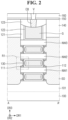
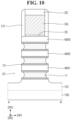
- a semiconductor device will be described below with reference to FIGS. 1 , 2 , 3 and 4 .
- FIG. 1 is a schematic layout diagram for explaining a semiconductor device according to one or more example embodiments.
- FIG. 2 is a cross-sectional view taken along line A-A' of FIG. 1 , according to one or more example embodiments.
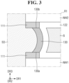
- FIG. 3 is an enlarged view of a region R1 of FIG. 2 .
- FIG. 4 is a cross-sectional view taken along line B-B' of FIG. 1 , according to one or more example embodiments.
- the semiconductor device includes a substrate 100, an active pattern 101, a field insulating layer 105, a plurality of nanosheets NW1, NW2 and NW3, a gate electrode G, a first barrier layer 111, a second barrier layer 112, a gate spacer 121, a gate insulating layer 122, a capping pattern 123, a first inner spacer 130, a source/drain region SD, a first interlayer insulating layer 140, a gate contact CB, an etching stop layer 150, a second interlayer insulating layer 160, and a via V.
- the substrate 100 may be a silicon substrate or silicon-on-insulator (SOI).
- SOI silicon-on-insulator
- the substrate 100 may include silicon germanium, silicon germanium on insulator (SGOI), indium antimonide, lead telluride, indium arsenide, indium phosphide, gallium arsenide or gallium antimonide, embodiments of the present disclosure are not limited to thereto.
- each of a first horizontal direction DR1 and a second horizontal direction DR2 may be defined as a direction parallel to an upper side of the substrate 100.
- the second horizontal direction DR2 may be defined as a direction different from the first horizontal direction DR1.
- a vertical direction DR3 may be defined as a direction perpendicular to each of the first horizontal direction DR1 and the second horizontal direction DR2. That is, the vertical direction DR3 may be defined as a direction perpendicular to the upper side of the substrate 100.
- the active pattern 101 may extend on the substrate 100 in the first horizontal direction DR1.
- the active pattern 101 may protrude from the upper side of the substrate 100 in the vertical direction DR3.
- the active pattern 101 may be a part of the substrate 100, and may include an epitaxial layer grown from the substrate 100.
- the field insulating layer 105 may be provided on the upper side of the substrate 100.
- the field insulating layer 105 may surround side walls of the active pattern 101.
- an upper surface of the active pattern 101 may protrude in the vertical direction DR3 beyond an upper surface of the field insulating layer 105.
- embodiment s the present disclosure are not limited thereto.
- the upper surface of the active pattern 101 may be provided on the same plane as the upper surface of the field insulating layer 105.
- the field insulating layer 105 may include, for example, an oxide film, a nitride film, an oxynitride film or a combination thereof.
- a plurality of nanosheets NW1, NW2 and NW3 may be provided on the active pattern 101.
- the plurality of nanosheets NW1, NW2 and NW3 may be stacked on the active pattern 101 to be spaced apart from each other in the vertical direction DR3.
- the plurality of nanosheets NW1, NW2 and NW3 may include a first nanosheet NW1, a second nanosheet NW2, and a third nanosheet NW3.
- the first nanosheet NW1 may be spaced apart from the active pattern 101 in the vertical direction DR3.
- the second nanosheet NW2 may be spaced apart from the first nanosheet NW1 in the vertical direction DR3.
- the third nanosheet NW3 may be spaced apart from the second nanosheet NW2 in the vertical direction DR3.
- FIGS. 2 and 4 show that the plurality of nanosheets NW1, NW2 and NW3 include three nanosheets spaced apart from each other in the vertical direction DR3, this is for convenience of explanation, and embodiments of the present disclosure are not limited thereto.
- the plurality of nanosheets may include four or more nanosheets spaced apart from each other and stacked in the vertical direction DR3.
- each of the first, second and third nanosheets NW1, NW2 and NW3 may include silicon (Si).
- Si silicon
- each of the first through third nanosheets NW1, NW2 and NW3 may include silicon germanium (SiGe).
- the gate electrode G may extend in the second horizontal direction DR2 on the active pattern 101 and the field insulating layer 105.
- the gate electrode G may surround each of the first, second and third nanosheets NW1, NW2 and NW3.
- the gate electrode G may include, for example, at least one of titanium nitride (TiN), tantalum carbide (TaC), tantalum nitride (TaN), titanium silicon nitride (TiSiN), tantalum silicon nitride (TaSiN), tantalum titanium nitride (TaTiN), titanium aluminum nitride (TiAlN), tantalum aluminum nitride (TaAlN), tungsten nitride (WN), ruthenium (Ru), titanium aluminum (TiAl), titanium aluminum carbonitride (TiAlC-N), titanium aluminum carbide (TiAlC), titanium carbide (TiC), tantalum carbonitride (TaCN),
- the gate spacer 121 may extend in the second horizontal direction DR2 along both side walls of the gate electrode G on the upper surfaces of the uppermost nanosheets of the plurality of nanosheets NW1, NW2 and NW3 and the field insulating layer 105.
- the gate spacer 121 may extend in the second horizontal direction DR2 along both side walls of the gate electrode G on the upper surface of the third nanosheet NW3 and the field insulating layer 105.
- the gate spacer 121 may include, for example, at least one of silicon nitride (SiN), silicon oxynitride (SiON), silicon oxide (SiO 2 ), silicon oxycarbonitride (SiOCN), silicon boronitride (SiBN), silicon oxyboronitride (SiOBN), silicon oxycarbide (SiOC), and combinations thereof.
- SiN silicon nitride
- SiON silicon oxide
- SiO 2 silicon oxide
- SiOCN silicon oxycarbonitride
- SiBN silicon boronitride
- SiOBN silicon oxyboronitride
- SiOC silicon oxycarbide
- the source/drain region SD may be provided on both sides of the gate electrode G on the active pattern 101.
- the source/drain region SD may be in contact with both side walls in the first horizontal direction DR1 of each of the plurality of nanosheets NW1, NW2 and NW3.
- the first inner spacer 130 may be provided on both side walls of the gate electrode G in the first horizontal direction DR1 between each of the plurality of nanosheets NW1, NW2 and NW3.
- the first inner spacer 130 may be provided on both side walls of the gate electrode G in the first horizontal direction DR1 between the first nanosheet NW1 and the second nanosheet NW2.
- the first inner spacer 130 may be provided on both side walls of the gate electrode G in the first horizontal direction DR1 between the second nanosheet NW2 and the third nanosheet NW3.
- the first inner spacer 130 may be provided on both side walls of the gate electrode G in the first horizontal direction DR1 between the active pattern 101 and the first nanosheet NW 1.
- the first inner spacer 130 may be provided between the gate electrode G and the source/drain region SD.
- the first inner spacers 130 may be in contact with the source/drain region SD.
- the side walls of the first inner spacers 130 that are in contact with the source/drain regions SD may be recessed toward the gate electrode G beyond the side walls of each of the plurality of nanosheets NW1, NW2 and NW3.
- the first inner spacer 130 may be spaced apart from the active pattern 101 and each of the plurality of nanosheets NW1, NW2 and NW3 in the vertical direction DR3.
- the first inner spacer 130 provided between the upper surface of the active pattern 101 and the lower surface of the first nanosheet NW1 may be spaced apart from each of the active pattern 101 and the first nanosheet NW1 in the vertical direction DR3.
- the first inner spacer 130 provided between the upper surface of the first nanosheet NW1 and the lower surface of the second nanosheet NW2 may be spaced apart from each of the first nanosheet NW1 and the second nanosheet NW2 in the vertical direction DR3.
- the first inner spacer 130 provided between the upper surface of the second nanosheet NW2 and the lower surface of the third nanosheet NW3 may be spaced apart from each of the second nanosheet NW2 and the third nanosheet NW3 in the third direction DR3.
- the first inner spacer 130 may include, for example, at least one of silicon nitride (SiN), silicon oxynitride (SiON), silicon oxide (SiO 2 ), silicon oxycarbonitride (SiOCN), silicon boronitride (SiBN), silicon oxyboronitride (SiOBN), silicon oxycarbide (SiOC), and combinations thereof.
- silicon nitride SiN
- silicon oxynitride SiON
- silicon oxide SiO 2
- SiOCN silicon oxycarbonitride
- SiBN silicon boronitride
- SiOBN silicon oxyboronitride
- SiOC silicon oxycarbide
- the first barrier layer 111 may be provided on a first side of the gate electrode G in the first horizontal direction DR1 between each of the plurality of nanosheets NW1, NW2 and NW3.
- the first barrier layer 111 may be provided on the first side of the gate electrode G in the first horizontal direction DR1 between the first nanosheet NW1 and the second nanosheet NW2.
- the first barrier layer 111 may be provided on the first side of the gate electrode G in the first horizontal direction DR1 between the second nanosheet NW2 and the third nanosheet NW3.
- the first barrier layer 111 may be provided on the first side of the gate electrode G in the first horizontal direction DR1 between the active pattern 101 and the first nanosheet NW1.
- the first barrier layer 111 may be in contact with each of the upper surface of the active pattern 101, the lower and upper surfaces of the first nanosheet NW1, the lower and upper surfaces of the second nanosheet NW2, and the lower surface of the third nanosheet NW3.
- the first barrier layer 111 may be provided between the upper surface of the active pattern 101 and the first inner spacer 130.
- the first barrier layer 111 may be provided between the lower surface of the first nanosheet NW1 and the first inner spacer 130.
- the first barrier layer 111 may be provided between the upper surface of the first nanosheet NW1 and the first inner spacer 130.
- the first barrier layer 111 may be provided between the lower surface of the second nanosheet NW2 and the first inner spacer 130.
- the first barrier layer 111 may be provided between the upper surface of the second nanosheet NW2 and the first inner spacer 130.
- the first barrier layer 111 may be provided between the lower surface of the third nanosheet NW3 and the first inner spacer 130.
- the first barrier layer 111 that is in contact with the upper surface of the active pattern 101 may be spaced apart in the vertical direction DR3 from the first barrier layer 111 that is in contact with the lower surface of the first nanosheet NW 1.
- the first barrier layer 111 that is in contact with the upper surface of the first nanosheet NW1 may be spaced apart in the vertical direction DR3 from the first barrier layer 111 that is in contact with the lower surface of the second nanosheet NW2.
- the first barrier layer 111 that is in contact with the upper surface of the second nanosheet NW2 may be spaced apart in the vertical direction DR3 from the first barrier layer 111 that is in contact with the lower surface of the third nanosheet NW3.
- each of the lower surface 130a and the upper surface 130b of the first inner spacer 130 may be in contact with the first barrier layer 111.
- each of the lower surface 130a and the upper surface 130b of the first inner spacer 130 may be in contact with the first barrier layer 111.
- each of the lower surface 130a and the upper surface 130b of the first inner spacer 130 may be in contact with the first barrier layer 111.
- the side walls of the first inner spacer 130 facing the gate electrode G may further protrude toward the gate electrode G beyond the side walls of the first barrier layer 111 facing the gate electrode G.
- the first barrier layer 111 may be in contact with the source/drain region SD.
- the side walls of the first barrier layer 111 that are in contact with the source/drain region SD may have an inclined profile that is continuous with the side walls of the plurality of nanosheets NW1, NW2 and NW3 in the first horizontal direction DR1.
- the first barrier layer 111 may include impurity-doped silicon (Si).
- impurities doped in the first barrier layer 111 may include at least one of germanium (Ge), arsenic (As), phosphorus (P), and nitrogen (N).
- the second barrier layer 112 may be provided on the second side of the gate electrode G opposite to the first side of the gate electrode G in the first horizontal direction DR1, between each of the plurality of nanosheets NW1, NW2 and NW3.
- the second barrier layer 112 may be provided on the second side of the gate electrode G in the first horizontal direction DR1, between the first nanosheet NW1 and the second nanosheet NW2.
- the second barrier layer 112 may be provided on the second side of the gate electrode G in the first horizontal direction DR1, between the second nanosheet NW2 and the third nanosheet NW3.
- the second barrier layer 112 may be provided on the second side of the gate electrode G in the first horizontal direction DR1, between the active pattern 101 and the first nanosheet NW1.
- the second barrier layer 112 may be spaced apart from the first barrier layer 111 in the first horizontal direction DR1.
- the second barrier layer 112 may be provided symmetrically with respect to the first barrier layer 111 relative to the gate electrode G.
- the second barrier layer 112 may include the same material as the first barrier layer 111.
- the second barrier layer 112 may include impurity-doped silicon (Si).
- impurities doped in the second barrier layer 112 may include at least one of germanium (Ge), arsenic (As), phosphorus (P), and nitrogen (N).
- the gate insulating layer 122 may be provided between the gate electrode G and the gate spacer 121.
- the gate insulating layer 122 may be provided between the gate electrode G and the active pattern 101.
- the gate insulating layer 122 may be provided between the gate electrode G and the field insulating layer 105.
- the gate insulating layer 122 may be provided between the gate electrode G and each of the plurality of nanosheets NW1, NW2 and NW3.
- the gate insulating layer 122 may be provided between the gate electrode G and the first inner spacer 130.
- the gate insulating layer 122 may be provided between the first barrier layer 111 and the second barrier layer 112. For example, at least a part of the gate insulating layer 122 may be provided between the first barrier layer 111 and the second barrier layer 112.
- the gate insulating layer 122 may be in contact with each of the side walls of the first barrier layer 111, the side walls of the second barrier layer 112, and the side walls of the inner spacer 130.
- the gate insulating layer 122 may include at least one of silicon oxide, silicon oxynitride, silicon nitride or a high dielectric constant material having a dielectric constant higher than silicon oxide.
- the high dielectric constant material may include, for example, one or more of hafnium oxide, hafnium silicon oxide, hafnium aluminum oxide, lanthanum oxide, lanthanum aluminum oxide, zirconium oxide, zirconium silicon oxide, tantalum oxide, titanium oxide, barium strontium titanium oxide, barium titanium oxide, strontium titanium oxide, yttrium oxide, aluminum oxide, lead scandium tantalum oxide or lead zinc niobate.
- a semiconductor device may include an NC (Negative Capacitance) FET that uses a negative capacitor.
- the gate insulating layer 122 may include a ferroelectric material film having ferroelectric properties, and a paraelectric material film having paraelectric properties.
- the ferroelectric material film may have a negative capacitance, and the paraelectric material film may have a positive capacitance.
- the overall capacitances decrease from the capacitance of each of the individual capacitors.
- the overall capacitances may be greater than an absolute value of each of the individual capacitances, while having a positive value.
- the overall capacitance values of the ferroelectric material film and the paraelectric material film connected in series may increase.
- a transistor including the ferroelectric material film may have a subthreshold swing (SS) below 60 mV/decade at room temperature.
- the ferroelectric material film may have ferroelectric properties.
- the ferroelectric material film may include, for example, at least one of hafnium oxide, hafnium zirconium oxide, barium strontium titanium oxide, barium titanium oxide, and lead zirconium titanium oxide.
- the hafnium zirconium oxide may be a material obtained by doping hafnium oxide with zirconium (Zr).
- the hafnium zirconium oxide may be a compound of hafnium (Hf), zirconium (Zr), and oxygen (O).
- the ferroelectric material film may further include a doped dopant.
- the dopant may include at least one of aluminum (Al), titanium (Ti), niobium (Nb), lanthanum (La), yttrium (Y), magnesium (Mg), silicon (Si), calcium (Ca), cerium (Ce), dysprosium (Dy), erbium (Er), gadolinium (Gd), germanium (Ge), scandium (Sc), strontium (Sr), and tin (Sn).
- the type of dopant included in the ferroelectric material film may vary, depending on which type of ferroelectric material is included in the ferroelectric material film.
- the dopant included in the ferroelectric material film may include, for example, at least one of gadolinium (Gd), silicon (Si), zirconium (Zr), aluminum (Al), and yttrium (Y).
- Gd gadolinium
- Si silicon
- Zr zirconium
- Al aluminum
- Y yttrium
- the ferroelectric material film may include 3 to 8 at% (atomic %) aluminum.
- a ratio of the dopant may be a ratio of aluminum to the sum of hafnium and aluminum.
- the ferroelectric material film may include 2 to 10 at% silicon.
- the dopant is yttrium (Y)
- the ferroelectric material film may include 2 to 10 at% yttrium.
- the dopant is gadolinium (Gd)
- the ferroelectric material film may include 1 to 7 at% gadolinium.
- the dopant is zirconium (Zr)
- the ferroelectric material film may include 50 to 80 at% zirconium.
- the paraelectric material film may have the paraelectric properties.
- the paraelectric material film may include at least one of, for example, a silicon oxide and a metal oxide having a high dielectric constant.
- the metal oxide included in the paraelectric material film may include, for example, but is not limited to, at least one of hafnium oxide, zirconium oxide, and aluminum oxide.
- the ferroelectric material film and the paraelectric material film may include the same material.
- the ferroelectric material film may have ferroelectric properties, but the paraelectric material film may not have ferroelectric properties.
- the ferroelectric material film and the paraelectric material film include hafnium oxide
- a crystal structure of hafnium oxide included in the ferroelectric material film may be different from a crystal structure of hafnium oxide included in the paraelectric material film.
- the ferroelectric material film may have a thickness having ferroelectric properties.
- a thickness of the ferroelectric material film may be, for example, but is not limited to, 0.5 to 10 nm. Because a critical thickness that exhibits ferroelectric properties may vary for each ferroelectric material, the thickness of the ferroelectric material film may vary depending on the ferroelectric material.
- the gate insulating layer 122 may include one ferroelectric material film.
- the gate insulating layer 122 may include a plurality of ferroelectric material films spaced apart from each other.
- the gate insulating layer 122 may have a stacked film structure in which the plurality of ferroelectric material films and the plurality of paraelectric material films are alternately stacked.
- the capping pattern 123 may extend in the second horizontal direction DR2 on each of the gate spacer 121, the gate insulating layer 122 and the gate electrode G.
- the capping pattern 123 may be in contact with the upper surface of the gate spacer 121.
- the capping pattern 123 may be provided between the gate spacers 121.
- the capping pattern 123 may include, for example, at least one of silicon nitride (SiN), silicon oxynitride (SiON), silicon oxide (SiO 2 ), silicon carbonitride (SiCN), silicon oxycarbonitride (SiOCN), and combinations thereof.
- SiN silicon nitride
- SiON silicon oxide
- SiO 2 silicon carbonitride
- SiOCN silicon oxycarbonitride
- a first interlayer insulating layer 140 may be provided on the field insulating layer 105.
- the first interlayer insulating layer 140 may cover the source/drain region SD.
- the first interlayer insulating layer 140 may surround side walls of each of the gate spacer 121 and the capping pattern 123.
- the upper surface of the first interlayer insulating layer 140 may be provided on the same plane as the upper surface of the capping pattern 123.
- embodiments of the present disclosure are not limited thereto.
- the first interlayer insulating layer 140 may cover the upper surface of the capping pattern 123.
- the first interlayer insulating layer 140 may include, for example, at least one of silicon oxide, silicon nitride, silicon oxynitride, and a low dielectric constant material.
- the low dielectric constant material may include, for example, Fluorinated TetraEthylOrthoSilicate (FTEOS), Hydrogen SilsesQuioxane (HSQ), Bis-benzoCycloButene (BCB), TetraMethylOrthoSilicate (TMOS), OctaMethyleyCloTetraSiloxane (OMCTS), HexaMethylDiSiloxane (HMDS), TriMethylSilyl Borate (TMSB), DiAcetoxyDitertiaryButoSiloxane (DADBS), TriMethylSilil Phosphate (TMSP), PolyTetraFluoroEthylene (PTFE), TOSZ (Tonen SilaZen), FSG (Flu
- the gate contact CB may penetrate the capping pattern 123 in the vertical direction DR3 and may be connected to the gate electrode G.
- the upper surface of the gate contact CB may be provided on the same plane as the upper surface of the first interlayer insulating layer 140.
- FIGS. 2 and 4 show that the gate contact CB is formed of a single film, embodiments of the present disclosure are not limited thereto. In one or more example embodiments, the gate contact CB may be formed of multiple films.
- the gate contact CB may include, for example, at least one of tantalum (Ta), tantalum nitride (TaN), titanium (Ti), titanium nitride (TiN), ruthenium (Ru), cobalt (Co), nickel (Ni), nickel boron (NiB), tungsten (W), tungsten nitride (WN), zirconium (Zr), zirconium nitride (ZrN), vanadium (V), vanadium nitride (VN), niobium (Nb), niobium nitride (NbN), platinum (Pt), iridium (Ir), rhodium (Rh), aluminum (Al), copper (Cu) and molybdenum (Mo).
- Ta tantalum
- TaN tantalum nitride
- Ti titanium
- TiN titanium nitride
- Ru ruthenium
- cobalt Co
- nickel nickel
- NiB nickel
- the etching stop layer 150 may be provided on upper surfaces of each of the first interlayer insulating layer 140, the capping pattern 123, and the gate contact CB. Although FIGS. 2 and 4 show that the etching stop layer 150 is formed of a single film, embodiments of the present disclosure are not limited thereto. In one or more example embodiments, the etching stop layer 150 may be formed of multiple films.
- the etching stop layer 150 may include, for example, at least one of aluminum oxide, aluminum nitride, hafnium oxide, zirconium oxide, silicon oxide, silicon nitride, silicon oxynitride, and a low dielectric constant material.
- a second interlayer insulating layer 160 may be provided on the etching stop layer 150.
- the second interlayer insulating layer 160 may include, for example, at least one of silicon oxide, silicon nitride, silicon oxynitride, and a low dielectric constant material.
- the via V may penetrate the second interlayer insulating layer 160 and the etching stop layer 150 in the vertical direction DR3 and may be connected to the gate contact CB.
- FIGS. 2 and 4 show that the via V is formed of a single film, embodiments of the present disclosure are not limited thereto. In one or more example embodiments, the via V may be formed of multiple films.
- the via V may include a conductive material.
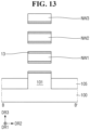
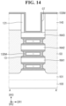
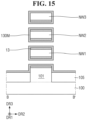
- a method for fabricating a semiconductor device according to one or more example embodiments will be described below with reference to FIGS. 2 , 3 , 4 , 5 , 6 , 7 , 8 , 9 , 10 , 11 , 12 , 13 , 14 , 15 , 16 , 17 , 18 , 19 , 20 and 21 .
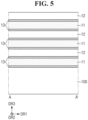
- FIGS. 5 , 6 , 7 , 8 , 9 , 10 , 11 , 12 , 13 , 14 , 15 , 16 , 17 , 18 , 19 , 20 and 21 are intermediate step diagrams for explaining the method for fabricating the semiconductor device according to one or more example embodiments.
- a stacked structure may be provided on the substrate 100.
- the stacked structure may include a sacrificial layer 11, a semiconductor layer 12 and a barrier material layer 13.
- the sacrificial layer 11 and the semiconductor layer 12 may be alternately stacked on the substrate 100.
- the barrier material layer 13 may be provided between the substrate 100 and the lowermost sacrificial layer 11, and between the sacrificial layer 11 and the semiconductor layer 12, respectively.
- the barrier material layer 13 may be provided at the lowermost part of the stacked structure, and the semiconductor layer 12 may be provided at the uppermost part of the stacked structure.
- the sacrificial layer 11 may include silicon germanium (SiGe)
- the semiconductor layer 12 may include silicon (Si)
- the barrier material layer 13 may include impurity-doped silicon (Si).
- the impurities doped in the barrier material layer 13 may include at least one of germanium (Ge), arsenic (As), phosphorus (P) and nitrogen (N).
- embodiments are not limited to the aforementioned configurations.
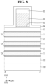
- a part of the stacked structure may be etched. That is, a part of each of the sacrificial layer 11, the semiconductor layer 12 and the barrier material layer 13 may be etched. A part of the substrate 100 may also be etched, while the stacked structure is being etched. An active pattern 101 may be provided below the stacked structure on the substrate 100 through such an etching process. That is, the active pattern 101 may be provided below the lowermost barrier material layer 13. The active pattern 101 may extend in the first horizontal direction DR1.
- the field insulating layer 105 may then be provided on the substrate 100.
- the field insulating layer 105 may surround side walls of the active pattern 101.
- the upper surface of the active pattern 101 may be provided to be higher than the upper surface of the field insulating layer 105.
- a pad oxide layer 20 may be provided to cover the upper surface of the field insulating layer 105, the side walls of each of the exposed active patterns 101, and the side walls and upper surface of the stacked structure.
- the pad oxide layer 20 may be provided conformally.
- the pad oxide layer 20 may include, for example, silicon oxide (SiO 2 ).
- a dummy gate DG and a dummy capping pattern DC extending in the second horizontal direction DR2 may be provided on the pad oxide layer 20 on the stack structure and the field insulating layer 105.
- the dummy capping pattern DC may be provided on the dummy gate DG. While the dummy gate DG and the dummy capping pattern DC are being provided, the remaining pad oxide layer 20 on the substrate 100 except for the portion that overlaps the dummy gate DG in the vertical direction DR3 may be removed.
- a spacer material layer SM may be provided to cover the side walls of the dummy gate DG, the side walls and upper surface of each of the dummy capping patterns DC, the side walls and upper surface of the exposed stacked structure, and the upper surface of the field insulating layer 105.
- the spacer material layer SM may be provided conformally.
- the spacer material layer SM may include, for example, at least one of silicon nitride (SiN), silicon oxycarbonitride (SiOCN), silicon boron carbonitride (SiBCN), silicon carbonitride (SiCN), silicon oxynitride (SiON), and combinations thereof.
- a source/drain trench ST may be provided by etching the stacked structure, using the dummy gate DG and the dummy capping pattern DC as masks.
- the source/drain trench ST may extend into the active pattern 101.
- a part of each of the spacer material layer (SM of FIG. 8 ) provided on the upper surface of the dummy capping pattern DC, and the dummy capping pattern DC may be etched.
- a part of both side walls of the sacrificial layer 11 in the first horizontal direction DR1 may be etched during the formation of the source/drain trench ST. Accordingly, both side walls of the sacrificial layer 11 in the first horizontal direction DR1 may be recessed toward the center.
- a spacer material layer (SM of FIG. 8 ) that remains on side walls of the dummy capping pattern DC and the dummy gate DG may be provided as the gate spacer 121.
- each of the semiconductor layers (12 of FIG. 8 ) that remains below the dummy gate DG on the active pattern 101 may be provided as first, second and third nanosheets NW1, NW2 and NW3.
- the source/drain region SD may be provided inside the source/drain trench (ST of FIG. 10 ).
- the source/drain region SD may be epitaxially grown from each of the active pattern 101, the sacrificial layer 11, the barrier material layer 13, and the first, second and third nanosheets NW1, NW2 and NW3.
- the first interlayer insulating layer 140 may be provided to cover each of the source/drain region SD, the gate spacer 121, and the dummy capping pattern DC.
- the upper surface of the dummy gate (DG of FIG. 11 ) may be exposed through a planarization process. Subsequently, each of the dummy gate (DG of FIG. 11 ), the pad oxide layer (20 of FIG. 11 ) and the sacrificial layer (11 of FIG. 11 ) may be etched. A portion from which the dummy gate (DG of FIG. 11 ) is removed may be provided as a gate trench GT.
- an inner spacer material layer 130M may be provided in the etched portions of each of the dummy gate (DG of FIG. 11 ), the pad oxide layer (20 of FIG. 11 ) and the sacrificial layer (11 of FIG. 11 ).
- the inner spacer material layer 130M may be provided along each of the surface of the exposed source/drain region SD, the surface of the exposed barrier material layer 13, the surface of the exposed active pattern 101, the surface of the exposed field insulating layer 105, and the surfaces of each of the exposed first, second and third nanosheets NW1, NW2 and NW3.
- the inner spacer material layer 130M may also be provided on the surface of the exposed gate spacer 121 and the upper surface of the first interlayer insulating layer 140.
- the inner spacer material layer 130M provided on the surface of the exposed source/drain region SD may be thicker than the inner spacer material layer 130M provided at other portions.
- a cavity surrounded by the inner spacer material layer 130M may be provided between the active pattern 101 and each of the first, second and third nanosheets NW1, NW2 and NW3.
- the inner spacer material layer 130M may include, for example, at least one of silicon nitride (SiN), silicon oxynitride (SiON), silicon oxide (SiO 2 ), silicon oxycarbonitride (SiOCN), silicon boronitride (SiBN), silicon oxyboronitride (SiOBN), silicon oxycarbide (SiOC), and combinations thereof.
- SiN silicon nitride
- SiON silicon oxide
- SiO 2 silicon oxide
- SiOCN silicon oxycarbonitride
- SiBN silicon boronitride
- SiOBN silicon oxyboronitride
- SiOC silicon oxycarbide
- a part of the inner spacer material layer (130M of FIGS. 14 and 15 ) may be etched.
- the remaining inner spacer material layer (130M of FIGS. 14 and 15 ) except for the portion that is in contact with the source/drain regions SD may be etched.
- the inner spacer material layer (130M of FIGS. 14 and 15 ) that remains in the portion that is in contact with the source/drain regions SD may be provided as a first inner spacer 130.
- the first inner spacer 130 may be selectively provided only in the portion that is in contact with the source/drain regions SD.
- a part of the exposed barrier material layer (13 of FIGS. 16 and 17 ) may be etched. While the etching process is performed on the barrier material layer (13 of FIGS. 16 and 17 ), the remaining material layer other than the barrier material layer (13 of FIGS. 16 and 17 ) that exists on the lower and upper surfaces of the first inner spacer 130 may be etched. As a result, some of the upper surface of the active pattern 101 and the lower and upper surfaces of each of the first, second and third nanosheets NW1, NW2 and NW3 may be exposed. After the etching process is performed on the barrier material layer (13 of FIGS. 16 and 17 ), the remaining barrier material layer (13 of FIGS. 16 and 17 ) may be provided as a first barrier layer 111 and a second barrier layer 112. The second barrier layer 112 may be spaced apart from the first barrier layer 111 in the first horizontal direction DR1.
- the gate insulating layer 122 may be provided along the surface of the exposed first inner spacer 130, the surface of the exposed first barrier layer 111, the surface of the exposed second barrier layer 112, the surface of the exposed active pattern 101, the surface of the exposed field insulating layer 105, and the surfaces of each of the exposed first, second and third nanosheets NW 1, NW2 and NW3.
- the gate insulating layer 122 may also be provided on the side walls of the gate trench (GT of FIG. 18 ).
- a gate electrode G may be provided on the gate insulating layer 122. Subsequently, a part of each of the upper part of each of the gate spacer 121, the gate insulating layer 122, and the gate electrode G may be etched. Next, the capping pattern 123 may be provided on the etched portions of each of the gate spacer 121, the gate insulating layer 122, and the gate electrode G.
- a gate contact CB penetrating the capping pattern 123 in the vertical direction DR3 and connected to the gate electrode G may be provided.
- an etching stop layer 150 and a second interlayer insulating layer 160 may be sequentially provided on the first interlayer insulating layer 140, the capping pattern 123, and the gate contact CB.
- a via V which penetrates the etching stop layer 150 and the second interlayer insulating layer 160 in the vertical direction DR3 and is connected to the gate contact CB may be provided.
- the semiconductor device shown in FIGS. 2 , 3 and 4 may be fabricated.
- the inner spacer 130 may be provided on a side wall of the source/drain region SD after the dummy gate DG is removed. That is, in the semiconductor device according to one or more example embodiments, the inner spacer 130 may be provided on side walls of the source/drain region SD, after the source/drain region SD is provided.
- the barrier material layer 13 (provided as the first barrier layer 111 and the second barrier layer 112 through a subsequent process) is provided on the surfaces of the plurality of nanosheets NW1, NW2 and NW3 of the portion in which the inner spacer 130 is provided, and the inner spacer 130 may be provided on the side walls of the exposed source/drain region SD in a subsequent process.
- the barrier material layer 13 (provided as the first barrier layer 111 and the second barrier layer 112 through a subsequent process) may suppress the inner spacer 130 from being provided on the surfaces of the exposed plurality of nanosheets NW1, NW2 and NW3 in the process of forming the inner spacer 130.
- the inner spacer 130 may be selectively provided on the side walls of exposed the source/drain region SD through such a process. Therefore, the semiconductor device according to one or more example embodiments can improve reliability on each of the source/drain region SD and the inner spacer 130.
- the first barrier layer 111 and the second barrier layer 112 may be provided between the inner spacer 130 and the plurality of nanosheets NW1, NW2 and NW3. That is, the inner spacer 130 may be spaced apart from each of the plurality of nanosheets NW1, NW2 and NW3 in the vertical direction DR3.
- FIGS. 22 and 23 a semiconductor device according to one or more example embodiments will be described with reference to FIGS. 22 and 23 .
- the description will focus on differences from the semiconductor device shown in FIGS. 1 , 2 , 3 and 4 .
- FIG. 22 is a cross-sectional view for explaining the semiconductor device according to one or more example embodiments.
- FIG. 23 is an enlarged view of a region R2 of FIG. 22 , according to one or more example embodiments.
- At least a part of a gate insulating layer 222 may abut each of the lower surface 130a and the upper surface 130b of the first inner spacer 130.
- each of the side walls of the first barrier layer 211 and the side walls of the second barrier layer 212 that are in contact with the gate insulating layer 222 may be recessed toward the source/drain region SD beyond the side walls of the first inner spacer 130 facing the gate electrode G. That is, each of the side walls of the first barrier layer 211 and the side walls of the second barrier layer 212 that abut the gate insulating layer 222 may be located on each of the lower surface 130a and the upper surface 130b of the first inner spacer 130.
- At least a part of the gate insulating layer 222 may be in contact with each of the lower surface 130a and the upper surface 130b of the first inner spacer 130, on each of the side walls of the first barrier layer 211 and the side walls of the second barrier layer 212 recessed toward the source/drain region SD.
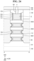
- FIG. 24 a semiconductor device according to one or more example embodiments will be described with reference to FIG. 24 .
- the description will focus on differences from the semiconductor device according to one or more example embodiments shown in FIGS. 1 , 2 , 3 and 4 .
- FIG. 24 is a cross-sectional view for explaining a semiconductor device according to one or more example embodiments.
- a second inner spacer 331 may be provided between the gate spacer 121 and the gate insulating layer 322.
- a part of the inner spacer material layer 130M of FIG. 14
- an upper surface of the second inner spacer 331 may be in contact with the capping pattern 123.
- the second inner spacer 331 may be in contact with the upper surface of the third nanosheet NW3.
- the second inner spacer 331 may include the same material as that of the first inner spacer 130.
- the second inner spacer 331 may include, for example, at least one of silicon nitride (SiN), silicon oxynitride (SiON), silicon oxide (SiO 2 ), silicon oxycarbonitride (SiOCN), silicon boronitride (SiBN), silicon oxyboronitride (SiOBN), silicon oxycarbide (SiOC), and combinations thereof.
- silicon nitride SiN
- silicon oxynitride SiON
- silicon oxide SiO 2
- silicon oxycarbonitride SiOCN
- silicon boronitride SiBN
- SiOBN silicon oxyboronitride
- SiOC silicon oxycarbide
Landscapes
- Insulated Gate Type Field-Effect Transistor (AREA)
Applications Claiming Priority (1)
| Application Number | Priority Date | Filing Date | Title |
|---|---|---|---|
| KR1020230067326A KR20240169740A (ko) | 2023-05-25 | 2023-05-25 | 반도체 장치 |
Publications (1)
| Publication Number | Publication Date |
|---|---|
| EP4468363A1 true EP4468363A1 (de) | 2024-11-27 |
Family
ID=89620150
Family Applications (1)
| Application Number | Title | Priority Date | Filing Date |
|---|---|---|---|
| EP24152165.7A Pending EP4468363A1 (de) | 2023-05-25 | 2024-01-16 | Halbleiteranordnung |
Country Status (4)
| Country | Link |
|---|---|
| US (1) | US20240395887A1 (de) |
| EP (1) | EP4468363A1 (de) |
| JP (1) | JP2024169353A (de) |
| KR (1) | KR20240169740A (de) |
Cited By (1)
| Publication number | Priority date | Publication date | Assignee | Title |
|---|---|---|---|---|
| EP4550973A1 (de) * | 2023-11-01 | 2025-05-07 | Samsung Electronics Co., Ltd. | Halbleiteranordnung |
Families Citing this family (1)
| Publication number | Priority date | Publication date | Assignee | Title |
|---|---|---|---|---|
| US20250063781A1 (en) * | 2023-08-18 | 2025-02-20 | Taiwan Semiconductor Manufacturing Company, Ltd. | Semiconductor structure and method for forming the same |
Citations (5)
| Publication number | Priority date | Publication date | Assignee | Title |
|---|---|---|---|---|
| US20200411698A1 (en) * | 2019-06-25 | 2020-12-31 | Samsung Electronics Co., Ltd. | Semiconductor devices |
| US20210043727A1 (en) * | 2019-08-07 | 2021-02-11 | Globalfoundries Inc. | Gate-all-around field effect transistors with robust inner spacers and methods |
| US20220140081A1 (en) * | 2020-01-14 | 2022-05-05 | Samsung Electronics Co., Ltd. | Method of manufacturing a semiconductor device |
| US20220278195A1 (en) * | 2021-03-01 | 2022-09-01 | International Business Machines Corporation | Nanosheet metal-oxide semiconductor field effect transistor with asymmetric threshold voltage |
| US20230411454A1 (en) * | 2022-06-21 | 2023-12-21 | Samsung Electronics Co., Ltd. | Semiconductor device |
-
2023
- 2023-05-25 KR KR1020230067326A patent/KR20240169740A/ko active Pending
- 2023-12-14 US US18/540,389 patent/US20240395887A1/en active Pending
-
2024
- 2024-01-16 EP EP24152165.7A patent/EP4468363A1/de active Pending
- 2024-05-17 JP JP2024081259A patent/JP2024169353A/ja active Pending
Patent Citations (5)
| Publication number | Priority date | Publication date | Assignee | Title |
|---|---|---|---|---|
| US20200411698A1 (en) * | 2019-06-25 | 2020-12-31 | Samsung Electronics Co., Ltd. | Semiconductor devices |
| US20210043727A1 (en) * | 2019-08-07 | 2021-02-11 | Globalfoundries Inc. | Gate-all-around field effect transistors with robust inner spacers and methods |
| US20220140081A1 (en) * | 2020-01-14 | 2022-05-05 | Samsung Electronics Co., Ltd. | Method of manufacturing a semiconductor device |
| US20220278195A1 (en) * | 2021-03-01 | 2022-09-01 | International Business Machines Corporation | Nanosheet metal-oxide semiconductor field effect transistor with asymmetric threshold voltage |
| US20230411454A1 (en) * | 2022-06-21 | 2023-12-21 | Samsung Electronics Co., Ltd. | Semiconductor device |
Cited By (1)
| Publication number | Priority date | Publication date | Assignee | Title |
|---|---|---|---|---|
| EP4550973A1 (de) * | 2023-11-01 | 2025-05-07 | Samsung Electronics Co., Ltd. | Halbleiteranordnung |
Also Published As
| Publication number | Publication date |
|---|---|
| US20240395887A1 (en) | 2024-11-28 |
| KR20240169740A (ko) | 2024-12-03 |
| JP2024169353A (ja) | 2024-12-05 |
Similar Documents
| Publication | Publication Date | Title |
|---|---|---|
| KR102852242B1 (ko) | 반도체 장치 및 이의 제조 방법 | |
| KR102902014B1 (ko) | 반도체 장치 | |
| US11869938B2 (en) | Semiconductor device | |
| KR20220091756A (ko) | 반도체 장치 | |
| EP4468363A1 (de) | Halbleiteranordnung | |
| US12148749B2 (en) | Semiconductor device and method for fabricating the same | |
| KR20230174550A (ko) | 반도체 장치 | |
| US20240120400A1 (en) | Semiconductor device | |
| US12471332B2 (en) | Semiconductor device | |
| EP4550973A1 (de) | Halbleiteranordnung | |
| US20240413206A1 (en) | Semiconductor device with doped source/drain region | |
| US12501672B2 (en) | Semiconductor device | |
| US20230352523A1 (en) | Semiconductor device | |
| US20250089352A1 (en) | Semiconductor device | |
| US20240222468A1 (en) | Method for fabricating semiconductor device | |
| US20260068297A1 (en) | Semiconductor device comprising fin-shaped pattern | |
| US20240405113A1 (en) | Semiconductor device | |
| US20260129929A1 (en) | Semiconductor device | |
| US20260059850A1 (en) | Semiconductor device | |
| US20260114022A1 (en) | Semiconductor device and manufacturing methods of the same | |
| US20260047188A1 (en) | Semiconductor device | |
| US20260032995A1 (en) | Semiconductor devices | |
| US20240145560A1 (en) | Semiconductor device | |
| US20230402456A1 (en) | Semiconductor device | |
| US20250324712A1 (en) | Semiconductor device |
Legal Events
| Date | Code | Title | Description |
|---|---|---|---|
| PUAI | Public reference made under article 153(3) epc to a published international application that has entered the european phase |
Free format text: ORIGINAL CODE: 0009012 |
|
| STAA | Information on the status of an ep patent application or granted ep patent |
Free format text: STATUS: EXAMINATION IS IN PROGRESS |
|
| 17P | Request for examination filed |
Effective date: 20240116 |
|
| AK | Designated contracting states |
Kind code of ref document: A1 Designated state(s): AL AT BE BG CH CY CZ DE DK EE ES FI FR GB GR HR HU IE IS IT LI LT LU LV MC ME MK MT NL NO PL PT RO RS SE SI SK SM TR |
|
| P01 | Opt-out of the competence of the unified patent court (upc) registered |
Free format text: CASE NUMBER: APP_66295/2024 Effective date: 20241213 |