EP4468367A1 - Kondensator und herstellungsverfahren dafür - Google Patents
Kondensator und herstellungsverfahren dafür Download PDFInfo
- Publication number
- EP4468367A1 EP4468367A1 EP22938798.0A EP22938798A EP4468367A1 EP 4468367 A1 EP4468367 A1 EP 4468367A1 EP 22938798 A EP22938798 A EP 22938798A EP 4468367 A1 EP4468367 A1 EP 4468367A1
- Authority
- EP
- European Patent Office
- Prior art keywords
- electrode plate
- conductive part
- capacitor
- substrate
- dielectric layer
- Prior art date
- Legal status (The legal status is an assumption and is not a legal conclusion. Google has not performed a legal analysis and makes no representation as to the accuracy of the status listed.)
- Pending
Links
Images


Classifications
-
- H—ELECTRICITY
- H10—SEMICONDUCTOR DEVICES; ELECTRIC SOLID-STATE DEVICES NOT OTHERWISE PROVIDED FOR
- H10D—INORGANIC ELECTRIC SEMICONDUCTOR DEVICES
- H10D1/00—Resistors, capacitors or inductors
- H10D1/60—Capacitors
- H10D1/62—Capacitors having potential barriers
-
- H—ELECTRICITY
- H01—ELECTRIC ELEMENTS
- H01G—CAPACITORS; CAPACITORS, RECTIFIERS, DETECTORS, SWITCHING DEVICES, LIGHT-SENSITIVE OR TEMPERATURE-SENSITIVE DEVICES OF THE ELECTROLYTIC TYPE
- H01G4/00—Fixed capacitors; Processes of their manufacture
- H01G4/002—Details
- H01G4/005—Electrodes
- H01G4/012—Form of non-self-supporting electrodes
-
- H—ELECTRICITY
- H01—ELECTRIC ELEMENTS
- H01G—CAPACITORS; CAPACITORS, RECTIFIERS, DETECTORS, SWITCHING DEVICES, LIGHT-SENSITIVE OR TEMPERATURE-SENSITIVE DEVICES OF THE ELECTROLYTIC TYPE
- H01G4/00—Fixed capacitors; Processes of their manufacture
- H01G4/002—Details
- H01G4/228—Terminals
-
- H—ELECTRICITY
- H01—ELECTRIC ELEMENTS
- H01G—CAPACITORS; CAPACITORS, RECTIFIERS, DETECTORS, SWITCHING DEVICES, LIGHT-SENSITIVE OR TEMPERATURE-SENSITIVE DEVICES OF THE ELECTROLYTIC TYPE
- H01G4/00—Fixed capacitors; Processes of their manufacture
- H01G4/33—Thin- or thick-film capacitors (thin- or thick-film circuits; capacitors without a potential-jump or surface barrier specially adapted for integrated circuits, details thereof, multistep manufacturing processes therefor)
-
- H—ELECTRICITY
- H01—ELECTRIC ELEMENTS
- H01G—CAPACITORS; CAPACITORS, RECTIFIERS, DETECTORS, SWITCHING DEVICES, LIGHT-SENSITIVE OR TEMPERATURE-SENSITIVE DEVICES OF THE ELECTROLYTIC TYPE
- H01G4/00—Fixed capacitors; Processes of their manufacture
- H01G4/002—Details
- H01G4/005—Electrodes
-
- H—ELECTRICITY
- H10—SEMICONDUCTOR DEVICES; ELECTRIC SOLID-STATE DEVICES NOT OTHERWISE PROVIDED FOR
- H10W—GENERIC PACKAGES, INTERCONNECTIONS, CONNECTORS OR OTHER CONSTRUCTIONAL DETAILS OF DEVICES COVERED BY CLASS H10
- H10W20/00—Interconnections in chips, wafers or substrates
- H10W20/20—Interconnections within wafers or substrates, e.g. through-silicon vias [TSV]
Definitions
- the present disclosure relates to the capacitor field, and more specifically, to a capacitor having an ultra-low loss at a high frequency and a method for preparing the capacitor.
- a capacitor in a form of a metal-oxide-semiconductor field-effect transistor may be introduced at an input end to match input impedance, to maximize performance of the radio frequency device.
- Metal-Oxide-Semiconductor Field-Effect Transistor, MOSFET Metal-Oxide-Semiconductor Field-Effect Transistor
- Radio frequency losses of the capacitor at the input end are easily caused in a high-frequency operating condition due to a limitation of a physical characteristic of an electrode material of a substrate. As an operating frequency band of the capacitor increases, these radio frequency losses further increase. Therefore, how to reduce the radio frequency losses of the capacitor is a challenge for a designer.
- embodiments of the present disclosure relate to technical solutions for a capacitor, and specifically provide a capacitor and a method for preparing the capacitor, to reduce a loss of the capacitor at a high frequency.
- a capacitor includes: a substrate, having a first surface and a second surface opposite to the first surface, where the substrate is provided with a via that runs through the first surface to the second surface; a first electrode plate, coupled to the first surface of the substrate; a first conductive part, disposed on the second surface of the substrate; a second conductive part, disposed on a side that is of the first electrode plate and that faces the via; and a third conductive part, disposed on an inner wall of the via, to couple the first conductive part to the second conductive part.
- the first surface and the second surface of the substrate are short-circuited through the conductive parts.
- effective bypass effect can be formed for the substrate, so that a dielectric loss of the capacitor in a high-frequency operating condition can be significantly reduced, and performance of the capacitor can be improved.
- the first electrode plate includes a first part and a second part
- the capacitor further includes: a first dielectric layer, located on the first part of the first electrode plate and coupled to the first part, and a second electrode plate, located on the first dielectric layer and coupled to the first electrode plate through the first dielectric layer. In this way, it can be ensured that the capacitor operates stably.
- the capacitor further includes a second dielectric layer, located on the second part of the first electrode plate and at least a part of the second electrode plate. In this way, components of the capacitor can be protected from water and impact.
- the first dielectric layer includes at least one of the following materials: silicon nitride, silicon oxide, silicon oxynitride, silicon oxide, aluminum oxide, and titanium oxide. In this way, a plurality of materials can be used to prepare the first medium layer, so that preparation of the first medium layer is more flexible.
- the second electrode plate includes at least one of the following materials: gold, silver, aluminum, nickel, titanium, platinum, copper, tungsten, tin, tantalum, titanium nitride, tungsten silicide, and tantalum nitride. In this way, similarly, a plurality of materials can be used to prepare the second electrode plate, so that preparation of the second electrode plate is more flexible.
- the second dielectric layer includes at least one of the following materials: silicon nitride, silicon oxide, silicon oxynitride, silicon oxide, aluminum oxide, and titanium oxide. In this way, an appropriate material can be selected from various materials based on an actual design requirement, to prepare the second dielectric layer.
- the first conductive part, the second conductive part, and the third conductive part are integrally formed. In this way, the conductive parts can be formed conveniently and quickly.
- a cross section of the via is a circle, an ellipse, a long strip, or a polygon. In this way, an expected via can be obtained based on different design requirements.
- the first conductive part, the second conductive part, and the third conductive part include at least one of the following materials: nickel, titanium, aluminum, lead, platinum, gold, titanium nitride, tantalum nitride, and copper. In this way, short-circuiting effect of the first surface and the second surface of the substrate can be ensured through a conductive characteristic of the conductive part, to ensure performance of the capacitor.
- the first electrode plate includes at least one of the following materials: gold, silver, aluminum, nickel, titanium, platinum, copper, tungsten, tin, tantalum, titanium nitride, tungsten silicide, and tantalum nitride. In this way, an appropriate material can be flexibly selected from various materials based on an actual design requirement, to prepare the first electrode plate.
- a method for preparing a capacitor includes: providing a substrate, where the substrate has a first surface and a second surface opposite to the first surface; providing, on the substrate, a via that runs through the first surface to the second surface; providing a first electrode plate on the substrate, where the first electrode plate is coupled to the first surface of the substrate; providing a first conductive part on the second surface of the substrate; providing a second conductive part on a side that is of the first electrode plate and that faces the via; and providing a third conductive part on an inner wall of the via, to couple the first conductive part to the second conductive part.
- the first electrode plate includes a first part and a second part
- the method further includes: providing a dielectric material on the first electrode plate; and removing a part that is of the dielectric material and that is coupled to the second part, to form a first dielectric layer.
- the method further includes: providing a second electrode plate on the first dielectric layer, where the second electrode plate is coupled to the first electrode plate through the first dielectric layer.
- the method further includes: providing a wrapping material on the second part of the first electrode plate and the second electrode plate; and removing a part that is of the wrapping material and that is on the second electrode plate, to form a second dielectric layer.
- the first dielectric layer includes at least one of the following materials: silicon nitride, silicon oxide, silicon oxynitride, silicon oxide, aluminum oxide, and titanium oxide.
- the second electrode plate includes at least one of the following materials: gold, silver, aluminum, nickel, titanium, platinum, copper, tungsten, tin, tantalum, titanium nitride, tungsten silicide, and tantalum nitride.
- the second dielectric layer includes at least one of the following materials: silicon nitride, silicon oxide, silicon oxynitride, silicon oxide, aluminum oxide, and titanium oxide.
- the first conductive part, the second conductive part, and the third conductive part are integrally formed.
- a cross section of the via is a circle, an ellipse, a long strip, or a polygon.
- the first conductive part, the second conductive part, and the third conductive part include at least one of the following materials: nickel, titanium, aluminum, lead, platinum, gold, titanium nitride, tantalum nitride, and copper.
- the first electrode plate includes at least one of the following materials: gold, silver, aluminum, nickel, titanium, platinum, copper, tungsten, tin, tantalum, titanium nitride, tungsten silicide, and tantalum nitride.
- the term “include” and similar terms thereof should be understood as non-exclusive inclusions, that is, “include but are not limited to”.
- the term “based on” should be understood as “at least partially based on”.
- the term “an embodiment” or “this embodiment” should be understood as “at least one embodiment”.
- the terms “first”, “second”, and the like may indicate different objects or a same object.
- the term “and/or” indicates at least one of two items associated with the term. For example, "A and/or B" indicates A, B, or A and B. The following may further include other explicit and implied definitions.
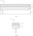
- FIG. 1 is a cross-sectional view of a structure of a capacitor 100' in a conventional technology.
- the capacitor 100' generally includes a substrate 110', a dielectric layer 140', and an electrode plate 150' that are sequentially arranged in a stacked structure.
- the dielectric layer 140' is located above the substrate 110'.
- the electrode plate 150' is located above the dielectric layer 140'.
- FIG. 2 is a schematic of an equivalent circuit of the capacitor 100' in FIG. 1 .
- an equivalent capacitor 200' in FIG. 2 is equivalent to equivalently connecting a resistor R' in series to a dielectric layer 240' and an electrode plate 250' in the capacitor 200'.
- the thickness d' of the substrate 110' may be reduced. This manner is intended to reduce the resistance value of the resistor R' introduced by the substrate 110' in the entire capacitor 100' by thinning the substrate 110', to reduce a high-frequency loss of the capacitor 100'.
- the substrate 110' due to a limitation of a preparation process, there is a bottleneck limitation on thinning of the substrate 110'. For example, it is difficult to reduce the thickness d' of the substrate 110' to less than 50 ⁇ m. Therefore, a degree of loss reduction is limited. More unsatisfactorily, because the substrate 110' has an unavoidable high-frequency loss, a non-negligible loss is still caused to the capacitor 100' regardless of the thickness d' of the substrate 110'. Because the substrate 110' is non-negligible, the resistor R' necessarily exists, and the resistance value of the resistor R' causes a high-frequency loss.
- embodiments of the present disclosure provide a capacitor capable of having an ultra-low loss at a high frequency and a method for preparing the capacitor.
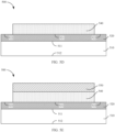
- FIG. 3 is a cross-sectional view of the capacitor 300.
- the capacitor 300 generally includes a substrate 310, a first electrode plate 320, a first dielectric layer 340, and a second electrode plate 350 that are of a stacked structure.
- the substrate 310 has a first surface 311 and a second surface 312 opposite to the first surface 311.
- the first electrode plate 320 is coupled to the first surface 311 of the substrate 310, and the first dielectric layer 340 and the second electrode plate 350 are sequentially disposed above the first electrode plate 320.
- FIG. 3 is a cross-sectional view of the capacitor 300.
- the capacitor 300 generally includes a substrate 310, a first electrode plate 320, a first dielectric layer 340, and a second electrode plate 350 that are of a stacked structure.
- the substrate 310 has a first surface 311 and a second surface 312 opposite to the first surface 311.
- the first electrode plate 320 is coupled to the first surface 311 of the substrate 310, and the first
- the substrate 310 is provided with a via 315 that runs through the first surface 311 to the second surface 312. A part of the first electrode plate 320 is exposed through the via 315.
- the capacitor 300 further has a plurality of conductive parts, including a first conductive part 331 disposed on the second surface 312 of the substrate 310, a second conductive part 332 disposed on a side that is of the first electrode plate 320 and that faces the via 315 (namely, the part that is of the first electrode plate 320 and that is exposed through the via 315), and a third conductive part 333 disposed on an inner wall 316 of the via 315.
- the first conductive part 331 may be coupled to the second conductive part 332 through the third conductive part 333, so that the conductive parts of the capacitor 300 are formed as a whole.
- the first electrode plate 320 is disposed on the first surface 311 of the substrate 310, a backside via process is applied to the second surface 312 of the substrate 310, and the conductive parts are applied to the second surface 312 of the substrate 310 and inside the via 315, so that the first surface 311 and the second surface 312 of the substrate 310 can be short-circuited through the conductive parts. In this way, effective bypass effect can be formed for the substrate 310.
- FIG. 4 is a schematic of an equivalent circuit of the capacitor 300 in FIG. 3 .
- the first electrode plate 320 and the substrate 310 are short-circuited through the first electrode plate 320, the via 315 that runs through the substrate 310, and the conductive parts of the capacitor 300 in FIG. 3 .
- resistors introduced by the first electrode plate 320 and the substrate 310 are negligible.
- a first dielectric layer 440 and a second electrode plate 450 in the equivalent capacitor 400 may be considered not to be connected in series to the equivalent resistor R'. In this way, a dielectric loss of the capacitor 300 in a high-frequency operating condition can be significantly reduced.
- the first conductive part 331, the second conductive part 332, and the third conductive part 333 may include at least one of the following materials: nickel, titanium, aluminum, lead, platinum, gold, titanium nitride, tantalum nitride, and copper.
- the conductive part may be made of any combination of these materials.
- the first electrode plate 320 disposed on the first surface 311 of the substrate 310 and the second surface 312 of the substrate 310 can be short-circuited through conduction effect of these conductive parts, to ensure reduction in the high-frequency loss.
- the materials listed herein are merely illustrative and are not exhaustive.
- the first conductive part 331, the second conductive part 332, and the third conductive part 333 may also be made of other conductive materials that are currently available or developed in the future, provided that such conductive materials can implement expected short-circuiting effect.
- a substrate 510 having a first surface 511 and a second surface 512 is provided.
- the substrate 510 may be made of a semiconductor wafer known in the industry or developed in the future.
- such a semiconductor wafer may be made of one or more of materials such as silicon, silicon carbide, gallium nitride, and aluminum nitride. It should be understood that the materials listed herein are merely illustrative and are not exhaustive.
- such a semiconductor wafer may be a conductive wafer, a semiinsulating wafer, or an insulating wafer. In other words, conductivity of the semiconductor wafer is not limited in this embodiment of the present disclosure.
- the figure shows that the first surface 511 and the second surface 512 of the substrate 510 are parallel, it should be noted that this is not necessary. There may be a specific non-zero included angle between the first surface 511 and the second surface 512.
- a first electrode plate 520 is provided above the first surface 511 of the substrate 510.
- the first electrode plate 520 is also referred to as a lower electrode plate.
- the first electrode plate 520 may be made of metal, for example, one or more of gold, silver, aluminum, nickel, titanium, platinum, copper, tungsten, tin, and tantalum.
- the first electrode plate 520 may alternatively be made of an alloy material, for example, one or more of titanium nitride, tungsten silicide, and tantalum nitride. It should be understood that the materials listed herein are merely illustrative, but are not limitative.
- first electrode plate 520 A person skilled in the art may consider another material to prepare the first electrode plate 520.
- a layer of metal may be deposited through electron beam evaporation, magnetron sputtering, or the like, to form the first electrode plate 520. It should be noted that the deposition manner described herein is merely for description but not a limitation. The material may be deposited in another deposition manner that is known or developed in the future, to provide the first electrode plate 520 above the first surface 511 of the substrate 510.
- a first dielectric layer 540 is deposited above the first electrode plate 520.
- a thickness of the first dielectric layer 540 may range from 20 nm to 500 nm. It should be noted that the values herein are merely illustrative, but are not limitative.
- the first dielectric layer 540 may include at least one of the following materials: silicon nitride, silicon oxide, silicon oxynitride, silicon oxide, aluminum oxide, and titanium oxide.
- the first dielectric layer 540 may be of a single-layer structure, or may be of a multi-layer stacked structure. A specific structure of the first dielectric layer 540 is not limited in this embodiment of the present disclosure.
- a first part 521 and a second part 522 different from the first part 521 may be determined on the first electrode plate 520.
- a part that is of the first dielectric layer 540 and that is coupled to the second part 522 may be removed through an etching process, and a part that is of the first dielectric layer 540 and that is coupled to the first part 521 may be retained, to form the final first dielectric layer 540.
- an unnecessary part may be etched out through an appropriate process, and a part of a dielectric material may be retained, to form the first dielectric layer 540.
- an area that is of the first dielectric layer 540 and that needs to be retained may be calculated based on required capacitance of the final capacitor 500 that needs to be obtained.
- a specific calculation method is not limited in this embodiment of the present disclosure.
- the final first dielectric layer 540 may be obtained through various wet etching or dry etching processes.
- a second electrode plate 550 is provided above the first dielectric layer 540.
- the second electrode plate 550 is also referred to as an upper electrode plate.
- the second electrode plate 550 may be made of a metal material, for example, one or more of gold, silver, aluminum, nickel, titanium, platinum, copper, tungsten, tin, and tantalum.
- the second electrode plate 550 may be made of an alloy material, for example, one or more of titanium nitride, tungsten silicide, and tantalum nitride.
- the second electrode plate 550 may be made of a material the same as that of the first electrode plate 520, or may be made of a material different from that of the first electrode plate 520.
- a metal graphic of the second electrode plate 550 may be determined by using a lithography process. In some other embodiments, the graphic may alternatively be obtained through a metal evaporation process or a metal dry etching process. It should be understood that the process mentioned herein is merely illustrative.
- a second dielectric layer 560 may be formed above the second electrode plate 550.
- a thickness of the second dielectric layer 560 may range from 20 nm to 2000 nm. It should be noted that the values herein are merely illustrative, but are not limitative.
- the second dielectric layer 560 may include at least one of the following materials: silicon nitride, silicon oxide, silicon oxynitride, silicon oxide, aluminum oxide, and titanium oxide. It should be understood that the materials listed herein are merely illustrative, but are not limitative. A person skilled in the art may consider another material to prepare the second dielectric layer 560.
- the second dielectric layer 560 may be made of a material the same as that of the first dielectric layer 540. In some other embodiments, the second dielectric layer 560 may alternatively be made of a material different from that of the first dielectric layer 540.
- the second dielectric layer 560 may be of a single-layer structure, or may be of a multi-layer stacked structure. A specific structure of the second dielectric layer 560 is not limited in this embodiment of the present disclosure.
- a part of the second dielectric layer 560 may be removed from the second electrode plate 550 through an etching process, and a remaining part of the second dielectric layer 560 may be retained, to form the final second dielectric layer 560.
- an unnecessary part may be etched out through an appropriate process, and a part of a dielectric material may be retained, to form the second dielectric layer 560.
- the second dielectric layer 560 may be referred to as a wrapping layer, and is configured to protect other components of the capacitor 500 from being affected by moisture, impact, or the like.
- the final second dielectric layer 560 may be obtained through various wet etching or dry etching processes.
- the second dielectric layer 560 may be obtained through a process the same as that of the first dielectric layer 540, or may be obtained through a process different from that of the first dielectric layer 540.
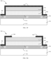
- FIG. 5H As shown in the figure, deep via etching is performed on the second surface 512 of the substrate 510, to obtain a via 515 shown in the figure.
- the via 515 is etched, so that a part of the first electrode plate 520 is exposed, and an inner wall 516 of the via 515 is also exposed.
- two vias 515 are shown in the figure, this is not limitative. A quantity of vias 515 may be determined based on an actual process requirement.
- the two vias 515 shown in FIG. 5H extend parallel to each other. In this way, the part of the via 515 and the part of the first electrode plate 520 can be exposed.
- a metal laminated material is deposited on a side of the second surface 512 of the substrate 510.
- Such a metal laminated material is deposited on the first surface 512 of the substrate 510, the exposed part of the first electrode plate 520, and the inner wall 516 of the via 515, to correspondingly form a first conductive part 531, a second conductive part 532, and a third conductive part 533.
- the first conductive part 531 is coupled to the second conductive part 532 through the third conductive part 533, so that the conductive parts are formed as a whole.
- thicknesses of the first conductive part 531, the second conductive part 532, and the third conductive part 533 may range from 20 nm to 1500 nm. It should be noted that the values herein are merely illustrative, but are not limitative.
- the first conductive part 531, the second conductive part 532, and the third conductive part 533 may include at least one of the following materials: nickel, titanium, aluminum, lead, platinum, gold, titanium nitride, tantalum nitride, and copper. It should be understood that the materials listed herein are merely illustrative, but are not limitative. A person skilled in the art may consider another material to prepare these conductive parts.
- the second surface 512 of the substrate 510 and the first electrode plate 520 may be short-circuited through the conductive parts that are coupled to each other and that are approximately in a square wave shape. In this way, effective bypass effect can be formed for the substrate 510 and the first electrode plate 520, to ensure reduction in a high-frequency loss.
- FIG. 5A to FIG. 5I show examples of steps of preparing the capacitor 500, it should be understood that these steps do not need to be performed strictly based on the order shown in the figures, and some steps may be exchanged with each other.
- a graphic of the first dielectric layer 540 is first formed, and then, the second electrode plate 550 is provided above the first dielectric layer 540 whose graphic has been determined.
- the first dielectric layer 540 and the second electrode plate 550 may alternatively be graphically defined after the first dielectric layer 540 and the second electrode plate 550 are formed above the entire surface of the first electrode plate 520.
- the via 515 is formed after the first dielectric layer 540, the second electrode plate 550, and the second dielectric layer 560 are formed.
- the via 515 may alternatively be formed before the first dielectric layer 540, the second electrode plate 550, and the second dielectric layer 560 are formed, or may be formed in synchronization with the first dielectric layer 540, the second electrode plate 550, and the second dielectric layer 560.
- Such a step should also be considered to fall into embodiments of the present disclosure.
- the components in the figure are not drawn in proportion, and a size relationship between these components is merely illustrative.
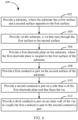
- FIG. 6 shows, in a form of a block diagram, a preparation method 600 according to a second aspect of the present disclosure, to prepare the semiconductor device 500 mentioned above.
- a substrate 510 having a first surface 511 and a second surface 512 is provided.
- the substrate 510 may be, for example, a wafer commonly mentioned in the art.
- the substrate 510 is provided with a via 515 that runs through the first surface 511 to the second surface 512. This can be implemented in any appropriate manner.
- a first electrode plate 520 is provided on the first surface 511 of the substrate 510, so that the first electrode plate 520 is coupled to the first surface 511.
- a first conductive part 531 is provided on the second surface 512 of the substrate 510.
- a second conductive part 532 is formed on a surface that is exposed through the via 515 and that is of a side that is of the first electrode plate 520 and that faces the via 515, and a third conductive part 533 is formed on an inner wall 516 of the via 515.
- the second conductive part 532 is coupled to the first conductive part 531 through the third conductive part 533.
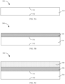
- FIG. 7A and FIG. 7B are top views of a capacitor 700 according to an example of an embodiment of the present disclosure. Some examples of structures and layouts of vias 715 and a position relationship between the vias 715 and a second electrode plate 750 can be seen.
- a cross section of the via 715 may be approximately elliptical.
- the via 715 may alternatively be in a long strip shape.
Landscapes
- Engineering & Computer Science (AREA)
- Power Engineering (AREA)
- Microelectronics & Electronic Packaging (AREA)
- Manufacturing & Machinery (AREA)
- Semiconductor Integrated Circuits (AREA)
- Fixed Capacitors And Capacitor Manufacturing Machines (AREA)
Applications Claiming Priority (1)
| Application Number | Priority Date | Filing Date | Title |
|---|---|---|---|
| PCT/CN2022/088747 WO2023205939A1 (zh) | 2022-04-24 | 2022-04-24 | 电容器及其制备方法 |
Publications (2)
| Publication Number | Publication Date |
|---|---|
| EP4468367A1 true EP4468367A1 (de) | 2024-11-27 |
| EP4468367A4 EP4468367A4 (de) | 2025-10-22 |
Family
ID=88516659
Family Applications (1)
| Application Number | Title | Priority Date | Filing Date |
|---|---|---|---|
| EP22938798.0A Pending EP4468367A4 (de) | 2022-04-24 | 2022-04-24 | Kondensator und herstellungsverfahren dafür |
Country Status (4)
| Country | Link |
|---|---|
| EP (1) | EP4468367A4 (de) |
| JP (1) | JP2025511636A (de) |
| CN (1) | CN118541810A (de) |
| WO (1) | WO2023205939A1 (de) |
Families Citing this family (1)
| Publication number | Priority date | Publication date | Assignee | Title |
|---|---|---|---|---|
| CN119677403B (zh) * | 2024-12-10 | 2026-03-13 | 广州增芯科技有限公司 | Mim电容器件及其制备方法 |
Family Cites Families (11)
| Publication number | Priority date | Publication date | Assignee | Title |
|---|---|---|---|---|
| JP3246166B2 (ja) * | 1994-03-03 | 2002-01-15 | 株式会社村田製作所 | 薄膜コンデンサ |
| JP4402271B2 (ja) * | 2000-08-18 | 2010-01-20 | 三菱電機株式会社 | キャパシタとこのキャパシタを有する半導体装置 |
| JP4548262B2 (ja) * | 2005-07-29 | 2010-09-22 | Tdk株式会社 | 下部電極構造 |
| US8003479B2 (en) * | 2006-03-27 | 2011-08-23 | Intel Corporation | Low temperature deposition and ultra fast annealing of integrated circuit thin film capacitor |
| CN102074588A (zh) * | 2009-11-20 | 2011-05-25 | 中芯国际集成电路制造(上海)有限公司 | Mim电容器及其制造方法、集成电路的制造方法 |
| US8649153B2 (en) * | 2011-04-28 | 2014-02-11 | International Business Machines Corporation | Tapered via and MIM capacitor |
| US10622284B2 (en) * | 2016-06-24 | 2020-04-14 | Infineon Technologies Ag | LDMOS transistor and method |
| US10242932B2 (en) * | 2016-06-24 | 2019-03-26 | Infineon Technologies Ag | LDMOS transistor and method |
| CN111199956A (zh) * | 2018-11-19 | 2020-05-26 | 中芯国际集成电路制造(天津)有限公司 | 一种半导体器件及其形成方法 |
| US11558018B2 (en) * | 2020-01-29 | 2023-01-17 | Nxp Usa, Inc. | Integrated circuits containing vertically-integrated capacitor-avalanche diode structures |
| CN115088071A (zh) * | 2020-02-17 | 2022-09-20 | 株式会社村田制作所 | 半导体装置以及模块 |
-
2022
- 2022-04-24 JP JP2024557681A patent/JP2025511636A/ja active Pending
- 2022-04-24 CN CN202280088965.3A patent/CN118541810A/zh active Pending
- 2022-04-24 EP EP22938798.0A patent/EP4468367A4/de active Pending
- 2022-04-24 WO PCT/CN2022/088747 patent/WO2023205939A1/zh not_active Ceased
Also Published As
| Publication number | Publication date |
|---|---|
| CN118541810A (zh) | 2024-08-23 |
| EP4468367A4 (de) | 2025-10-22 |
| WO2023205939A1 (zh) | 2023-11-02 |
| JP2025511636A (ja) | 2025-04-16 |
Similar Documents
| Publication | Publication Date | Title |
|---|---|---|
| US11101072B2 (en) | Capacitor with limited substrate capacitance | |
| US9093419B2 (en) | Semiconductor device containing MIM capacitor and fabrication method | |
| US10998279B2 (en) | On-chip integrated cavity resonator | |
| JP2002536904A (ja) | ワイドバンドインピーダンスカプラー | |
| JP2005500773A (ja) | 表面実装用途向けミリ波フィルタ | |
| EP4468367A1 (de) | Kondensator und herstellungsverfahren dafür | |
| WO2001031706A1 (en) | Methods for forming co-axial interconnect lines in a cmos process | |
| AU2021311004B2 (en) | Superconducting structure and device surface termination with alloy | |
| US9502382B2 (en) | Coplaner waveguide transition | |
| CN103219376B (zh) | 氮化镓射频功率器件及其制备方法 | |
| CN113497598B (zh) | 体声波谐振器和体声波滤波器装置 | |
| US5834995A (en) | Cylindrical edge microstrip transmission line | |
| CN103219379B (zh) | 一种采用先栅工艺的高电子迁移率器件及其制备方法 | |
| JP3518249B2 (ja) | 高周波回路素子 | |
| JP4151455B2 (ja) | モノリシックマイクロ波集積回路およびその製造方法 | |
| CN117015299A (zh) | 电容器结构及其形成方法 | |
| CN220963708U (zh) | 一种硅基GaN宽阻带高选择性毫米波在片滤波器 | |
| JP4464104B2 (ja) | マイクロ波集積回路 | |
| KR960016229B1 (ko) | 반도체소자의 콘택구조 및 그 제조방법 | |
| US20220254717A1 (en) | Semiconductor Device And Manufacturing Method Therefor | |
| CN222321833U (zh) | 细线路结构 | |
| CN100524732C (zh) | 电磁噪声抑制体及电磁噪声抑制方法 | |
| JPH11163272A (ja) | マイクロ波回路 | |
| CN117525782A (zh) | 硅基氮化镓宽阻带高选择性片上带通滤波器及其制备方法 | |
| CN116634851A (zh) | 超导电路及其保护方法 |
Legal Events
| Date | Code | Title | Description |
|---|---|---|---|
| STAA | Information on the status of an ep patent application or granted ep patent |
Free format text: STATUS: THE INTERNATIONAL PUBLICATION HAS BEEN MADE |
|
| PUAI | Public reference made under article 153(3) epc to a published international application that has entered the european phase |
Free format text: ORIGINAL CODE: 0009012 |
|
| STAA | Information on the status of an ep patent application or granted ep patent |
Free format text: STATUS: REQUEST FOR EXAMINATION WAS MADE |
|
| 17P | Request for examination filed |
Effective date: 20240822 |
|
| AK | Designated contracting states |
Kind code of ref document: A1 Designated state(s): AL AT BE BG CH CY CZ DE DK EE ES FI FR GB GR HR HU IE IS IT LI LT LU LV MC MK MT NL NO PL PT RO RS SE SI SK SM TR |
|
| DAV | Request for validation of the european patent (deleted) | ||
| DAX | Request for extension of the european patent (deleted) | ||
| REG | Reference to a national code |
Ref country code: DE Ref legal event code: R079 Free format text: PREVIOUS MAIN CLASS: H01L0029780000 Ipc: H01G0004330000 |
|
| A4 | Supplementary search report drawn up and despatched |
Effective date: 20250918 |
|
| RIC1 | Information provided on ipc code assigned before grant |
Ipc: H01G 4/33 20060101AFI20250912BHEP Ipc: H01G 4/005 20060101ALI20250912BHEP Ipc: H01G 4/228 20060101ALI20250912BHEP Ipc: H01L 21/768 20060101ALI20250912BHEP Ipc: H01L 21/02 20060101ALI20250912BHEP Ipc: H01L 23/522 20060101ALI20250912BHEP Ipc: H10D 1/62 20250101ALI20250912BHEP Ipc: H01G 4/012 20060101ALI20250912BHEP Ipc: H01L 23/48 20060101ALI20250912BHEP |