EP4468647A1 - Synchronisationssteuerungsverfahren, endgerätevorrichtung, netzwerkvorrichtung, chip und speichermedium - Google Patents
Synchronisationssteuerungsverfahren, endgerätevorrichtung, netzwerkvorrichtung, chip und speichermedium Download PDFInfo
- Publication number
- EP4468647A1 EP4468647A1 EP22921159.4A EP22921159A EP4468647A1 EP 4468647 A1 EP4468647 A1 EP 4468647A1 EP 22921159 A EP22921159 A EP 22921159A EP 4468647 A1 EP4468647 A1 EP 4468647A1
- Authority
- EP
- European Patent Office
- Prior art keywords
- signal
- terminal device
- uplink
- sequence
- information
- Prior art date
- Legal status (The legal status is an assumption and is not a legal conclusion. Google has not performed a legal analysis and makes no representation as to the accuracy of the status listed.)
- Pending
Links
Images




Classifications
-
- H—ELECTRICITY
- H04—ELECTRIC COMMUNICATION TECHNIQUE
- H04W—WIRELESS COMMUNICATION NETWORKS
- H04W56/00—Synchronisation arrangements
- H04W56/0035—Synchronisation arrangements detecting errors in frequency or phase
-
- H—ELECTRICITY
- H04—ELECTRIC COMMUNICATION TECHNIQUE
- H04W—WIRELESS COMMUNICATION NETWORKS
- H04W56/00—Synchronisation arrangements
-
- H—ELECTRICITY
- H04—ELECTRIC COMMUNICATION TECHNIQUE
- H04W—WIRELESS COMMUNICATION NETWORKS
- H04W56/00—Synchronisation arrangements
- H04W56/001—Synchronization between nodes
Definitions
- the present application relates to the field of communications, and in particular, to synchronization control methods, terminal devices, network devices, a chip, a computer-readable storage medium, a computer program product, a computer program and a communication system.
- Timing accuracy of communication devices directly affects communication performance.
- some terminal devices such as zero-power terminals
- embodiments of the present application provide synchronization control methods, terminal devices, network devices, a chip, a computer-readable storage medium, a computer program product, a computer program and a communication system, which may be used to solve a problem regarding timing adjustments.
- Embodiments of the present application further provide a terminal device, and the terminal device includes a processor and a memory.
- the memory is configured to store a computer program
- the processor is configured to call and run the computer program stored in the memory to perform the synchronization control method provided by any embodiment of the present application.
- Embodiments of the present application further provide a network device, and the network device includes a processor and a memory.
- the memory is configured to store a computer program
- the processor is configured to call and run the computer program stored in the memory to perform the synchronization control method provided by any embodiment of the present application.
- Embodiments of the present application further provide a chip, and the chip includes a processor configured to call and run a computer program from a memory to cause a device equipped with the chip to perform the synchronization control method provided by any embodiment of the present application.
- Embodiments of the present application further provide a computer-readable storage medium, and the computer-readable storage medium configured to store a computer program.
- the computer program causes a computer to perform the synchronization control method provided by any embodiment of the present application.
- Embodiments of the present application further provide a computer program product, and the computer program product includes computer program instructions.
- the computer program instructions cause a computer to perform the synchronization control method provided by any embodiment of the present application.
- Embodiments of the present application further provide a computer program, and the computer program causes a computer to perform the synchronization control method provided by any embodiment of the present application.
- Embodiments of the present application further provide a communication system, and the communication system includes a terminal device and a network device, which are configured to perform the synchronization control method provided by any embodiment of the present application.
- the terminal device performs uplink communication based on back scattering, where the terminal device modulates a reflected signal of a downlink signal sent by the network device to obtain an uplink signal carrying synchronization information, and the network device may obtain a timing error and/or frequency error of the terminal device based on the synchronization information. Therefore, the network device may correct or assist the terminal device in correcting the timing error and/or frequency error to improve timing accuracy, thereby ensuring that the terminal device and the network device transceive information with accurate timing.
- GSM global system of mobile communication
- CDMA code division multiple access
- WCDMA wideband code division multiple access
- GPRS general packet radio service
- LTE long term evolution
- LTE-A advanced long term evolution
- NR new radio
- evolution system of the NR system an LTE-based access to unlicensed spectrum (LTE-U) system, an NR-based access to unlicensed spectrum (NR-U) system, a non-terrestrial networks (NTN) system, a universal mobile telecommunication system (UMTS), wireless local area networks (WLAN), wireless fidelity (Wi-Fi), a 5th-generation (5G) system, or other communication systems.
- GSM global system of mobile communication
- CDMA code division multiple access
- WCDMA wideband code division multiple access
- GPRS general packet radio service
- LTE long term evolution
- LTE-A advanced long term evolution
- NR new radio
- NTN non-terrestrial networks
- UMTS universal mobile telecommunication system
- WLAN wireless local area networks
- D2D device to device
- M2M machine to machine
- MTC machine type communication
- V2V vehicle to vehicle
- V2X vehicle to everything
- a communication system in the embodiments of the present application may be applied to a carrier aggregation (CA) scenario, a dual connectivity (DC) scenario, or a standalone (SA) networking scenario.
- CA carrier aggregation
- DC dual connectivity
- SA standalone
- the embodiments of the present application describe various embodiments in conjunction with a network device and a terminal device.
- the terminal device may also be referred to as a user equipment (UE), an access terminal, a user unit, a user station, a mobile station, a mobile platform, a remote station, a remote terminal, a mobile device, a user terminal, a terminal, a wireless communication device, a user agent, a user device, or the like.
- UE user equipment
- the terminal device may be a station (ST) in WLAN, which may be a cellular phone, a cordless phone, a session initiation protocol (SIP) phone, a wireless local loop (WLL) station, a personal digital assistant (PDA) device, a handheld device with wireless communication functions, a computing device or other processing devices connected to a wireless modem, an in-vehicle device, a wearable device, a terminal device in a next-generation communication system (such as an NR network), a terminal device in a future evolved public land mobile network (PLMN) network, or the like.
- ST station
- WLAN which may be a cellular phone, a cordless phone, a session initiation protocol (SIP) phone, a wireless local loop (WLL) station, a personal digital assistant (PDA) device, a handheld device with wireless communication functions, a computing device or other processing devices connected to a wireless modem, an in-vehicle device, a wearable device, a terminal device in a next-generation communication
- the terminal device may be deployed on land, including indoor or outdoor, handheld, wearable, or in-vehicle; the terminal device may also be deployed on water (e.g., on a steamship); and the terminal device may also be deployed in air (e.g., on an airplane, on a balloon, or on a satellite).
- the terminal device may be a mobile phone, a pad, a computer with a wireless transceiver function, a virtual reality (VR) terminal device, an augmented reality (AR) terminal device, a wireless terminal device in industrial control, a wireless terminal device in self driving, a wireless terminal device in remote medical, a wireless terminal device in smart grid, a wireless terminal device in transportation safety, a wireless terminal device in smart city, a wireless terminal device in smart home, or the like.
- VR virtual reality
- AR augmented reality
- the terminal device may also be a wearable device.
- the wearable device may also be referred to as a wearable smart device, which is a general term for wearable devices developed by using wearable technology and intelligent design for everyday wear, such as glasses, gloves, a watch, clothing, or shoes.
- the wearable device is a portable device that is worn directly on a body, or integrated into a user's clothing or accessories.
- the wearable device is not only a hardware device, but also implements powerful functions through software support as well as data interaction or cloud interaction.
- Generalized wearable smart devices include full-featured, large-sized devices that may implement full or partial functionality without relying on smart phones, such as a smart watch or smart glasses, and devices that focus on a certain type of application functionality only and need to be used in conjunction with other devices (such as smart phones), such as various smart bracelets or smart jewelries for monitoring physical signs.
- the network device may be a device for communicating with a mobile device, such as an access network device.
- the network device may be an access point (AP) in WLAN, a base station (Base Transceiver Station, BTS) in GSM or CDMA, a base station (NodeB, NB) in WCDMA, an evolved base station (Evolutional NodeB, eNB or eNodeB) in LTE, a relay station or access point, an in-vehicle device, a wearable device, a network device (gNB) in an NR network, or a network device in a future evolved PLMN network, or the like.
- AP access point
- BTS Base Transceiver Station
- NodeB, NB base station
- Evolutional NodeB, eNB or eNodeB evolved base station
- gNB network device
- gNB network device in an NR network
- future evolved PLMN network or the like.
- the network device may also be a core network device, such as a mobility management entity (MME), an access and mobility management function (AMF) entity, or other network entities, which is not limited in the embodiments of the present application.
- MME mobility management entity
- AMF access and mobility management function
- the network device may have a mobile characteristic.
- the network device may be mobile equipment.
- the network device may be a satellite or a balloon station.
- the satellite may be a low earth orbit (LEO) satellite, a medium earth orbit (MEO) satellite, a geostationary earth orbit (GEO) satellite, a high elliptical orbit (HEO) satellite, or the like.
- the network device may also be a base station set up on land, water, or the like.
- the network device may provide services for a cell, and the terminal device may communicate with the network device through transmission resources (e.g., frequency domain resources, or spectrum resources) used by the cell.
- the cell may be a cell corresponding to the network device (e.g., a base station).
- the cell may belong to a macro base station or a base station corresponding to a small cell.
- the small cell here may include: a metro cell, a micro cell, a pico cell, a femto cell, etc. These small cells have characteristics of small coverage and low transmission power, and are suitable for providing high-speed data transmission services.
- FIG. 1 schematically shows a wireless access system 1000 including a network device 1100 and two terminal devices 1200.
- the wireless communication system 1000 may include multiple network devices 1100, and coverage area of each network device 110 may be provided therein with other number of terminal devices.
- a device in a network/system having a communication function in the embodiments of the present application may be referred to as a communication device.
- the communication devices may include the network device and the terminal devices, which have the communication function.
- the network device and the terminal devices may be specific devices in the embodiments of the present application.
- system and “network” are often used interchangeably herein.
- the term “and/or” herein is used to describe an association relationship between associated objects, for example, to indicate that there may be three relationships between the related objects.
- a and/or B may represent: A alone, both A and B, and B alone.
- the character “/” herein generally indicates that related objects before and after this character are in an "or” relationship.
- indicate may mean a direct indication or an indirect indication, or represent that there is an association relationship.
- a indicating B may mean that A directly indicates B, e.g., that B may be obtained through A; or it may mean that A indirectly indicates B, e.g., that A indicates C, and B may be obtained through C; or it may mean that there is an association relationship between A and B.
- correlate described in the embodiments of the present application may mean a relationship of direct or indirect correspondence between the two, or a relationship of association between the two, or a relationship of indicating and being indicated, or configuring and being configured, or the like.
- a typical zero-power device is a radio frequency identification (RFID) device, which uses radio coupling between a receiving terminal and a transmitting terminal to achieve contactless automatic transmission and identification of tag information. This includes inductive coupling at short distances and electromagnetic coupling at long distances.
- RFID tag is also called "radio frequency tag” or "electronic tag”.
- electronic tags may be categorized into three types of tags, i.e., active electronic tags, passive electronic tags and semi-passive electronic tags.
- An active electronic tag also called an electronic tag with active mode, refers to an electronic tag with built-in battery to provide power for working. Unlike passive radio frequency activation, this tag may actively send information in a set frequency band.
- the passive electronic tags also called an electronic tag with passive mode, does not support built-in battery.
- an antenna of the electronic tag When a passive electronic tag approaches a reader-writer, an antenna of the electronic tag is in a near field formed by radiation of an antenna of the reader-writer and generates an induced current through electromagnetic induction, and the induced current drives a chip circuit in the electronic tag.
- the chip circuit sends identification information stored in the tag to the reader-writer through the antenna of the electronic tag.
- the semi-active electronic tag inherits advantages of the passive electronic tag, such as small size, light weight, low price and long service life.
- a built-in battery of the semi-active electronic tag only supplies power for a small number of circuits in a chip. Only when the reader-writer accesses, the built-in battery supplies power to an RFID chip to increase reading and writing distances of the tag and improve reliability of communication.
- the most basic RFID system using wireless communication technology consists of two parts: an electronic tag (TAG) and a reader-writer (Reader/Writer).
- the electronic tag is composed of a coupling component and a chip.
- Each electronic tag has a unique electronic number and is placed on a target to be measured to achieve a purpose of marking the target object.
- the reader-writer may not only read information on the electronic tag, but also write information into the electronic tag, and provide power required for communication for the electronic tag.
- the reader-writer reads the information and decodes it to identify the electronic tag.
- RFID is a typical zero-power communication.
- Key technologies of such zero-power communication include power harvesting, back scattering communication and low-power computing.
- a typical zero-power communication system includes a reader-writer and a zero-power terminal.
- the reader-writer transmits radio waves for providing power to the zero-power terminal.
- a power harvesting module installed in the zero-power terminal may harvest power carried by radio waves in space (radio waves transmitted by the reader-writer as shown in FIG. 2 ), to drive a low-power computing module of the zero-power terminal and realize back scattering communication.
- the zero-power terminal After the zero-power terminal obtains the power, it may receive a control command from the reader-writer and send data to the reader-writer based on the control signaling and back scattering.
- the sent data may come from data stored in the zero-power terminal itself (such as an identification identifier or pre-written information, for example, a production date, a brand, a manufacturer of a product).
- the zero-power terminal may also be provided with various sensors, so as to report data collected by the various sensors based on a zero-power mechanism.
- Zero-power communication Communication based on a zero-power device, referred to as zero-power communication, includes following key technologies.
- a zero-power device such as a back scattering tag shown in FIG. 3 , receives a carrier signal sent by a back scattering reader-writer, and harvests power through an RF power harvesting module, which is supplied to a low-power processing module (a logic processing module shown in FIG. 3 ) to modulate an incoming signal and perform back scattering.
- a low-power processing module a logic processing module shown in FIG. 3
- an RF module is utilized to harvest power of electromagnetic waves in space through electromagnetic induction, which may achieve drive of a load circuit (low-power computing, sensor, etc.), thereby achieving battery-free.
- Load modulation is a method often used by an electronic tag to transmit data to a reader-writer.
- the load modulation completes a modulation process by adjusting electrical parameters of an oscillation circuit of the electronic tag according to rhythms of a data stream to change a size and phase of impedance of the electronic tag accordingly.
- resistive load modulation a resistor is connected in parallel with a load, which is called a load modulation resistor.
- the resistor is turned on and off according to a clock of the data stream, and the on-off of a switch S is controlled by binary data encoding.
- the circuit schematic diagram of the resistive load modulation is shown in FIG. 5 .
- a capacitor is connected in parallel with a load, replacing the load modulation resistor controlled by the binary data encoding shown in FIG. 5 .
- Data transmitted by an electronic tag may be represented by binary "1" and "0” by using codes with different forms.
- a wireless radio frequency identification system usually use one of following encoding methods: non-return-to-zero (NRZ) encoding, Manchester encoding, unipolar return-to-zero (Unipolar RZ) encoding, differential bi-phase (DBP) encoding, Miller encoding, and differential encoding. In layman's terms, different pulse signals are used to represent 0 and 1.
- the passive Internet of Things device may be used in the cellular Internet of Things based on existing zero-power devices.
- Subcarrier modulation means that carrier 1 is first modulated with a signal, and then another carrier 2 with a higher frequency is modulated based on the modulation result.
- the subcarrier modulation is a modulation scheme often used in an RFID system.
- the zero-power terminal in the above-mentioned related technologies needs to be provided with a power supply signal through a network device (such as a base station, or an RFID reader-writer) or other sources, so that the zero-power terminal may obtain power to drive a circuit.
- a clock is also provided in the circuit of the zero-power terminal.
- a zero-power clock circuit portion often uses a simplified circuit of an RC oscillator. Timing, frequency, phase and other errors of such circuit are relatively large.
- FIGS. 6A and 6B are schematic diagrams showing a timing signal error of a zero-power consumption terminal based on actual tests. Specific data are as follows.
- a zero-power device using a microcontroller may further correct the error, it is still much higher than an error of a crystal oscillator circuit.
- the present application proposes to further control an error of a reflected signal by a network. Otherwise, a timing error and its accumulated value may cause a system to fail to communicate normally. In addition, since frequency of a signal reflected by the terminal is different from frequency of continuous waves for power supply, there is a lack of reference signal calibration.
- Solutions provided in the embodiments of the present application is mainly used to solve at least one of above problems.
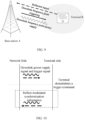
- FIG. 7 is a schematic flowchart of a synchronization control method, in accordance with an embodiment of the present application.
- the method may optionally be applied to the system shown in FIG. 1 , but it is not limited thereto.
- the method includes:
- FIG. 8 is a schematic flowchart showing a synchronization control method, in accordance with another embodiment of the present application. The method may also optionally be applied to the system shown in FIG. 1 , but it is not limited thereto. The method includes:
- the terminal device performs uplink communication based on back scattering, where modulation is performed on a reflected signal of a downlink signal sent by the network device to obtain an uplink signal carrying synchronization information; and the network device may obtain a timing error and/or frequency error of the terminal device based on the synchronization information. Therefore, the network device may correct or assist the terminal device in correcting the timing error and/or frequency error, to improve timing accuracy and ensure that the terminal device and the network device transceive information with accurate timing.
- uplink reflection is integrated with an uplink synchronization reference signal, spectrum resources may be saved.
- the terminal device may include a terminal based on back scattering communication, such as a zero-power terminal, a semi-active terminal, or the like.
- the network device may include a power supply node and a receiving base station for zero-power communication, and may also include a network device in other communication systems for assisting the terminal in timing correction.
- the embodiments of the present application support a solution in which the power supply node and the receiving base station are separated or integrated.
- the network device may include a single device, which acts both as a power supply node to provide power to the terminal device and as a receiving base station to receive an uplink signal sent by the terminal device.
- the network device may also include multiple devices, including a functional node and a receiving base station that are independent of each other.
- coordination link interface(s) are provided between the functional node and the receiving base station.
- the first downlink signal sent by the network device may be used for power supply and information transmission.
- the first downlink signal may include a power supply signal and a signal for information transmission.
- the signal for information transmission may be specifically used for transmitting downlink information to the terminal device based on service requirements to trigger the terminal device to transmit uplink information by using a back scattering technology, and therefore, this signal may also be called a trigger signal.
- the first downlink signal may also include a signal used for both power supply and information transmission.
- the functional signal and the signal for information transmission sent by the network device may be two signals or a same signal.
- the two signals may be sent at different frequency points or at a same frequency point.
- the power supply signal may be continuously or intermittently sent by the network device (e.g., a base station or a power supply node) in a downlink frequency band.
- the power supply signal may be a continuous wave (CW), such as a sine wave.
- the terminal device receives the first downlink signal, performs power harvesting, and demodulates a trigger signal. After the terminal device obtains power, it may perform corresponding functions, such as signal reception, signal transmission, measurement, or the like. In the embodiments of the present application, the terminal device modulates synchronization information into a reflected signal of the first downlink signal, so that the network device may estimate the timing error and/or frequency error of the terminal device.
- the synchronization information may include a synchronization signal sequence carried in the first uplink signal, which may also be understood as timing, frequency and other information of the terminal device obtained based on the synchronization signal sequence.
- performing, by the terminal device, modulation on the reflected signal of the first downlink signal includes: performing, by the terminal device, modulation on the reflected signal based on a synchronization signal sequence. That is, the first uplink signal is obtained by performing modulation on the reflected signal based on the synchronization signal sequence.
- a terminal may use a modulation scheme, such as amplitude modulation (ASK), frequency modulation (FSK), phase modulation (PSK), or the like. That is, the first uplink signal is obtained by modulating the synchronization signal sequence onto the reflected signal based on an amplitude modulation scheme, a frequency modulation scheme or a phase modulation scheme.
- performing, by the terminal device, modulation on the reflected signal based on the synchronization signal sequence includes: modulating, by the terminal device, the synchronization signal sequence onto the reflected signal based on the amplitude modulation scheme, the frequency modulation scheme or the phase modulation scheme.
- the synchronization signal sequence may be a sequence with a high time domain autocorrelation characteristic.
- the synchronization signal sequence may include a pseudo noise (PN) sequence, a discrete Fourier transform (DFT) sequence, or a constant amplitude zero autocorrelation (CAZAC) sequence.
- PN sequence may also be called a pseudo-random (Pseudo-Random) sequence.
- the PN sequence may include an M sequence or a Gold sequence, etc.
- other information may also be modulated in the first uplink signal, such as uplink information related to a service or transmission control. That is, performing modulation on the reflected signal to obtain the first uplink signal is further based on uplink information. Specifically, performing, by the terminal device, modulation on the reflected signal of the first downlink signal, further includes: performing, by the terminal device, modulation on the reflected signal based on uplink information.
- the first uplink signal is obtained by modulating, based on a subcarrier modulation scheme, uplink information onto a reflected signal that has been modulated based on a synchronization signal sequence. That is, the synchronization signal sequence may be modulated onto the reflected signal first, and then the uplink information may be directly modulated onto the synchronization signal sequence.
- performing, by the terminal device, modulation on the reflected signal based on the uplink information includes: modulating, by the terminal device based on the subcarrier modulation scheme, the uplink information onto the reflected signal that has been modulated based on the synchronization signal sequence.
- the uplink information and the synchronization information may also be modulated onto the reflected signal in a time division multiplexing manner. That is, the uplink information is multiplexed with the synchronization signal sequence in a time division manner.
- the uplink information includes at least one of the following information:
- the first downlink signal and the first uplink signal use a same frequency point.
- the optional method it is allowed to use the same uplink and downlink frequency point to solve an uplink and downlink interference problem by means of different transmitting node and receiving node, so that uplink and downlink spectrum resources may be well utilized.
- the network device may perform timing correction on an uplink signal based on the synchronization information.
- a timing error and/or frequency error of the terminal device obtained based on the synchronization information may be used by the network device to perform timing adjustment and/or frequency adjustment on the first uplink signal.
- the method further includes: performing, by the network device, timing adjustment and/or frequency adjustment on the first uplink signal based on the timing error and/or frequency error of the terminal device.
- the network device may feed back an adjustment command of timing and/or frequency to the terminal device, and the terminal device may perform timing correction by its own based on the adjustment command. That is, the method further includes:
- the method further includes:
- a process of performing modulation on the reflected signal of the second uplink signal may be implemented with reference to technical details of performing modulation on the reflected signal of the first uplink signal, which will not be described in detail here.
- processing of a reflected signal of the downlink signal by the terminal device includes timing correction on the reflected signal and modulation of the reflected signal to carry synchronization information (optionally, also carrying other uplink information), thereby obtaining an uplink signal to be transmitted, which makes the network device to obtain new error information and perform synchronization control on subsequent signals.
- synchronization information optionally, also carrying other uplink information
- the synchronization control method includes following steps:
- the terminal device may modulate a synchronization signal sequence onto a reflected signal through amplitude modulation, frequency modulation, phase modulation, etc.
- FIG. 11 is a schematic diagram showing modulating a synchronization signal sequence onto a reflected signal through amplitude modulation.
- a synchronization signal sequence to be modulated has a high time domain autocorrelation characteristic, which is, for example, a PN sequence, a DFT sequence or a CAZAC sequence.
- the PN sequence may be a pseudo-random sequence, such as an M sequence, a Gold sequence, or the like.
- a binary M sequence obtained based on the polynomial may be modulated onto a power supply signal of continuous waves (use of an M sequence polynomial with other parameters is not excluded).
- other information may also be modulated on the reflected signal of the terminal device.
- the other information is directly reflected and modulated onto the synchronization signal.
- a reflected signal of the terminal device may further carry other information.
- the other information is multiplexed with modulated synchronization signal in a time division manner.
- the other information may include:
- the terminal device may use the same frequency point in a downlink channel and an uplink reflection channel.
- the synchronization control method includes following steps:
- the timing/frequency adjustment command may also be modulated on a downlink signal sent by the network device, such as a power supply signal, that is, the timing/frequency adjustment command may be carried by each sent downlink signal to help the terminal device to adjust the timing.
- the terminal device modulates the synchronization information onto a reflected signal based on an updated timing/frequency adjustment command so as to send an uplink signal. In this way, a closed-loop control is formed to prevent error diffusion.
- the terminal device may modulate a synchronization signal sequence onto a reflected signal through amplitude modulation, frequency modulation, phase modulation, etc.
- a synchronization signal sequence to be modulated has a high time domain autocorrelation characteristic, which is, for example, a PN sequence, a DFT sequence or a CAZAC sequence.
- the PN sequence may be a pseudo-random sequence, such as an M sequence, a Gold sequence, or the like.
- other information may also be modulated in the signal reflected by the terminal device.
- the other information is directly reflected and modulated onto the synchronization signal.
- a signal reflected by the terminal device may further carry other information.
- the other information is multiplexed with the modulated synchronization signal in a time division manner.
- the other information may include:
- the terminal device may use the same frequency point in a downlink channel and an uplink reflection channel.
- the network device may correct or assist the terminal device in correcting the timing error and/or frequency error, to improve timing accuracy and ensure that the terminal device and the network device transceive information with accurate timing.
- uplink reflection is integrated with an uplink synchronization reference signal, spectrum resources may be saved.
- the embodiments of the present application further provide a terminal device 100, referring to FIG. 13 , which includes:
- the first processing module 120 may include: a synchronization signal modulation unit 121 configured to perform modulation on the reflected signal based on the synchronization signal sequence.
- the synchronization signal modulation unit 121 is further configured to: modulate the synchronization signal sequence onto the reflected signal based on an amplitude modulation scheme, a frequency modulation scheme or a phase modulation scheme.
- the synchronization signal sequence includes the PN sequence, the DFT sequence or the CAZAC sequence.
- the PN sequence includes the M sequence or the Gold sequence.
- the first processing module 120 may include: an uplink information modulation unit 122 configured to perform modulation on the reflected signal based on the uplink information.
- the uplink information modulation unit 122 is further configured to: modulate, based on the subcarrier modulation scheme, the uplink information onto a reflected signal that has been modulated based on the synchronization signal sequence.
- the uplink information and the synchronization information are modulated onto the reflected signal in a time division multiplexing manner.
- the uplink information includes at least one of the following information:
- the timing error and/or frequency error of the terminal device is used by the network device to perform timing adjustment and/or frequency adjustment on the first uplink signal.
- the first receiving module 110 is further configured to: receive the second downlink signal from the network device, where the second downlink signal includes the adjustment command determined based on the timing error and/or frequency error of the terminal device;
- the first downlink signal and the first uplink signal use the same frequency point.
- the terminal device 100 of the embodiments of the present application can implement corresponding functions of the terminal device in the aforementioned method embodiments.
- the processes, functions, implementations and effects corresponding to each module (sub-module, unit or component) in the terminal device 100 may be found in the corresponding description in the above method embodiments, and will not be repeated here.
- the functions described in the various modules (sub-modules, units or components) in the terminal device 100 of the embodiments of the present application may be implemented by different modules (sub-modules, units or components, etc.) or by the same module (sub-module, unit or component).
- the first sending module and the first receiving module may be different modules or the same module, and both may implement corresponding functions in the embodiments of the present application.
- a communication module in the embodiments of the present application may be implemented by a transceiver of a device, and part or all of remaining modules may be implemented by a processor of the device.
- FIG. 15 is a schematic block diagram of a network device 200, in accordance with an embodiment of the present application.
- the network device 200 may include:
- the first uplink signal is obtained by performing modulation on the reflected signal based on the synchronization signal sequence.
- the first uplink signal is obtained by modulating the synchronization signal sequence onto the reflected signal based on the amplitude modulation scheme, the frequency modulation scheme or the phase modulation scheme.
- the synchronization signal sequence includes the PN sequence, the DFT sequence or the CAZAC sequence.
- the PN sequence includes the M sequence or the Gold sequence.
- the first uplink signal is obtained by performing modulation on the reflected signal based on the uplink information.
- the first uplink signal is obtained by modulating, based on the subcarrier modulation scheme, the uplink information onto a reflected signal that has been modulated based on the synchronization signal sequence.
- the uplink information and the synchronization information are modulated onto the reflected signal in the time division multiplexing manner.
- the uplink information includes at least one of the following information:
- the network device 200 further includes: a second processing module 230 configured to perform the timing adjustment and/or frequency adjustment on the first uplink signal based on the timing error and/or frequency error of the terminal device.
- a second processing module 230 configured to perform the timing adjustment and/or frequency adjustment on the first uplink signal based on the timing error and/or frequency error of the terminal device.
- the second sending module 210 is further configured to: send the second downlink signal to the terminal device; where the second downlink signal includes the adjustment command determined based on the timing error and/or frequency error of the terminal device, and the adjustment command is used by the terminal device to perform the timing adjustment and/or frequency adjustment on the reflected signal of the second downlink signal to obtain the second uplink signal.
- the first downlink signal and the first uplink signal use the same frequency point.
- the network device 200 of the embodiments of the present application can implement corresponding functions of the network device in the aforementioned method embodiments.
- the processes, functions, implementations and effects corresponding to each module (sub-module, unit or component) in the network device 200 may be found in the corresponding description in the above method embodiments, and will not be repeated here.
- the functions described in the various modules (sub-modules, units or components) in the network device 200 of the embodiments of the present application may be implemented by different modules (sub-modules, units or components) or by the same module (sub-module, unit or component), both may implement corresponding functions in the embodiments of the present application.
- a communication module in the embodiments of the present application may be implemented by a transceiver of a device, and part or all of remaining modules may be implemented by a processor of the device.
- FIG. 17 is a schematic structural diagram of a communication device 600, in accordance with the embodiments of the present application.
- the communication device 600 includes a processor 610, and the processor 610 may call and run a computer program from a memory to implement the methods in the embodiments of the present application.
- the communication device 600 may further include a memory 620.
- the processor 610 may call and run the computer program from the memory 620 to implement the methods in the embodiments of the present application.
- the memory 620 may be a separate device independent of the processor 610, or may be integrated into the processor 610.
- the communication device 600 may further include a transceiver 630, and the processor 610 may control the transceiver 630 to communicate with other devices, and specifically, may control the transceiver 630 send information or data to other devices, or receive information or data sent by other devices.
- the processor 610 may control the transceiver 630 to communicate with other devices, and specifically, may control the transceiver 630 send information or data to other devices, or receive information or data sent by other devices.
- the transceiver 630 may include a transmitter and a receiver.
- the transceiver 630 may further include antenna(s). There may be one or more antennas.
- the communication device 600 may be a network device of the embodiments of the present application, and the communication device 600 may implement the corresponding processes implemented by the network device in each method of the embodiments of the present application, which will not be repeated here for the sake of brevity.
- the communication device 600 may be a terminal device of the embodiments of the present application, and the communication device 600 may implement the corresponding processes implemented by the terminal device in each method of the embodiments of the present application, which will not be repeated here for the sake of brevity.
- FIG. 18 is a schematic structural diagram of a chip 700, in accordance with embodiments of the present application.
- the chip 700 includes a processor 710, and the processor 710 may call and run a computer program from a memory to implement the methods in the embodiments of the present application.
- the chip further includes a memory 720.
- the processor 710 may call and run the computer program from the memory 720 to implement the methods in the embodiments of the present application.
- the memory 720 may be a separate device independent of the processor 710, or may be integrated into the processor 710.
- the chip 700 may further include an input interface 730.
- the processor 710 may control the input interface 730 to communicate with other devices or chips, and specifically, may control the input interface 730 to obtain information or data sent by other devices or chips.
- the chip 700 may further include an output interface 740.
- the processor 710 may control the output interface 740 to communicate with other devices or chips, and specifically, may control the output interface 740 to output information or data to other devices or chips.
- the chip may be applied to the network device in the embodiments of the present application, and the chip may implement the corresponding processes implemented by the network device in each method of the embodiments of the present application, which will not be repeated here for the sake of brevity.
- the chip may be applied to the terminal device in the embodiments of the present application, and the chip may implement the corresponding processes implemented by the terminal device in each method of the embodiments of the present application, which will not be repeated here for the sake of brevity.
- the chip mentioned in the embodiments of the present application may also be referred to as a system-level chip, a system chip, a chip system, a system-on-chip, or the like.
- the processor mentioned above may be a general-purpose processor, a digital signal processor (DSP), a field programmable gate array (FPGA), an application specific integrated circuit (ASIC), other programmable logic devices, a transistor logic device, a discrete hardware component, or the like.
- DSP digital signal processor
- FPGA field programmable gate array
- ASIC application specific integrated circuit
- the general purpose processor mentioned above may be a microprocessor or any conventional processor, or the like.
- the memory mentioned above may be a volatile memory or a non-volatile memory, or may include both volatile and non-volatile memories.
- the non-volatile memory may be a read-only memory (ROM), a programmable ROM (PROM), an erasable programmable read-only memory (erasable PROM, EPROM), an electrically erasable programmable read-only memory (electrically EPROM, EEPROM), or a flash memory.
- the volatile memory may be a random access memory (RAM).
- the memory in the embodiments of the present application may also be static random access memory (static RAM, SRAM), dynamic random access memory (dynamic RAM, DRAM), synchronous dynamic random access memory (synchronous DRAM, SDRAM), double data rate synchronous dynamic random access memory (double data rate SDRAM, DDR SDRAM), enhanced synchronous dynamic random access memory (enhanced SDRAM, ESDRAM), synchronous link dynamic random access memory (synch link DRAM, SLDRAM), direct memory bus random access memory (Direct Rambus RAM, DR RAM), or the like. That is, the memory in the embodiments of the present application is intended to include but is not limited to these and any other suitable types of memory.
- FIG. 19 is a schematic block diagram of a communication system 800, in accordance with embodiments of the present application.
- the communication system 800 includes a terminal device 810 and a network device 820.
- the terminal device 810 can be used to implement the corresponding functions implemented by the terminal device in the method of each embodiment of the present application
- the network device 820 can be used to implement the corresponding functions implemented by the network device in the method of each embodiment of the present application, which will not be repeated here for the sake of brevity.
- the above embodiments may be implemented in whole or in part through software, hardware, firmware, or any combination thereof.
- the software program may be implemented in a form of a computer program product in whole or in part.
- the computer program product includes one or more computer instructions.
- computer program instructions When computer program instructions are loaded on and executed by a computer, processes or functions according to the embodiments of the present application are generated in whole or in part.
- the computer may be a general-purpose computer, a dedicated computer, a computer network, or any other programmable device.
- the computer instructions may be stored in a computer-readable storage medium or transmitted from a computer-readable storage medium to another computer-readable storage medium.
- the computer instructions may be transmitted from a website, computer, server or data center to another website, computer, server or data center via a wired manner (such as coaxial cable, optical fiber, or digital subscriber line (DSL)) or a wireless manner (such as infrared, wireless or microwave).
- the computer-readable storage medium may be any available medium able to be accessed by the computer, or may be a data storage device, such as a server or a data center, integrated by one or more available media.
- the available medium may be a magnetic medium (e.g., a floppy disk, a hard disk or a magnetic tape), an optical medium (e.g., a DVD), a semiconductor medium (e.g., a solid state drive (SSD)), or the like.
- the magnitude of the serial number of each of the above-mentioned processes does not mean the order of execution.
- the order of execution of each process shall be determined by its function and internal logic, and shall not constitute any limitation on the implementation process of the embodiments of the present application.
- first and second are only used for descriptive purposes, and are not to be understood as indicating or implying the relative importance or implicitly indicating the number of indicated technical features.
- features defined by “first” or “second” may explicitly or implicitly include one or more of the features.
- term “a plurality of” or “multiple” means two or more unless otherwise specified.
Landscapes
- Engineering & Computer Science (AREA)
- Computer Networks & Wireless Communication (AREA)
- Signal Processing (AREA)
- Mobile Radio Communication Systems (AREA)
Applications Claiming Priority (1)
| Application Number | Priority Date | Filing Date | Title |
|---|---|---|---|
| PCT/CN2022/073276 WO2023137718A1 (zh) | 2022-01-21 | 2022-01-21 | 同步控制方法、终端设备、网络设备、芯片和存储介质 |
Publications (2)
| Publication Number | Publication Date |
|---|---|
| EP4468647A1 true EP4468647A1 (de) | 2024-11-27 |
| EP4468647A4 EP4468647A4 (de) | 2025-11-26 |
Family
ID=87347527
Family Applications (1)
| Application Number | Title | Priority Date | Filing Date |
|---|---|---|---|
| EP22921159.4A Pending EP4468647A4 (de) | 2022-01-21 | 2022-01-21 | Synchronisationssteuerungsverfahren, endgerätevorrichtung, netzwerkvorrichtung, chip und speichermedium |
Country Status (4)
| Country | Link |
|---|---|
| US (1) | US20240373376A1 (de) |
| EP (1) | EP4468647A4 (de) |
| CN (1) | CN118541946A (de) |
| WO (1) | WO2023137718A1 (de) |
Families Citing this family (5)
| Publication number | Priority date | Publication date | Assignee | Title |
|---|---|---|---|---|
| WO2025160774A1 (zh) * | 2024-01-30 | 2025-08-07 | 北京小米移动软件有限公司 | 通信方法、终端、设备、装置、系统、介质及程序 |
| WO2025166733A1 (zh) * | 2024-02-08 | 2025-08-14 | 富士通株式会社 | 信息处理方法、装置和通信系统 |
| WO2025175534A1 (zh) * | 2024-02-22 | 2025-08-28 | Oppo广东移动通信有限公司 | 时间信息的接收方法、发送方法、装置、设备及存储介质 |
| CN121603342A (zh) * | 2024-08-26 | 2026-03-03 | 华为技术有限公司 | 一种通信方法及相关设备 |
| WO2026065280A1 (zh) * | 2024-09-29 | 2026-04-02 | Oppo广东移动通信有限公司 | 无线通信的方法、终端设备和网络设备 |
Family Cites Families (6)
| Publication number | Priority date | Publication date | Assignee | Title |
|---|---|---|---|---|
| US10452876B2 (en) * | 2016-07-29 | 2019-10-22 | University Of Massachusetts | Systems and methods for asymmetric backscatter communications |
| CN112104413B (zh) * | 2019-06-17 | 2021-07-16 | 上海华为技术有限公司 | 一种测量时延的无线中心设备、无线设备及无线通信系统 |
| CN112118086B (zh) * | 2019-06-19 | 2022-05-10 | 成都华为技术有限公司 | 一种同步方法及装置 |
| CN113315729B (zh) * | 2020-02-27 | 2024-11-29 | 华为技术有限公司 | 一种通信方法及装置 |
| CN113810069B (zh) * | 2020-06-16 | 2023-10-20 | 华为技术有限公司 | 用于传输信号的通信装置及信号传输方法 |
| CN112564777B (zh) * | 2020-12-07 | 2023-10-03 | 成都大学 | 一种协助激励接收同步的反向散射通信系统及方法 |
-
2022
- 2022-01-21 WO PCT/CN2022/073276 patent/WO2023137718A1/zh not_active Ceased
- 2022-01-21 CN CN202280088968.7A patent/CN118541946A/zh active Pending
- 2022-01-21 EP EP22921159.4A patent/EP4468647A4/de active Pending
-
2024
- 2024-07-17 US US18/775,226 patent/US20240373376A1/en active Pending
Also Published As
| Publication number | Publication date |
|---|---|
| EP4468647A4 (de) | 2025-11-26 |
| CN118541946A (zh) | 2024-08-23 |
| WO2023137718A1 (zh) | 2023-07-27 |
| US20240373376A1 (en) | 2024-11-07 |
Similar Documents
| Publication | Publication Date | Title |
|---|---|---|
| EP4468647A1 (de) | Synchronisationssteuerungsverfahren, endgerätevorrichtung, netzwerkvorrichtung, chip und speichermedium | |
| US20240405863A1 (en) | Method and device of back scattering communication | |
| EP4383581A1 (de) | Verfahren und vorrichtung zur drahtlosen kommunikation und kommunikationsvorrichtung | |
| EP4465583A1 (de) | Drahtloskommunikationsverfahren, endgerätevorrichtung und energieversorgungsknoten | |
| WO2023039709A1 (zh) | 资源配置方法、网络设备和零功耗终端 | |
| US20240129868A1 (en) | Method for wireless communication, terminal device, and communication device | |
| EP4531474A1 (de) | Drahtloskommunikationsverfahren, endgerätevorrichtungen und netzwerkvorrichtungen | |
| CN117016013A (zh) | 无线通信方法、终端设备和网络设备 | |
| US20240178700A1 (en) | Wireless communication method and apparatus, and communication device | |
| US20240430871A1 (en) | Wireless communication method, terminal device, and carrier transmitting device | |
| US20250056416A1 (en) | Data transmission methods, first device and second device | |
| US20250247837A1 (en) | Wireless communication method and device | |
| US20250287345A1 (en) | Wireless communication method, and device | |
| US20240349223A1 (en) | Method for wireless communication, terminal device, and network device | |
| US20250274901A1 (en) | Wireless communication method and device | |
| US20250016604A1 (en) | Method and device for wireless communication | |
| CN116918262B (zh) | 无线通信的方法、终端设备和网络设备 | |
| CN120731643A (zh) | 无线通信的方法及设备 | |
| EP4404654A1 (de) | Drahtloskommunikationsverfahren, endgerätevorrichtung und netzwerkvorrichtung | |
| EP4408078A1 (de) | Drahtloskommunikationsverfahren und -vorrichtung | |
| US20240163004A1 (en) | Wireless communication method, terminal device and network device | |
| US20250338250A1 (en) | Method for wireless communication and communication devices | |
| US20260005813A1 (en) | Wireless communication method and device | |
| US20250344123A1 (en) | Method and device for wireless communication | |
| EP4712605A1 (de) | Drahtloses kommunikationsverfahren, sendeseitige vorrichtung und umgebungsleistungsvorrichtung |
Legal Events
| Date | Code | Title | Description |
|---|---|---|---|
| STAA | Information on the status of an ep patent application or granted ep patent |
Free format text: STATUS: THE INTERNATIONAL PUBLICATION HAS BEEN MADE |
|
| PUAI | Public reference made under article 153(3) epc to a published international application that has entered the european phase |
Free format text: ORIGINAL CODE: 0009012 |
|
| STAA | Information on the status of an ep patent application or granted ep patent |
Free format text: STATUS: REQUEST FOR EXAMINATION WAS MADE |
|
| 17P | Request for examination filed |
Effective date: 20240820 |
|
| AK | Designated contracting states |
Kind code of ref document: A1 Designated state(s): AL AT BE BG CH CY CZ DE DK EE ES FI FR GB GR HR HU IE IS IT LI LT LU LV MC MK MT NL NO PL PT RO RS SE SI SK SM TR |
|
| DAV | Request for validation of the european patent (deleted) | ||
| DAX | Request for extension of the european patent (deleted) | ||
| A4 | Supplementary search report drawn up and despatched |
Effective date: 20251027 |
|
| RIC1 | Information provided on ipc code assigned before grant |
Ipc: H04L 7/04 20060101AFI20251021BHEP Ipc: H04L 7/00 20060101ALI20251021BHEP Ipc: H04B 10/071 20130101ALI20251021BHEP Ipc: H04W 56/00 20090101ALI20251021BHEP |