EP4471411A1 - Dispositif et procédé d'inspection - Google Patents
Dispositif et procédé d'inspection Download PDFInfo
- Publication number
- EP4471411A1 EP4471411A1 EP23779165.2A EP23779165A EP4471411A1 EP 4471411 A1 EP4471411 A1 EP 4471411A1 EP 23779165 A EP23779165 A EP 23779165A EP 4471411 A1 EP4471411 A1 EP 4471411A1
- Authority
- EP
- European Patent Office
- Prior art keywords
- sample
- detector
- movement
- radiation
- conveyance
- Prior art date
- Legal status (The legal status is an assumption and is not a legal conclusion. Google has not performed a legal analysis and makes no representation as to the accuracy of the status listed.)
- Pending
Links
Images



Classifications
-
- G—PHYSICS
- G01—MEASURING; TESTING
- G01N—INVESTIGATING OR ANALYSING MATERIALS BY DETERMINING THEIR CHEMICAL OR PHYSICAL PROPERTIES
- G01N23/00—Investigating or analysing materials by the use of wave or particle radiation, e.g. X-rays or neutrons, not covered by groups G01N3/00 – G01N17/00, G01N21/00 or G01N22/00
- G01N23/02—Investigating or analysing materials by the use of wave or particle radiation, e.g. X-rays or neutrons, not covered by groups G01N3/00 – G01N17/00, G01N21/00 or G01N22/00 by transmitting the radiation through the material
- G01N23/04—Investigating or analysing materials by the use of wave or particle radiation, e.g. X-rays or neutrons, not covered by groups G01N3/00 – G01N17/00, G01N21/00 or G01N22/00 by transmitting the radiation through the material and forming images of the material
-
- G—PHYSICS
- G01—MEASURING; TESTING
- G01N—INVESTIGATING OR ANALYSING MATERIALS BY DETERMINING THEIR CHEMICAL OR PHYSICAL PROPERTIES
- G01N23/00—Investigating or analysing materials by the use of wave or particle radiation, e.g. X-rays or neutrons, not covered by groups G01N3/00 – G01N17/00, G01N21/00 or G01N22/00
- G01N23/02—Investigating or analysing materials by the use of wave or particle radiation, e.g. X-rays or neutrons, not covered by groups G01N3/00 – G01N17/00, G01N21/00 or G01N22/00 by transmitting the radiation through the material
- G01N23/06—Investigating or analysing materials by the use of wave or particle radiation, e.g. X-rays or neutrons, not covered by groups G01N3/00 – G01N17/00, G01N21/00 or G01N22/00 by transmitting the radiation through the material and measuring the absorption
- G01N23/18—Investigating the presence of flaws defects or foreign matter
-
- G—PHYSICS
- G01—MEASURING; TESTING
- G01B—MEASURING LENGTH, THICKNESS OR SIMILAR LINEAR DIMENSIONS; MEASURING ANGLES; MEASURING AREAS; MEASURING IRREGULARITIES OF SURFACES OR CONTOURS
- G01B11/00—Measuring arrangements characterised by the use of optical techniques
- G01B11/02—Measuring arrangements characterised by the use of optical techniques for measuring length, width or thickness
- G01B11/06—Measuring arrangements characterised by the use of optical techniques for measuring length, width or thickness for measuring thickness ; e.g. of sheet material
-
- G—PHYSICS
- G01—MEASURING; TESTING
- G01B—MEASURING LENGTH, THICKNESS OR SIMILAR LINEAR DIMENSIONS; MEASURING ANGLES; MEASURING AREAS; MEASURING IRREGULARITIES OF SURFACES OR CONTOURS
- G01B15/00—Measuring arrangements characterised by the use of electromagnetic waves or particle radiation, e.g. by the use of microwaves, X-rays, gamma rays or electrons
- G01B15/02—Measuring arrangements characterised by the use of electromagnetic waves or particle radiation, e.g. by the use of microwaves, X-rays, gamma rays or electrons for measuring thickness
- G01B15/025—Measuring arrangements characterised by the use of electromagnetic waves or particle radiation, e.g. by the use of microwaves, X-rays, gamma rays or electrons for measuring thickness by measuring absorption
-
- G—PHYSICS
- G01—MEASURING; TESTING
- G01N—INVESTIGATING OR ANALYSING MATERIALS BY DETERMINING THEIR CHEMICAL OR PHYSICAL PROPERTIES
- G01N23/00—Investigating or analysing materials by the use of wave or particle radiation, e.g. X-rays or neutrons, not covered by groups G01N3/00 – G01N17/00, G01N21/00 or G01N22/00
- G01N23/02—Investigating or analysing materials by the use of wave or particle radiation, e.g. X-rays or neutrons, not covered by groups G01N3/00 – G01N17/00, G01N21/00 or G01N22/00 by transmitting the radiation through the material
- G01N23/04—Investigating or analysing materials by the use of wave or particle radiation, e.g. X-rays or neutrons, not covered by groups G01N3/00 – G01N17/00, G01N21/00 or G01N22/00 by transmitting the radiation through the material and forming images of the material
- G01N23/044—Investigating or analysing materials by the use of wave or particle radiation, e.g. X-rays or neutrons, not covered by groups G01N3/00 – G01N17/00, G01N21/00 or G01N22/00 by transmitting the radiation through the material and forming images of the material using laminography or tomosynthesis
-
- G—PHYSICS
- G01—MEASURING; TESTING
- G01N—INVESTIGATING OR ANALYSING MATERIALS BY DETERMINING THEIR CHEMICAL OR PHYSICAL PROPERTIES
- G01N23/00—Investigating or analysing materials by the use of wave or particle radiation, e.g. X-rays or neutrons, not covered by groups G01N3/00 – G01N17/00, G01N21/00 or G01N22/00
- G01N23/02—Investigating or analysing materials by the use of wave or particle radiation, e.g. X-rays or neutrons, not covered by groups G01N3/00 – G01N17/00, G01N21/00 or G01N22/00 by transmitting the radiation through the material
- G01N23/06—Investigating or analysing materials by the use of wave or particle radiation, e.g. X-rays or neutrons, not covered by groups G01N3/00 – G01N17/00, G01N21/00 or G01N22/00 by transmitting the radiation through the material and measuring the absorption
- G01N23/083—Investigating or analysing materials by the use of wave or particle radiation, e.g. X-rays or neutrons, not covered by groups G01N3/00 – G01N17/00, G01N21/00 or G01N22/00 by transmitting the radiation through the material and measuring the absorption the radiation being X-rays
-
- G—PHYSICS
- G01—MEASURING; TESTING
- G01T—MEASUREMENT OF NUCLEAR OR X-RADIATION
- G01T1/00—Measuring X-radiation, gamma radiation, corpuscular radiation, or cosmic radiation
- G01T1/16—Measuring radiation intensity
- G01T1/20—Measuring radiation intensity with scintillation detectors
-
- G—PHYSICS
- G01—MEASURING; TESTING
- G01T—MEASUREMENT OF NUCLEAR OR X-RADIATION
- G01T1/00—Measuring X-radiation, gamma radiation, corpuscular radiation, or cosmic radiation
- G01T1/16—Measuring radiation intensity
- G01T1/20—Measuring radiation intensity with scintillation detectors
- G01T1/2018—Scintillation-photodiode combinations
-
- G—PHYSICS
- G01—MEASURING; TESTING
- G01N—INVESTIGATING OR ANALYSING MATERIALS BY DETERMINING THEIR CHEMICAL OR PHYSICAL PROPERTIES
- G01N2223/00—Investigating materials by wave or particle radiation
- G01N2223/30—Accessories, mechanical or electrical features
- G01N2223/33—Accessories, mechanical or electrical features scanning, i.e. relative motion for measurement of successive object-parts
-
- G—PHYSICS
- G01—MEASURING; TESTING
- G01N—INVESTIGATING OR ANALYSING MATERIALS BY DETERMINING THEIR CHEMICAL OR PHYSICAL PROPERTIES
- G01N2223/00—Investigating materials by wave or particle radiation
- G01N2223/40—Imaging
- G01N2223/401—Imaging image processing
-
- G—PHYSICS
- G01—MEASURING; TESTING
- G01N—INVESTIGATING OR ANALYSING MATERIALS BY DETERMINING THEIR CHEMICAL OR PHYSICAL PROPERTIES
- G01N2223/00—Investigating materials by wave or particle radiation
- G01N2223/60—Specific applications or type of materials
- G01N2223/643—Specific applications or type of materials object on conveyor
-
- G—PHYSICS
- G01—MEASURING; TESTING
- G01N—INVESTIGATING OR ANALYSING MATERIALS BY DETERMINING THEIR CHEMICAL OR PHYSICAL PROPERTIES
- G01N2223/00—Investigating materials by wave or particle radiation
- G01N2223/60—Specific applications or type of materials
- G01N2223/646—Specific applications or type of materials flaws, defects
Definitions
- the present invention relates to an inspection device and an inspection method for inspecting minute defects and the like in an inspection object (hereinafter referred to as a "sample” in some cases).
- a sample is irradiated with electromagnetic waves, such as X-rays, to detect the transmitted electromagnetic waves.
- electromagnetic waves such as X-rays
- a difference in the transmittance of the electromagnetic waves occurs depending on the presence or absence of foreign matter or defects in the sample, the material, or the like.
- Inline inspection in which inspection is simultaneously performed while manufacturing is performed in a flow operation, is known as a useful means for reducing takt time.
- a device in which, when an X-ray inspection device is used to detect foreign matter and the like in a sample, and inline inspection is performed, an X-ray source and an X-ray detector with linearly arranged pixels are disposed facing each other to sandwich the surface on which the sample is placed, in a straight line substantially orthogonal to the surface, as the sample is moved in a predetermined direction by a conveyance means.
- image data can be acquired at a cycle corresponding to the conveyance speed of the sample, and linear X-ray transmission images generated based on the image data can be sequentially arrayed and composed to generate a two-dimensional image of the sample (cf. Patent Document 1).
- an inspection device and an inspection method capable of accurately inspecting minute defects with high resolution in a short time are desired.
- inline inspection using electromagnetic waves such as X-rays a method has been proposed in which a radiation source and a detector are fixed, a sample is conveyed therebetween, and inspection is performed, as shown in Patent Documents 1, 2, and 3.
- the defects may be detected as a single defect, and defect information such as the number, size, and position of the defects may become inaccurate, leading to erroneous quality determination.
- Patent Document 2 a technique of sharing the way to read data from a detection element of the detector is used to support high-speed inspection.
- S/N signal-to-noise ratio
- Patent Document 3 proposes that a determination region is set in advance, and data is transferred and processed only for pixels corresponding to the region.
- the detector can follow high-speed conveyance by performing imaging while moving in the traveling direction of the sample, thereby reducing the relative speed difference between the detector and the sample.
- image afterimages are reduced, improving temporal resolution.
- detecting the defect is difficult.
- the sample conveyance speed is further increased, the entire image becomes darker, and noise, which is the roughness of the image, worsens relative to the overall brightness; that is, the S/N becomes lower. Therefore, detecting a low-contrast defect becomes even more difficult.
- there is a method of increasing the exposure time to brighten the image this results in a decrease in temporal resolution, resulting in a trade-off between temporal resolution and S/N.
- an object of the present invention is to provide an inspection device capable of inspecting a sample conveyed at high speed with high resolution, high sensitivity, high S/N, and high accuracy.
- An inspection device of the present invention that solves the above problems includes at least: a conveyance mechanism that conveys a sample to be inspected; a radiation source that radially irradiates a region through which the conveyed sample passes with radiation; a detector that is disposed to be able to detect radiation transmitted through the conveyed sample and converts the detected radiation into an electrical signal; a movement mechanism that moves the detector along a direction in which the sample is conveyed by the conveyance mechanism; and a determination means that determines presence or absence of a defect in the sample based on image information on the sample from the detector obtained during a period when the sample passes through the region, and based on movement information on the sample from the conveyance mechanism.
- the inspection device is preferably an inspection device in which the conveyance mechanism and the movement mechanism move the sample and the detector such that a ratio Vd/Vw of Vd to Vw is twice or less than a ratio (FDD/FOD) of a distance (FDD) between the radiation source and the detector to a distance (FOD) between the radiation source and the sample, where Vw represents a speed of movement of the sample by the conveyance mechanism, and Vd represents a speed component of movement of the detector by the movement mechanism in the same direction as a movement direction of the sample.
- the inspection device is further preferably an inspection device including: a thickness measuring instrument that measures a thickness of a sample; and a calculation means that calculates a position of a defect in the sample based on thickness information on the sample measured by the thickness measuring instrument and image information on the sample from the detector.
- the present invention it is possible to convey a sample at high speed beyond the restriction on the conveyance speed caused by the scan rate of the detector, providing the effect of obtaining an image with high sensitivity, high S/N, and high resolution and inspecting minute defects with high accuracy.
- the radiation source and the detector are disposed across the sample conveyance surface, and the sample conveyance surface is parallel to the detector movement line.
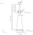
- the distance between the X-ray focal point, which is the divergence point of the X-ray beam, and the detector when the distance becomes the shortest is referred to as the focus-to-detector distance (FDD)
- the distance between the X-ray focal point and the sample when the distance becomes the shortest is referred to as the focus-to-object distance (FOD) (cf. Fig. 5 ).
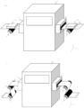
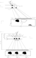
- Figs. 1 and 2 are schematic views showing a schematic configuration for explaining one aspect of an inspection device of the present invention.
- Fig. 1 shows the case of an inline inspection device in which a sample is conveyed in a sheet form
- Fig. 2 shows the case of an inline inspection device for a roll-to-roll continuous film, sheet, or the like.
- the inspection device is equipped with a housing 1.
- the housing 1 includes a carry-in port 3 for a sample to be carried in and a carry-out port 4 for a sample to be carried out.
- each of the housing 1, the carry-in port 3, and the carry-out port 4 is usually equipped with a shielding wall capable of shielding the ionizing radiation, such as lead and stainless steel, on the inner wall, and the opening of the carry-out port 3 is usually equipped with a rubber shielding cover to prevent leakage of ionizing radiation to the outside.
- a sample sample 2(a) and sample 2(b)
- the sample conveyance belt 6 moves with a sample conveyance roll 5 to introduce the sample into the housing.
- the sample 2 is brought into contact with the sample conveyance roll 5 and directly conveyed into the housing 1.
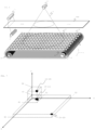
- Fig. 3 is a view schematically showing the inside of Fig. 1
- Fig. 4 is a view schematically showing the inside of Fig. 2
- the conveyed sample sample 2(a) and sample 2(b)
- a thickness measurement sensor 7 that measures the thickness of the sample
- a radiation source 8 that performs irradiation with radiation
- a detector 10 that detects radiation 9 and converts the radiation 9 into an electrical signal
- the thickness measurement sensor 7 is disposed upstream inside the housing 1, immediately after the sample has passed through the carry-in port 3, and measures the thickness of the sample.
- a thickness H of each sample carried in is calculated by measuring the height profile of the sample from the surface of the sample conveyance belt 6 using the thickness measurement sensor 7.
- the thickness measurement sensors 7 are disposed above and below the sample, and the distance between each of the upper and lower measurement sensors and the sample is measured. Assuming that the distance between the upper measurement sensor and the sample 2 is Ht, the distance between the lower measurement sensor and the sample 2 is Hb, and the distance between the upper and lower measurement sensors is Hd, the thickness H of the sample 2 can be calculated as Hd - Ht - Hb.
- the radiation source 8 which is a point light source
- the radiation spreads radially, and the space irradiated with the radiation is usually conical. Due to the radial irradiation, defects located on the side closer to the radiation source 8 in the sample are imaged as large images in the detector 10, and defects located on the farther side are imaged as small images in the detector 10.
- an X-ray source is used as the radiation source 8
- an accessory facility such as a high-voltage generator that supplies high-voltage power to the X-ray tube and an X-ray controller that controls tube voltage and tube current is required, but is not shown in the figure.
- the signal (image information) output from the detector 8 is transmitted to an image processing device that processes the signal, which is then processed by a data processing unit (not shown) to make a quality determination.
- the signal processing unit and the data processing unit can also be housed inside the housing 1.
- the thickness measurement sensor 7 is used to accurately obtain the surface position of the sample.
- a plurality of sensors may be arranged in a direction where an increase in the number of measurement points is desired, or a single sensor capable of measuring multiple points may be used.
- the thickness measurement sensor is installed, for example, at a position upstream of the sample conveyance belt, and measurement is performed sequentially as samples are conveyed.
- a laser triangulation type displacement meter, a laser interferometer, an ultrasonic distance meter, an eddy current type displacement sensor, a stylus type displacement meter, or the like is used as the measuring instrument.
- the laser triangulation type displacement meter is preferable from the viewpoint of being able to perform measurement in a non-contact manner, being less likely to be affected by the material of the inspection object, being easy to realize a response speed and multi-point measurement, and the like.
- a method called a light cutting method is preferable, in which a sample is irradiated with linear light generated by a laser light source or the like, and the trajectory of reflected/scattered light according to the surface shape of the sample is acquired as a height profile.
- the measuring instrument measures the thickness of the sample by reading the position of the trajectory of the light with a light-receiving means such as an image sensor and quantifying the trajectory as the surface shape of the sample surface.
- the radiation source is not particularly limited as long as the radiation source can emit radiation transmittable through a sample, but a radiation source that generates an electromagnetic wave is desirable because handling is simple and high measurement accuracy can be expected, and in particular, an X-ray source is preferably used.
- the X-ray source that can be used is not particularly limited, and a known X-ray source can be used.
- the tube voltage of the X-ray tube is not particularly limited.
- the radiation source may be a radiation source capable of performing irradiation with other types of radiation, such as gamma rays and neutron rays, or electromagnetic waves instead of X-rays, depending on the type of sample, inspection mode, and the like.
- the radiation source performs radial irradiation from a point light source that is a divergence point.
- the detector has a function of detecting radiation emitted from the radiation source and converting the radiation into an electrical signal.
- the element detects the emitted radiation and generates an output according to the detected intensity.
- a detector element of the type described below can be applied: an indirect conversion type detection element that converts X-rays into visible rays using a scintillator and then receives the visible rays with a photodiode to generate an output; or a direct conversion type detection element using a semiconductor such as an amorphous semiconductor (a-Se) or cadmium telluride (CdTe) that converts X-rays directly into an electrical signal to generate an output.
- a-Se amorphous semiconductor
- CdTe cadmium telluride
- a plurality of detectors may be arranged, and examples of the detectors to use include: a line sensor with elements arranged on a straight line; a time delay integration (TDI) sensor; a detector including a light-receiving element such as a charge-coupled device (CCD) image sensor or a complementary metal-oxide-semiconductor (CMOS) image sensor with elements arranged in a planar shape; and a general-purpose two-dimensional X-ray detector flat-panel detector (FPD).
- TDI time delay integration
- CCD charge-coupled device
- CMOS complementary metal-oxide-semiconductor
- FPD general-purpose two-dimensional X-ray detector flat-panel detector
- the indirect conversion type FPD preferably includes a cellular scintillator.
- a scintillator panel is used to convert radiation into visible light.
- the scintillator panel includes a phosphor that emits X-rays such as cesium iodide (CsI).
- CsI cesium iodide
- the phosphor emits visible light according to the emitted X-rays, the emitted light is converted into an electrical signal by a thin film transistor (TFT), a CCD, or a CMOS, and the electrical signal is transferred, whereby X-ray information can be converted into digital image information.
- the FPD employing the adopted cellular scintillator is filled with phosphor in cells partitioned by partition walls, thus making it possible to suppress the effects of visible light scattering.
- the FPD including the cellular scintillator has high sharpness, and can detect minute defects and defect positions with high accuracy. From the viewpoint that a cellular scintillator with a large area and high sharpness can be easily formed, it is further preferable to use a cellular scintillator prepared by processing a partition wall by photolithography using a photosensitive paste.
- the flexible detector can be curved and has flexibility.
- the flexible detector can be obtained by disposing a detection unit with pixels arranged in a matrix on a substrate formed of a bendable flexible resin or the like.
- a photodiode that allows a current corresponding to the total amount of energy of the received electromagnetic wave to flow
- a pixel circuit that controls the driving of the photodiode, and the like are arranged.
- an electrical signal corresponding to the total amount of received energy can be output from each pixel to the control unit.
- the inspection device of the present invention includes a movement mechanism that moves the detector along the direction in which the sample is conveyed by the conveyance mechanism. Including such a movement mechanism as described later enables inspection with high resolution, high sensitivity, and high S/N even at high speed.
- the movement mechanism preferably includes an endless annular conveyance belt, and the detector is disposed on this conveyance belt to perform inspection.
- the power supply cable can be connected to an external power cable with a rotary connector, such as a slip ring, that transmits power from the outside to the rotating body.
- a rotary connector such as a slip ring
- wireless communication can be used.
- the imaging start timing is set for each row of pixels arranged in a direction (X direction) parallel to the conveyance belt surface and perpendicular to the movement direction of the detector, and image acquisition is started at the timing when a row of a certain pixel enters a region irradiated with radiation from the radiation source, and image acquisition is terminated at the timing when the row becomes out of the irradiation range.
- Image data during the image acquisition period is temporarily stored in a storage device provided in the detector, and the image data is transmitted to an external receiver when image acquisition is terminated.
- the timings for the start and end of image acquisition can be known by disposing sensors capable of detecting the passage of the detector upstream and downstream of the irradiation region and detecting the detector.
- the determination means for determining the presence or absence of a defect includes a means (image information acquisition means, image composition means) that is connected to the detector, acquires the image information on the sample from the detector together with movement information on the sample from the conveyance mechanism, detects a defect present in the sample in the irradiation region, and generates a mapping image in which the position of the defect is specified during the time when the sample is in the irradiation region.
- the determination means preferably includes a means for acquiring the information from the thickness measuring instrument and further acquiring information in the sample thickness direction by calculation.
- the determination means includes a defect candidate detection means for calculating a defect candidate from the acquired image, and a means for determining whether the defect candidate corresponds to the defect.
- the signal obtained by converting radiation detected by a detector pixel 11 into an electrical signal is output with the intensity of the detected radiation as a luminance value.
- the luminance value is high (bright) in the pixel with strong detection and the luminance value is small (dark) in the pixel with weak detection.
- the size of the detector pixel 11 is P [mm] and the resolution to be obtained is Re [mm]
- the conveyance speed of the sample is Vw [mm/sec]
- the resolution is increased, the detection pixels are decreased, the magnification factor is increased, and the sample conveyance speed is increased, the time ⁇ required for one imaging becomes shorter, and a detector with a higher scan rate is required.
- P/M ⁇ Vw - Vd
- a continuous sample such as a roll-to-roll sample, can be imaged without interruption.
- a case where defects 15-(1), 15-(2), 15-(3) of different sizes and shapes are in a certain region in the sample, as shown in Fig. 7 will be described as an example.
- the center of gravity of the defect 15-(1) is at coordinates (X1, Y1, Z1)
- the center of gravity of the defect 15-(2) is at coordinates (X2, Y2, Z1)
- the center of gravity of 15-(3) is at coordinates (X1, Y1, Z2).
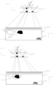
- FIG. 8 to 10 show examples when imaging is continuously performed while the sample and the detector are moved from left to right in the figure (i.e., in the Y axis direction).
- Fig. 8 shows the position of the sample at time point ta and an image at that position
- Fig. 9 shows the position of the sample at time point tb and an image at that position
- Fig. 10 shows the position of the sample at time point tc and an image at that position. Note that ta ⁇ tb ⁇ tc.
- an image corresponding to the defect 15-(1) is shown as 17-(1)
- an image corresponding to the defect 15-(2) is shown as 17-(2)
- an image corresponding to the defect 15-(3) is shown as 17-(3).
- the defects 15-(1), 15-(2) are at the same depth (Z1), and hence the two defects are observed to move while maintaining substantially the same interval in the projection image 16.
- the defects 15-(1), 15-(3) are at different depths (Z1 and Z2), so that the apparent speed of movement in the Y direction differs in the projection image 16, and even if the X and Y coordinates are the same, separated images are obtained with the lapse of a certain time. That is, the movement amount in the projection image (projection movement amount) varies depending on the depth of the defect in the sample.
- Fig. 11 shows the defect 15-(1) and its corresponding image 17-(1) extracted at each time point ta, tb, tc.
- the movement amount Dab [mm] of the defect 15-(1) from time ta to time tb is Vw(tb - ta); the movement amount Dbc [mm] of the defect 15-(1) from time tb to time tc is Vw(tc - tb); the movement amount of the image of the defect from time ta to time tb in the corresponding image is Lab; and the movement amount of the image of the defect from time tb to time tc is Lbc.
- Mz1 FDD/(FOD-Z1), which is a magnification factor Mz1 considering the depth in the sample of the defect 15-(1),is used
- the images at other acquisition times are shifted by the movement amount of the defects and superimposed with the image at a certain time as the center.
- images of defects present at a depth of interest overlap each other, making it possible to obtain a large signal intensity and detect even low-contrast defects.
- Fig. 12 when the image at time point ta (16 in Fig. 8 ) is shifted by -Lab and the image at time point tc (16 in Fig. 10 ) is shifted by +Lbc using the movement amounts Lab, Lbc of the images of the defects calculated at the depth Z1 around the image at time point tb (16 in Fig.
- the defects 15-(1), 15-(2) present at the depth Z1 overlap each other, resulting in a large signal.
- the defect 15-(3) not present at the depth Z1 has different coordinates because of the different apparent movement speed, and does not have a large signal intensity due to overlap. Therefore, similarly to the above method, when the movement amount of the defect relative to Z2 is calculated, followed by shifting by the movement amount and addition, the positions of the defect 15-(3) present at the depth Z2 can be superimposed, resulting in a large signal intensity.
- defect present at each depth can be extracted.
- the defects are detected as one defect, but it is also possible to separate the defects and extract the defects.
- Defect candidates are extracted from a composite image obtained by the above image composition method, and a defect is detected using a luminance threshold in a bright direction and a luminance threshold in a dark direction, which can separate the defect candidate from a portion other than the defect candidate.
- the region satisfying the threshold may be narrowed down by the size of the detection region or may be narrowed down by the feature value of the detection shape. For example, if it is known that the defective foreign matter has an elongated shape in a specific direction due to a certain process, the direction (angle) of the detected shape and its thinness (aspect ratio) may be narrowed down as the feature value.
- a spatial filter or the like may be used prior to detection at the luminance threshold. The defect determination is performed by these methods.
- a cylinder made of SUS304 with a diameter of 50 um and a height of 50 um was bonded as a foreign matter equivalent 18 to a commercially available polyethylene terephthalate film using an epoxy resin, with the bottom surface (or upper surface) as a bonding surface, to obtain an inspection object (manufactured by Toray Precision Co., Ltd.).
- Fig. 13 shows a top image of the inspection object.
- two wires (markers 19) made of SUS304 with a diameter of 200 um were arranged so that the arrangement place of the foreign matter equivalent could be seen.
- X-ray imaging was performed by installing a commercially available X-ray tube (L9181-02, manufactured by Hamamatsu Photonics K.K.), a commercially available X-ray TDI camera (C12300-121, manufactured by Hamamatsu Photonics K.K.), a commercially available linear stage 1 (LEFB32T-1200-S5C5183, manufactured by SMC Corporation) for conveying an inspection object, and a commercially available linear stage 2 (L40B1150-N2-KM02 X-MCC2-KX14B, manufactured by Zaber Technologies Inc.) for conveying an X-ray TDI camera.
- the X-ray tube, the X-ray TDI camera, the linear stage 1, and the linear stage 2 were installed so that a distance FDD from the focal point of the X-ray tube to the X-ray TDI camera was 325 mm and a distance FOD from the focal point of the X-ray tube to the inspection object was 95 mm (cf. Fig. 5 ). Note that the conveyance directions of the linear stage 1 and the linear stage 2 are the same.
- the inspection object was placed on the linear stage 1, and the X-ray TDI camera was placed on the linear stage 2.
- the X-ray tube was irradiated with X-rays at a tube voltage of 40 kV and a tube current of 75 ⁇ A.
- Vw of the linear stage 1 and Vd of the linear stage 2 under conditions described in Table 1, the respective stages were operated and images were captured by an X-ray TDI camera.
- a minimum luminance So of a portion where the foreign matter equivalent was captured, an average luminance Sb of a portion where the foreign matter equivalent was not captured, and a standard deviation ⁇ b of the luminance of the portion where the foreign matter equivalent was not captured were measured.
- Sb and ⁇ b were measured from arbitrarily selected 400 pixels in the image, excluding the place where the foreign matter equivalent was placed and its vicinity (20 pixels square (approximately 280 um x 280 um in this example).
- the luminance was captured by an X-ray TDI camera, and the amount of signal of the output X-ray image was used.
- Table 1 shows the results for the contrast-to-noise ratio (CNR), which is a value obtained by dividing the contrast C, the absolute value of the difference between So and Sb, by ⁇ b.
- CNR contrast-to-noise ratio
- the transmission image is acquired while the detector is moved in the same direction as the movement direction of the sample, a projection image with high temporal resolution can be obtained even with a detector at a low scan rate.
- Images captured at various irradiation angles from the point light source are acquired at a plurality of positions, whereby even when a plurality of defects overlap in a linear shape connecting the radiation source and the detector, the defects can be separated and extracted.
- even a low-contrast defect can be inspected as a large signal from a plurality of images at high speed and with high accuracy.
Landscapes
- Physics & Mathematics (AREA)
- General Physics & Mathematics (AREA)
- Health & Medical Sciences (AREA)
- Life Sciences & Earth Sciences (AREA)
- Immunology (AREA)
- Chemical & Material Sciences (AREA)
- Analytical Chemistry (AREA)
- Biochemistry (AREA)
- General Health & Medical Sciences (AREA)
- Pathology (AREA)
- Molecular Biology (AREA)
- Spectroscopy & Molecular Physics (AREA)
- High Energy & Nuclear Physics (AREA)
- Toxicology (AREA)
- Electromagnetism (AREA)
- Analysing Materials By The Use Of Radiation (AREA)
Applications Claiming Priority (2)
| Application Number | Priority Date | Filing Date | Title |
|---|---|---|---|
| JP2022058034 | 2022-03-31 | ||
| PCT/JP2023/007539 WO2023189135A1 (fr) | 2022-03-31 | 2023-03-01 | Dispositif et procédé d'inspection |
Publications (2)
| Publication Number | Publication Date |
|---|---|
| EP4471411A1 true EP4471411A1 (fr) | 2024-12-04 |
| EP4471411A4 EP4471411A4 (fr) | 2025-07-30 |
Family
ID=88201127
Family Applications (1)
| Application Number | Title | Priority Date | Filing Date |
|---|---|---|---|
| EP23779165.2A Pending EP4471411A4 (fr) | 2022-03-31 | 2023-03-01 | Dispositif et procédé d'inspection |
Country Status (6)
| Country | Link |
|---|---|
| US (1) | US20250224348A1 (fr) |
| EP (1) | EP4471411A4 (fr) |
| JP (1) | JPWO2023189135A1 (fr) |
| KR (1) | KR20240169596A (fr) |
| CN (1) | CN119013552A (fr) |
| WO (1) | WO2023189135A1 (fr) |
Families Citing this family (1)
| Publication number | Priority date | Publication date | Assignee | Title |
|---|---|---|---|---|
| US12590910B2 (en) * | 2023-03-31 | 2026-03-31 | Anritsu Corporation | X-ray inspection apparatus and x-ray inspection system |
Family Cites Families (18)
| Publication number | Priority date | Publication date | Assignee | Title |
|---|---|---|---|---|
| JP2000221144A (ja) * | 1999-02-01 | 2000-08-11 | Sekisui Chem Co Ltd | 透明フィルムの異物検査装置 |
| JP2006258781A (ja) * | 2005-02-15 | 2006-09-28 | Takashima Giken Kk | 異物検査方法及び異物検査装置 |
| JP2008157821A (ja) * | 2006-12-25 | 2008-07-10 | Matsushita Electric Works Ltd | X線異物検査装置 |
| JP5467830B2 (ja) * | 2009-09-18 | 2014-04-09 | 浜松ホトニクス株式会社 | 放射線検出装置 |
| JP5569061B2 (ja) * | 2010-03-15 | 2014-08-13 | オムロン株式会社 | X線検査方法、x線検査装置およびx線検査プログラム |
| JP5555048B2 (ja) * | 2010-05-21 | 2014-07-23 | アンリツ産機システム株式会社 | X線検査装置 |
| JP5853781B2 (ja) * | 2012-03-15 | 2016-02-09 | オムロン株式会社 | X線検査装置、x線検査のための撮像方法 |
| JP2014085252A (ja) * | 2012-10-24 | 2014-05-12 | Toyota Motor Corp | フィルム検査方法 |
| JP5903392B2 (ja) * | 2013-02-07 | 2016-04-13 | 株式会社日立ビルシステム | 乗客コンベアの移動手摺り探傷装置 |
| JP6355247B2 (ja) | 2013-08-29 | 2018-07-11 | 株式会社イシダ | 透過光検査装置 |
| JP6512980B2 (ja) * | 2015-07-29 | 2019-05-15 | 株式会社日立ハイテクサイエンス | X線透過検査装置及びx線透過検査方法 |
| JP6625470B2 (ja) * | 2016-03-30 | 2019-12-25 | アンリツインフィビス株式会社 | 異物検出装置および異物検出方法 |
| JP6738363B2 (ja) * | 2018-03-09 | 2020-08-12 | 浜松ホトニクス株式会社 | 画像取得システムおよび画像取得方法 |
| CN111684269B (zh) * | 2018-03-15 | 2022-12-30 | 东丽株式会社 | 异物的检查方法、检查装置、薄膜辊以及薄膜辊的制造方法 |
| WO2020004435A1 (fr) * | 2018-06-27 | 2020-01-02 | 東レ株式会社 | Méthode et dispositif d'inspection de transmission de rayonnement et méthode de fabrication de film microporeux |
| JP7209329B2 (ja) | 2018-06-28 | 2023-01-20 | 株式会社 システムスクエア | 検査装置 |
| JP7201481B2 (ja) | 2019-03-04 | 2023-01-10 | 株式会社日立ハイテクサイエンス | X線検査装置及びx線検査方法 |
| JP6766216B1 (ja) * | 2019-04-24 | 2020-10-07 | Ckd株式会社 | 検査装置、包装シート製造装置及び包装シート製造方法 |
-
2023
- 2023-03-01 US US18/850,349 patent/US20250224348A1/en active Pending
- 2023-03-01 JP JP2023515104A patent/JPWO2023189135A1/ja active Pending
- 2023-03-01 EP EP23779165.2A patent/EP4471411A4/fr active Pending
- 2023-03-01 KR KR1020247024350A patent/KR20240169596A/ko active Pending
- 2023-03-01 CN CN202380030743.0A patent/CN119013552A/zh active Pending
- 2023-03-01 WO PCT/JP2023/007539 patent/WO2023189135A1/fr not_active Ceased
Also Published As
| Publication number | Publication date |
|---|---|
| KR20240169596A (ko) | 2024-12-03 |
| JPWO2023189135A1 (fr) | 2023-10-05 |
| WO2023189135A1 (fr) | 2023-10-05 |
| CN119013552A (zh) | 2024-11-22 |
| US20250224348A1 (en) | 2025-07-10 |
| EP4471411A4 (fr) | 2025-07-30 |
Similar Documents
| Publication | Publication Date | Title |
|---|---|---|
| US7236564B2 (en) | Linear array detector system and inspection method | |
| US10054555B2 (en) | X-ray transmission inspection apparatus and inspection method using the same | |
| JP5555048B2 (ja) | X線検査装置 | |
| EP3348997A1 (fr) | Procédé d'inspection par rayons x et dispositif d'inspection par rayons x | |
| US20160041110A1 (en) | X-ray transmission inspection apparatus and extraneous substance detecting method | |
| KR20080022089A (ko) | X선-단층촬영 및/또는 저선량단층촬영 장치 | |
| KR20130016081A (ko) | 투과 x선 분석 장치 및 방법 | |
| US10989674B2 (en) | X-ray inspection apparatus and x-ray inspection method | |
| US20120049074A1 (en) | Detector array with pre-focused anti-scatter grid | |
| EP4471411A1 (fr) | Dispositif et procédé d'inspection | |
| US20250139755A1 (en) | Unevenness measuring device for sheet-shaped material, and unevenness measuring method for sheet-shaped material | |
| KR20150113819A (ko) | X선 투과 검사 장치 | |
| JP6506629B2 (ja) | X線受光装置およびこれを備えたx線検査装置 | |
| JP6450075B2 (ja) | X線検査装置 | |
| JP5620801B2 (ja) | X線異物検出装置 | |
| JP7724238B2 (ja) | 撮像ユニット及び撮像システム | |
| WO2023017664A1 (fr) | Détecteur de rayonnement | |
| CN107727671A (zh) | 一种压力管道射线数字成像未焊透检测系统 | |
| JP7582507B2 (ja) | X線検査装置及びx線検査方法 | |
| JP2015200620A (ja) | X線検査装置 | |
| JP6401504B2 (ja) | X線検査装置 | |
| US20260009743A1 (en) | X-ray inspection device and x-ray inspection method | |
| JP5759332B2 (ja) | X線異物検出装置 | |
| KR20250103266A (ko) | 방사능 오염물질 검출 시스템 및 그 동작방법 |
Legal Events
| Date | Code | Title | Description |
|---|---|---|---|
| STAA | Information on the status of an ep patent application or granted ep patent |
Free format text: STATUS: THE INTERNATIONAL PUBLICATION HAS BEEN MADE |
|
| PUAI | Public reference made under article 153(3) epc to a published international application that has entered the european phase |
Free format text: ORIGINAL CODE: 0009012 |
|
| STAA | Information on the status of an ep patent application or granted ep patent |
Free format text: STATUS: REQUEST FOR EXAMINATION WAS MADE |
|
| 17P | Request for examination filed |
Effective date: 20240829 |
|
| AK | Designated contracting states |
Kind code of ref document: A1 Designated state(s): AL AT BE BG CH CY CZ DE DK EE ES FI FR GB GR HR HU IE IS IT LI LT LU LV MC ME MK MT NL NO PL PT RO RS SE SI SK SM TR |
|
| DAV | Request for validation of the european patent (deleted) | ||
| DAX | Request for extension of the european patent (deleted) | ||
| A4 | Supplementary search report drawn up and despatched |
Effective date: 20250627 |
|
| RIC1 | Information provided on ipc code assigned before grant |
Ipc: G01N 23/04 20180101AFI20250623BHEP Ipc: G01N 23/044 20180101ALI20250623BHEP Ipc: G01N 23/18 20180101ALI20250623BHEP |