EP4471435A2 - Aiguille de test, sonde de test et testeur à doigt pour tester les circuits imprimés - Google Patents
Aiguille de test, sonde de test et testeur à doigt pour tester les circuits imprimés Download PDFInfo
- Publication number
- EP4471435A2 EP4471435A2 EP24199871.5A EP24199871A EP4471435A2 EP 4471435 A2 EP4471435 A2 EP 4471435A2 EP 24199871 A EP24199871 A EP 24199871A EP 4471435 A2 EP4471435 A2 EP 4471435A2
- Authority
- EP
- European Patent Office
- Prior art keywords
- test
- measuring
- test needle
- electrical
- electrically conductive
- Prior art date
- Legal status (The legal status is an assumption and is not a legal conclusion. Google has not performed a legal analysis and makes no representation as to the accuracy of the status listed.)
- Pending
Links
Images


Classifications
-
- G—PHYSICS
- G01—MEASURING; TESTING
- G01R—MEASURING ELECTRIC VARIABLES; MEASURING MAGNETIC VARIABLES
- G01R1/00—Details of instruments or arrangements of the types included in groups G01R5/00 - G01R13/00 and G01R31/00
- G01R1/02—General constructional details
- G01R1/06—Measuring leads; Measuring probes
- G01R1/067—Measuring probes
- G01R1/06711—Probe needles; Cantilever beams; "Bump" contacts; Replaceable probe pins
- G01R1/06716—Elastic
-
- G—PHYSICS
- G01—MEASURING; TESTING
- G01R—MEASURING ELECTRIC VARIABLES; MEASURING MAGNETIC VARIABLES
- G01R31/00—Arrangements for testing electric properties; Arrangements for locating electric faults; Arrangements for electrical testing characterised by what is being tested not provided for elsewhere
- G01R31/28—Testing of electronic circuits, e.g. by signal tracer
- G01R31/302—Contactless testing
- G01R31/312—Contactless testing by capacitive methods
-
- G—PHYSICS
- G01—MEASURING; TESTING
- G01R—MEASURING ELECTRIC VARIABLES; MEASURING MAGNETIC VARIABLES
- G01R1/00—Details of instruments or arrangements of the types included in groups G01R5/00 - G01R13/00 and G01R31/00
- G01R1/02—General constructional details
- G01R1/06—Measuring leads; Measuring probes
- G01R1/067—Measuring probes
- G01R1/06711—Probe needles; Cantilever beams; "Bump" contacts; Replaceable probe pins
- G01R1/06733—Geometry aspects
-
- G—PHYSICS
- G01—MEASURING; TESTING
- G01B—MEASURING LENGTH, THICKNESS OR SIMILAR LINEAR DIMENSIONS; MEASURING ANGLES; MEASURING AREAS; MEASURING IRREGULARITIES OF SURFACES OR CONTOURS
- G01B21/00—Measuring arrangements or details thereof, where the measuring technique is not covered by the other groups of this subclass, unspecified or not relevant
- G01B21/22—Measuring arrangements or details thereof, where the measuring technique is not covered by the other groups of this subclass, unspecified or not relevant for measuring angles or tapers; for testing the alignment of axes
-
- G—PHYSICS
- G01—MEASURING; TESTING
- G01L—MEASURING FORCE, STRESS, TORQUE, WORK, MECHANICAL POWER, MECHANICAL EFFICIENCY, OR FLUID PRESSURE
- G01L5/00—Apparatus for, or methods of, measuring force, work, mechanical power, or torque, specially adapted for specific purposes
- G01L5/0057—Apparatus for, or methods of, measuring force, work, mechanical power, or torque, specially adapted for specific purposes measuring forces due to spring-shaped elements
-
- G—PHYSICS
- G01—MEASURING; TESTING
- G01R—MEASURING ELECTRIC VARIABLES; MEASURING MAGNETIC VARIABLES
- G01R1/00—Details of instruments or arrangements of the types included in groups G01R5/00 - G01R13/00 and G01R31/00
- G01R1/02—General constructional details
- G01R1/04—Housings; Supporting members; Arrangements of terminals
- G01R1/0408—Test fixtures or contact fields; Connectors or connecting adaptors; Test clips; Test sockets
-
- G—PHYSICS
- G01—MEASURING; TESTING
- G01R—MEASURING ELECTRIC VARIABLES; MEASURING MAGNETIC VARIABLES
- G01R1/00—Details of instruments or arrangements of the types included in groups G01R5/00 - G01R13/00 and G01R31/00
- G01R1/02—General constructional details
- G01R1/06—Measuring leads; Measuring probes
- G01R1/067—Measuring probes
- G01R1/06711—Probe needles; Cantilever beams; "Bump" contacts; Replaceable probe pins
- G01R1/06716—Elastic
- G01R1/06722—Spring-loaded
-
- G—PHYSICS
- G01—MEASURING; TESTING
- G01R—MEASURING ELECTRIC VARIABLES; MEASURING MAGNETIC VARIABLES
- G01R1/00—Details of instruments or arrangements of the types included in groups G01R5/00 - G01R13/00 and G01R31/00
- G01R1/02—General constructional details
- G01R1/06—Measuring leads; Measuring probes
- G01R1/067—Measuring probes
- G01R1/06711—Probe needles; Cantilever beams; "Bump" contacts; Replaceable probe pins
- G01R1/06733—Geometry aspects
- G01R1/06738—Geometry aspects related to tip portion
-
- G—PHYSICS
- G01—MEASURING; TESTING
- G01R—MEASURING ELECTRIC VARIABLES; MEASURING MAGNETIC VARIABLES
- G01R1/00—Details of instruments or arrangements of the types included in groups G01R5/00 - G01R13/00 and G01R31/00
- G01R1/02—General constructional details
- G01R1/06—Measuring leads; Measuring probes
- G01R1/067—Measuring probes
- G01R1/06711—Probe needles; Cantilever beams; "Bump" contacts; Replaceable probe pins
- G01R1/06733—Geometry aspects
- G01R1/06744—Microprobes, i.e. having dimensions as IC details
-
- G—PHYSICS
- G01—MEASURING; TESTING
- G01R—MEASURING ELECTRIC VARIABLES; MEASURING MAGNETIC VARIABLES
- G01R1/00—Details of instruments or arrangements of the types included in groups G01R5/00 - G01R13/00 and G01R31/00
- G01R1/02—General constructional details
- G01R1/06—Measuring leads; Measuring probes
- G01R1/067—Measuring probes
- G01R1/06711—Probe needles; Cantilever beams; "Bump" contacts; Replaceable probe pins
- G01R1/06755—Material aspects
- G01R1/06761—Material aspects related to layers
-
- G—PHYSICS
- G01—MEASURING; TESTING
- G01R—MEASURING ELECTRIC VARIABLES; MEASURING MAGNETIC VARIABLES
- G01R1/00—Details of instruments or arrangements of the types included in groups G01R5/00 - G01R13/00 and G01R31/00
- G01R1/02—General constructional details
- G01R1/06—Measuring leads; Measuring probes
- G01R1/067—Measuring probes
- G01R1/07—Non contact-making probes
-
- G—PHYSICS
- G01—MEASURING; TESTING
- G01R—MEASURING ELECTRIC VARIABLES; MEASURING MAGNETIC VARIABLES
- G01R1/00—Details of instruments or arrangements of the types included in groups G01R5/00 - G01R13/00 and G01R31/00
- G01R1/02—General constructional details
- G01R1/06—Measuring leads; Measuring probes
- G01R1/067—Measuring probes
- G01R1/073—Multiple probes
- G01R1/07307—Multiple probes with individual probe elements, e.g. needles, cantilever beams or bump contacts, fixed in relation to each other, e.g. bed of nails fixture or probe card
- G01R1/07314—Multiple probes with individual probe elements, e.g. needles, cantilever beams or bump contacts, fixed in relation to each other, e.g. bed of nails fixture or probe card the body of the probe being perpendicular to test object, e.g. bed of nails or probe with bump contacts on a rigid support
- G01R1/07328—Multiple probes with individual probe elements, e.g. needles, cantilever beams or bump contacts, fixed in relation to each other, e.g. bed of nails fixture or probe card the body of the probe being perpendicular to test object, e.g. bed of nails or probe with bump contacts on a rigid support for testing printed circuit boards
-
- G—PHYSICS
- G01—MEASURING; TESTING
- G01R—MEASURING ELECTRIC VARIABLES; MEASURING MAGNETIC VARIABLES
- G01R1/00—Details of instruments or arrangements of the types included in groups G01R5/00 - G01R13/00 and G01R31/00
- G01R1/02—General constructional details
- G01R1/06—Measuring leads; Measuring probes
- G01R1/067—Measuring probes
- G01R1/073—Multiple probes
- G01R1/07392—Multiple probes manipulating each probe element or tip individually
-
- G—PHYSICS
- G01—MEASURING; TESTING
- G01R—MEASURING ELECTRIC VARIABLES; MEASURING MAGNETIC VARIABLES
- G01R23/00—Arrangements for measuring frequencies; Arrangements for analysing frequency spectra
- G01R23/02—Arrangements for measuring frequency, e.g. pulse repetition rate; Arrangements for measuring period of current or voltage
-
- G—PHYSICS
- G01—MEASURING; TESTING
- G01R—MEASURING ELECTRIC VARIABLES; MEASURING MAGNETIC VARIABLES
- G01R27/00—Arrangements for measuring resistance, reactance, impedance, or electric characteristics derived therefrom
- G01R27/02—Measuring real or complex resistance, reactance, impedance, or other two-pole characteristics derived therefrom, e.g. time constant
- G01R27/26—Measuring inductance or capacitance; Measuring quality factor, e.g. by using the resonance method; Measuring loss factor; Measuring dielectric constants ; Measuring impedance or related variables
- G01R27/2605—Measuring capacitance
-
- G—PHYSICS
- G01—MEASURING; TESTING
- G01R—MEASURING ELECTRIC VARIABLES; MEASURING MAGNETIC VARIABLES
- G01R31/00—Arrangements for testing electric properties; Arrangements for locating electric faults; Arrangements for electrical testing characterised by what is being tested not provided for elsewhere
- G01R31/28—Testing of electronic circuits, e.g. by signal tracer
- G01R31/2801—Testing of printed circuits, backplanes, motherboards, hybrid circuits or carriers for multichip packages [MCP]
- G01R31/281—Specific types of tests or tests for a specific type of fault, e.g. thermal mapping, shorts testing
- G01R31/2813—Checking the presence, location, orientation or value, e.g. resistance, of components or conductors
-
- G—PHYSICS
- G01—MEASURING; TESTING
- G01R—MEASURING ELECTRIC VARIABLES; MEASURING MAGNETIC VARIABLES
- G01R31/00—Arrangements for testing electric properties; Arrangements for locating electric faults; Arrangements for electrical testing characterised by what is being tested not provided for elsewhere
- G01R31/28—Testing of electronic circuits, e.g. by signal tracer
- G01R31/2851—Testing of integrated circuits [IC]
- G01R31/2855—Environmental, reliability or burn-in testing
- G01R31/286—External aspects, e.g. related to chambers, contacting devices or handlers
- G01R31/2863—Contacting devices, e.g. sockets, burn-in boards or mounting fixtures
-
- G—PHYSICS
- G01—MEASURING; TESTING
- G01R—MEASURING ELECTRIC VARIABLES; MEASURING MAGNETIC VARIABLES
- G01R31/00—Arrangements for testing electric properties; Arrangements for locating electric faults; Arrangements for electrical testing characterised by what is being tested not provided for elsewhere
- G01R31/28—Testing of electronic circuits, e.g. by signal tracer
- G01R31/2851—Testing of integrated circuits [IC]
- G01R31/2886—Features relating to contacting the IC under test, e.g. probe heads; chucks
-
- G—PHYSICS
- G01—MEASURING; TESTING
- G01R—MEASURING ELECTRIC VARIABLES; MEASURING MAGNETIC VARIABLES
- G01R31/00—Arrangements for testing electric properties; Arrangements for locating electric faults; Arrangements for electrical testing characterised by what is being tested not provided for elsewhere
- G01R31/28—Testing of electronic circuits, e.g. by signal tracer
- G01R31/2851—Testing of integrated circuits [IC]
- G01R31/2886—Features relating to contacting the IC under test, e.g. probe heads; chucks
- G01R31/2887—Features relating to contacting the IC under test, e.g. probe heads; chucks involving moving the probe head or the IC under test; docking stations
-
- G—PHYSICS
- G01—MEASURING; TESTING
- G01R—MEASURING ELECTRIC VARIABLES; MEASURING MAGNETIC VARIABLES
- G01R31/00—Arrangements for testing electric properties; Arrangements for locating electric faults; Arrangements for electrical testing characterised by what is being tested not provided for elsewhere
- G01R31/28—Testing of electronic circuits, e.g. by signal tracer
- G01R31/2851—Testing of integrated circuits [IC]
- G01R31/2893—Handling, conveying or loading, e.g. belts, boats, vacuum fingers
Definitions
- the present invention relates to a test needle for measuring electrically conductive layers in holes in printed circuit boards, as well as a test probe with such a test needle and a finger tester for testing printed circuit boards with such a test needle or with such a test probe.
- the boards are often initially produced with so-called coupons.
- the coupons are areas of the board that have predetermined conductive paths in order to carry out measurements on them. After the measurements have been carried out to test whether the board has been manufactured correctly, the coupons are separated from the rest of the board. The remaining board forms one or more so-called panels, which are equipped with electrical components and used in electrical products.
- the coupons have special conductor tracks, which can be used to easily determine whether the production process meets the requirements for producing high-frequency conductor tracks, for example. Furthermore, stress tests can be carried out on the coupon's conductor tracks, which can also destroy individual conductor tracks on the coupons. Since the coupon's conductor tracks are not used in later products, they can be specially optimized for certain test processes.
- This device has a capacitive probe, which is inserted into a back drilled hole in a circuit board. The capacitance of the capacitive probe is measured. Any electrically conductive material still present in the back drilled hole is detected based on the capacitance. This can detect errors during back drilling.
- the present invention is based on the object of providing a test needle for measuring electrically conductive layers in holes in printed circuit boards and a corresponding To create a test probe and a finger tester with which a drilled hole in a printed circuit board can be easily, reliably and very precisely tested in accordance with the US 9,341,670 B2 described method can be measured.
- a test needle according to the invention for measuring electrically conductive layers in holes in printed circuit boards comprises an electrical conductor which is surrounded by a shield, wherein the test needle has a connection end at which it can be electrically connected to a capacitive measuring device and a measuring end which can be inserted into a hole during a measurement.
- This test needle is characterized by the fact that a capacitive measuring body connected to the electrical conductor is arranged outside the shield at the measuring end, which can form a capacitive coupling with an electrically conductive layer in the bore.
- the test needle can be used to very precisely determine the location of the capacitive measuring body based on the measured capacitance in relation to an electrically conductive layer.
- the measuring body is preferably surrounded by an electrical insulation layer so that no electrical contact can occur between the measuring body and another electrically conductive body.
- the measuring body can be designed in the form of a hollow cylinder.
- the measuring body can also be formed by one or more turns of the electrical conductor, whereby these turns are located outside the shield.
- the measuring body preferably has a maximum diameter of 1.5 mm, in particular a maximum diameter of 1 mm, and preferably a maximum diameter of 0.75 mm.
- the measuring body preferably has a maximum length of 0.5 mm in the axial direction of the test needle, preferably a maximum length of 0.25 mm and in particular a maximum length of 0.15 mm.
- the test needle can have an electrically conductive tube that forms the shield, in which a cable that includes the electrical conductor and an electrical insulation layer is guided.
- the cable can protrude a little from the tube at the connection end in order to be connected to the capacitive measuring device. At the measuring end, the cable can protrude a little in order to be arranged around the tube in one or more turns to form the measuring body. This is a very simple construction of the test needle, but it allows very precise measurements.
- the cable is preferably wound with two, three, four or more turns around the electrically conductive tube to form the measuring body.
- a test probe for measuring electrically conductive layers in holes in printed circuit boards can be provided with a test needle as described above and has a touch sensor with which it can be determined whether the test needle is touching another body.
- the touch sensor can be used to measure the depth of a blind hole by touching the test probe once on the surface of the circuit board to be tested and another time on the bottom of the blind hole and detecting the respective contact and recording the position of the test probe. The difference between the two positions gives the depth of the blind hole.
- the actual capacitive measurement should be carried out as contact-free as possible, which is why the touch sensor can also be used to try to determine whether there is contact with another body and then, if necessary, to move the test needle so that it no longer touches the body.
- the touch sensor may include a spring-elastic holder for holding the test needle and a sensor for detecting a deflection of the spring-elastic holder.
- the sensor for detecting a deflection of the spring-elastic holder can be an optical sensor.
- This optical sensor can be designed in different ways.
- a light source can be arranged on the spring-elastic holder directly or indirectly via a light guide, with the light output being detected by an optical sensor.
- the light cone is moved away from the optical sensor, which can be detected by a different brightness. It is also possible to provide a light barrier.
- a stop can be formed on the test probe, against which the test needle and/or the spring-elastic holder rests in the non-deflected state. This clearly defines the position of the test needle in the non-deflected state with respect to the test probe. If the position of the test probe is known, the position of the test needle and thus the position of the measuring body can also be derived from this.
- a finger tester for testing printed circuit boards in particular for testing unpopulated printed circuit boards, preferably has a test finger which is freely movable in a predetermined test area in order to be movable into the vicinity of a predetermined contact point of the printed circuit board.
- the test finger can be provided with a test needle as explained above or with a test probe as explained above.
- the finger tester can have several test fingers, wherein one or more of the further test fingers are designed with a test needle for electrically contacting predetermined contact points of the circuit board.
- the invention relates to a method for measuring electrically conductive layers in holes in printed circuit boards.
- a test needle or a test probe or the finger tester explained above is used.
- the test needle is inserted into a hole with the capacitive measuring body.
- the location of the capacitive measuring body is recorded and at the same time the electrical capacitance of the capacitive measuring body to its surroundings is measured.
- the measured capacitance is used to determine whether there is an electrical conductor near the recorded location.
- This capacitive measuring body can also be inserted into small holes, so that electrically conductive layers formed on the inner surface can be reliably detected.
- the depth of a blind hole to be measured can also be determined using the touch sensor explained above. This determination of the depth can be carried out before, during or after the capacitive measurement.
- an electrical signal with a frequency of at least 1 kHz is applied. Higher frequencies of, for example, at least 2 kHz or at least 4 kHz can also be used.
- the measurement signal can be applied to the conductor of the test needle and thus to the capacitive measuring body.
- the measurement signal induced on a conductor track that is to be connected to a section of an electrical conductor that is to be measured is scanned.
- the measurement signal is applied to a conductor track that is to be connected to the electrical conductor that is scanned by the capacitive measuring body.
- the measurement signal from this electrical conductor is then induced on the capacitive measuring body and can be recorded and evaluated accordingly by the measuring device. This is particularly useful if the electrical conductor is connected to many electrically conductive sections that are located in different holes. A test finger then has to be placed on this electrical conductor just once and the test probe can scan the electrical conductors located in several holes in succession.
- a comparison can be made with a capacitance profile of a properly formed bore.
- a "properly formed bore” is a bore in which desired areas of the inner surface are provided with an electrically conductive layer that is connected to the electrical conductor to which the measuring signal is applied and other areas of the inner surface of the bore are not provided with an electrically conductive layer. The arrangement of the electrically conductive layer on the inner surface of the bore can thus be determined from the comparison. If the measured capacitance profile matches the specified capacitance profile, then the bore is properly formed, i.e. that an electrically conductive layer is provided only at the desired locations. If there are deviations, however, then this means that either an electrically conductive layer is missing at a certain location or an electrically conductive layer is provided at a certain location where no electrically conductive layer should be provided.
- test needle is always held as perpendicular as possible to the surface of the circuit board to be tested, since the holes are usually drilled perpendicular to the surface of the circuit board. This means that the test needle is aligned axially to the respective hole and the risk of collision with the inner surface of a hole is low.
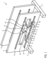
- the invention can be carried out by means of a finger tester 1 which has several test fingers 2, each of which is provided with a test probe 3, with which a circuit board 4 to be tested can be electrically contacted in order to feed in or tap off a corresponding measuring signal in the conductor tracks ( Figure 1 ).
- test probes 3 are used, for example, in the WO 03/048787 A1 described, to which reference is made in this regard.
- the finger tester has two traverse units 5, on which several guide rails 6 are arranged, which extend over a test area extend in which the circuit board 4 to be tested can be accommodated.
- Each traverse unit 5 forms a frame with an elongated through-opening.
- the two traverse units 5 stand vertically on a holder 7 so that their through-openings are aligned.
- the test area for accommodating the circuit board 4 extends through the through-openings of the traverse units 5.
- each traverse unit has four guide rails 6, two of which are arranged on each side of the traverse unit 5. On each side of the traverse unit, one of the guide rails 6 is located above and the other of the guide rails is located below the through-opening 8.
- At least one carriage 9 is movably arranged on each guide rail 6, which carries one of the test fingers 2.
- two carriages 9 are provided on each guide rail 6. In principle, however, more than two carriages 9 can also be arranged on a guide rail 6.
- test fingers 2 are pivotably attached to the slide 9 at one end.
- a structure of a finger tester is shown, for example, in WO 2014/140029 A1 In this regard, reference is made to this document in its entirety.
- test probes 3 are arranged at the ends remote from the carriages 9, the free ends of the test fingers 2, and each have a test needle 10, which is directed with a contact tip 11 in the direction of the circuit board 4 to be contacted.
- the test fingers 2 can be moved with the test probes 3 in the direction of the circuit board 4 and away from the circuit board 4 in order to arrange the contact tip 11 either on the surface of the circuit board or to insert it into a hole in the circuit board 4.
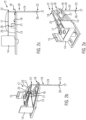
- test fingers 2 or several of the test fingers 2 each have a test probe 12 ( Figure 2a-2c ), which is designed for contact-free, capacitive scanning of holes and in particular blind holes in the circuit board 4.
- a test probe 12 has a base plate 13, which is designed as a circuit board.
- a locking body 14 is arranged on the base plate 13, which has two locking arms 15, with which the test probe 12 can be fixed to one of the test fingers 2 in a locking manner.
- Two spring arms 16, 17 are attached to the locking body 14.
- One of the two spring arms lies directly on the base plate 13 and is clamped between the base plate 13 and the locking body 14.
- the other spring arm 17 is attached to the surface of the locking body 14 remote from the base plate 13 by means of two screws.
- the spring arms 16, 17 are arranged parallel to one another. Starting from the locking body 14, the base plate 13 and the spring arms 16, 17 taper in plan view to a free end 18, at which the two spring arms 16, 17 each protrude a little. At these ends of the A test needle 19 is attached to each of the spring arms 16, 17, so that the elastic spring arms 16, 17, the locking body 14 and the section of the test needle 19 connecting the two spring arms 16, 17 form a parallelogram.
- the two spring arms 16, 17 can be pivoted away from the base plate 13 with their free ends, so that the test needle is elastically mounted on the test probe 12.
- the spring arm 16 directly on the base plate is referred to below as the base spring arm 16 and the spring arm 17 remote from the base plate 13 is referred to as the free spring arm 17.
- the base plate 13 thus forms a stop for the base spring arm 16 and thus for the movement of the test needle 19 relative to the rest of the body of the test needle 12.
- Both spring arms 16, 17 form an approximately triangular frame in plan view.
- a measuring flag 20 pointing towards the base plate 13 is arranged on the free spring arm 17.
- the measuring flag 20 is moved out of the light barrier so that the light sensor detects a greater brightness.
- This light barrier arrangement 21 thus forms a contact sensor together with the measuring flag 20, which detects when the spring arms 16, 17 are deflected by the test needle 19 touching another body.
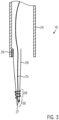
- the test needle has a connection end 22 and a measuring end 23. In the area of the connection end 22, the free spring arm 17 is connected to the test needle 19.
- the test needle 19 is connected to the base spring arm 16 in such a way that in the non-deflected state of the spring arms 16, 17, i.e. when the base spring arm 16 rests on the base plate 13, the test needle 19 is arranged perpendicular to the plane of the base plate 13.
- This test probe 12 and the corresponding test finger 2 are designed such that, when mounted on the test finger 2, the test needle in the non-deflected state is arranged perpendicular to the test area or to a circuit board 4 located in the test area.
- the test needle 19 protrudes a little from the base plate 13 on the test probe 12.
- the test needle 19 has a metal tube which is electrically conductive and has an outer diameter of preferably a maximum of 0.2 mm and in particular a maximum of 0.18 mm.
- a cable 25 is guided in the metal tube 24, which has an electrical conductor which is surrounded by an insulating layer.
- the cable 25 is connected to a conductor track formed on the base plate 13, which is electrically connected to a capacitive measuring device (not shown).
- the conductor of the cable 25 is connected to a capacitive measuring body 26.
- the capacitive measuring body is a metallic ring body which is arranged around the tube and is electrically insulated from it.
- the capacitive measuring body 26 can be a metal ring provided with an insulating layer which is electrically connected to the conductor of the cable 25.
- the capacitive measuring body 26 can also be formed from one or more windings of the cable 25.
- the metal tube 24 serves to shield the cable 25, so that only the capacitive measuring body 26 can enter into a capacitive coupling with a nearby electrical conductor and only its capacitive coupling to this further electrical conductor can be sensed by means of the cable 25.
- a measuring tip 27 is formed at the measuring end 23 of the test needle 19. This measuring tip is only used for mechanical contact with another body.
- the measuring tip can be made of a non-electrically conductive material or provided with an insulating layer. In the present embodiment, it is not used for electrical contact with a contact point on a circuit board.
- the measuring tip can also be designed to be electrically conductive, so that it can be used to establish an electrical connection with a contact point on the circuit board. If such an electrically conductive contact tip is electrically connected to the capacitive measuring body 26, then the contact tip can be taken into account in a capacitive coupling that the capacitive measuring body 26 forms with an electrically conductive object to be measured.
- One embodiment of the measuring tip 27 is formed from a cannula tube 28, which is electrically and mechanically connected at one end to the tube or shield 24 by means of a soldered connection 29.
- the cannula tube has a diameter of, for example, 0.3 mm in the area of the soldered connection 29.
- the cannula tube is formed axially in the direction of the measuring tip 27 and has a diameter of 0.2 mm or less in the area of the measuring tip 27.
- the cannula tube 28 is cut at an angle in the area of the measuring tip, so that an obliquely running outlet opening 30 is produced.
- the cable 25 is guided through the tube 24 and the cannula tube 28 and exits the cannula tube 28 at the outlet opening 30.
- the cable is wound around the cannula tube 28 with, for example, three windings and forms the capacitive measuring body 26.
- the measuring tip 27 itself is electrically conductive and is electrically connected to the tube 24.
- Such an electrically conductive measuring tip has the advantage that the test needle 19 can, for example, come into contact with a calibration surface which has electrically conductive and non-electrically conductive surface sections, so that the position of the test needle 19 and thus the position of a test finger 2 in which the test needle 19 is attached can be calibrated.
- test needle 19 shown is easy to manufacture and has a very small measuring body 26 so that the spatial resolution is correspondingly precise.
- the signal induced on the capacitive measuring body 26 is picked up by the cable 25 from the capacitive measuring body 26 and forwarded to the measuring device. Based on the amplitude of the signal measured in this way, the capacitance formed between the capacitive measuring body 26 and the electrical conductor arranged adjacent to it can be determined. can be determined. At the same time, the location of the capacitive measuring body 26 is recorded, which is predetermined by the location of the test probe 12, which is set by moving the corresponding test finger 2 and is known on the finger tester 1. By simultaneously recording the location and the capacitance when moving the capacitive measuring body 26 in the blind hole, the capacitance that the capacitive measuring body 26 forms with its surroundings can be determined depending on the location. This creates a profile of the capacitance, from which the coating of the inner surface of the blind hole with an electrical conductor can be derived.
- the finger tester 1 has several test fingers 2, each of which is provided with a test probe 12 according to the invention.
- This allows several blind holes or through holes to be measured simultaneously.
- measurement signals are used that differ in their frequency. This can then prevent crosstalk from one measurement to another measurement using appropriate bandpass filters.
- At least one test finger 2 with a test probe 3 with a conventional test needle 10 for electrically contacting a contact point of the circuit board and a further test finger 2 with a test probe 12 according to the invention are provided on each guide rail 6. It can also be expedient to provide two test fingers 2 with conventional test probes 3 and a further test finger 2 with a test probe 12 according to the invention on a guide rail 6.
- the invention can also be applied to a conventional finger tester which has several separate crossbeams which are not arranged on a common crossbeam unit 5.
- a finger tester it is again expedient to provide at least one test finger 2 with a test probe 12 according to the invention and one or more test fingers with conventional test probes 3 per crossbeam.
- the geometry of a blind hole or through hole can be determined very easily and precisely and, on the other hand, the coating with an electrical conductor of the inner surface of the blind hole or through hole can be determined.
- test probe 12 according to the invention can be used in conventional finger testers (flying probe testers). No further mechanical modifications are necessary.
- the finger tester only needs to be provided with a suitable control program that processes the measurement signals generated by the test probe 12 according to the invention. and can apply suitable measuring signals and can control the movement of a test finger 2 with the test probe 12 according to the invention.
- the through-hole 31 is an electrically conductive coating on the inner surface of the hole.
- the hole is then re-drilled a second time a little deeper so that the coating of the hole 37 is removed again in a predetermined section. Errors can arise here if the re-drilling is either not deep enough or too deep so that the edge of the coating in the hole is slightly offset from its desired position.
- the second hole can also be made slightly offset from the first hole if the two holes are not concentric. This leaves a thin, unwanted stripe of the coating in the area of the hole.
- the stripe extends in a direction approximately parallel to the center axis of the hole. Such a stripe can also arise if the second hole is made at a slight angle with respect to the first hole.
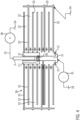
- the circuit board 38 has several layers 32, between which conductor tracks 33 are formed. There are larger and smaller conductor tracks. As a rule, the so-called ground conductor track is the largest conductor track on a circuit board and can often extend over several layers 32. In the measurement method explained below, the ground conductor track is connected to the electrical earth 34 ( Fig. 4 ). Instead of the individual ground conductor tracks, several individual smaller conductor tracks can also be used, which are simultaneously connected to the electrical ground 34.
- the term "ground conductor track” is used to describe one or more conductor tracks which can be simultaneously connected to electrical ground and branch over a larger area of the circuit board 38, in particular over several layers. This connection to the electrical ground 34 is preferably made by placing a movable contact finger of the finger tester on the conductor track, this contact finger having an electrically conductive contact tip which is connected to the electrical ground.
- the capacitive measuring body 26 When the test probe 3 is inserted into the bore, the capacitive measuring body 26 forms an electrical capacitance with the surrounding electrical conductors.
- the aim of this method is to measure this capacitance or its change when the capacitive measuring body is inserted into the bore.
- a signal generator 35 is used to apply a vibration signal to the electrical ground at the via 31.
- This measuring signal flows along the via 31, via a capacitance C1 between the through-hole 31 and the capacitive measuring body 26 into the capacitive measuring body 26 and from there via the cable 25 to an ammeter 36, with which the voltage and thus the capacitance C1 or its change in capacitance when the capacitive measuring body 26 comes close to the through-hole 31 are measured.
- a parasitic capacitance C2 forms between the through-hole 31 and the neighboring conductor tracks. This is particularly relevant when it forms between the through-hole and the ground conductor track. If the ground conductor track were not grounded, the measurement signal would be transmitted to other conductor tracks via the parasitic capacitance via their capacitive coupling (capacitance C3) to the ground conductor track. As a result, the capacitive measuring body would be able to see the measurement signal via further capacitive couplings (capacitance C4) between the capacitive measuring body 26 and the conductor tracks arranged outside the through-hole ( Fig. 5 ). This makes it impossible to determine exactly whether one is measuring the electrical capacitance C1 between the measuring body 26 and the via 31 or the capacitance C4 between the measuring body 26 and one of the other conductor tracks.
- the capacitor C1 represents the coupling between the via 31 and the measuring body 26.
- the capacitor C2 is located between the via 31 and the ground conductor track in the sense of the above description.
- the capacitor C3 is the coupling between the ground conductor track and the other conductor tracks.
- the capacitor C4 represents the coupling of the conductor tracks with the measuring body 26.
- the coupling of the conductor tracks with the measuring body 26 can be made directly through the ground conductor track or through other conductor tracks coupled to the ground conductor track via the capacitor C3. If the coupling is made directly between the ground conductor track and the measuring body 26, then the capacitor C3 is omitted, which is why it is short-circuited with a dashed line in the equivalent circuit diagram and does not need to be taken into account in further consideration.
- connection 34 of the ground conductor to the electrical earth is provided with a switch in the equivalent circuit diagram ( Fig. 6 ), whereby according to the measuring arrangement according to Figure 4 the switch is closed and according to the measuring arrangement Fig. 5 the switch is open.
- the capacitors C2(, C3), C4 are connected in parallel to the capacitor C1. If the series connection of C2(, C3), C4 is larger than C1, then the total capacitance between the via 31 and the measuring body 26 is determined primarily by the series connection of the capacitors C2(, C3), C4 and the current measured by the current measuring device 36 is determined primarily by the series connection of C2(, C3), C4.
- the current measuring device 36 is a current-voltage converter which has an operational amplifier 39 and a measuring resistor 40.
- the operational amplifier is, for example, of the type AD549.
- U m At the output of the current measuring device 36 there is a voltage signal U m which is proportional to the current flowing at the input of the current measuring device.
- One input of the operational amplifier is connected to the measuring body 26 and the other input to the electrical ground.
- both inputs of the operational amplifier 39 are kept at the potential of the electrical ground.
- the capacitors C3 and C4 are therefore arranged between two points, each of which is at the potential of the electrical earth, so that no current flows through them. They are therefore not visible in the measurement.
- the voltage signal from the signal generator 35 is present on one side of the capacitor C2 and the other side of the capacitor C2 is connected to the electrical ground, so that a current flows through this capacitor. This current is not measured by the measuring device because it flows directly to the electrical ground. This current influences the power delivered by the signal generator 35, but not the voltage delivered by the signal generator 35. Since the voltage signal U present on the capacitor C1 and the If the current I flowing through the capacitor is known, the capacitance of the capacitor C1 can be determined from this without the measurement being influenced by the other capacitances C2, C3, C4 if the ground conductor is connected to the electrical earth.
- the capacitive coupling C1 between the measuring body 26 and the via 31 can be measured precisely, whereby the amount of the capacitive coupling C1 can be determined and allows a statement to be made about the geometric size of a defect in the via.
- This method is so precise that it can also be modified so that the signal from the signal generator can be applied to a single conductor track that extends to the through-hole, so that the capacitive coupling of the measuring body to this conductor track can be detected using this signal. This makes it possible to determine the position of the measuring body in the through-hole or to determine that this conductor track correctly conducts the measurement signal to the area of the through-hole.
- the location of the test probe is calibrated relative to the location of the circuit board to be tested by bringing the test probe 12 with its contact tip into contact with the surface of the circuit board.
- This mechanical calibration can be replaced by an electrical calibration, whereby in the electrical calibration a vibration signal is applied to a conductor track adjacent to the through-hole, which is then detected by the test probe or its measuring body.
- This method can also be modified so that several measurement signals with different frequencies are applied to different conductor tracks and/or the through-hole.
- the different frequencies are differentiated during the measurement. This can be done, for example, by connecting a tunable band-pass filter upstream of the current measuring device 36, which can be switched to a frequency band that includes a frequency of one of the signals. This allows several conductor tracks to be detected in the area of a through-hole, provided they are not shielded by a through-hole.
Landscapes
- Physics & Mathematics (AREA)
- General Physics & Mathematics (AREA)
- Engineering & Computer Science (AREA)
- General Engineering & Computer Science (AREA)
- Computer Hardware Design (AREA)
- Microelectronics & Electronic Packaging (AREA)
- Geometry (AREA)
- Environmental & Geological Engineering (AREA)
- Measuring Leads Or Probes (AREA)
- Testing Of Short-Circuits, Discontinuities, Leakage, Or Incorrect Line Connections (AREA)
- Tests Of Electronic Circuits (AREA)
Applications Claiming Priority (4)
| Application Number | Priority Date | Filing Date | Title |
|---|---|---|---|
| DE102018101031.1A DE102018101031A1 (de) | 2018-01-18 | 2018-01-18 | Prüfnadel, Prüfsonde und Fingertester zum Testen von Leiterplatten |
| DE102018125666 | 2018-10-16 | ||
| EP19701082.0A EP3740767A1 (fr) | 2018-01-18 | 2019-01-17 | Aiguille de test capacitif pour mesurer des couches électriquement conductrices dans des trous de carte de circuit imprimé |
| PCT/EP2019/051148 WO2019141777A1 (fr) | 2018-01-18 | 2019-01-17 | Aiguille de test capacitif pour mesurer des couches électriquement conductrices dans des trous de carte de circuit imprimé |
Related Parent Applications (1)
| Application Number | Title | Priority Date | Filing Date |
|---|---|---|---|
| EP19701082.0A Division EP3740767A1 (fr) | 2018-01-18 | 2019-01-17 | Aiguille de test capacitif pour mesurer des couches électriquement conductrices dans des trous de carte de circuit imprimé |
Publications (2)
| Publication Number | Publication Date |
|---|---|
| EP4471435A2 true EP4471435A2 (fr) | 2024-12-04 |
| EP4471435A3 EP4471435A3 (fr) | 2025-03-05 |
Family
ID=65041754
Family Applications (2)
| Application Number | Title | Priority Date | Filing Date |
|---|---|---|---|
| EP19701082.0A Pending EP3740767A1 (fr) | 2018-01-18 | 2019-01-17 | Aiguille de test capacitif pour mesurer des couches électriquement conductrices dans des trous de carte de circuit imprimé |
| EP24199871.5A Pending EP4471435A3 (fr) | 2018-01-18 | 2019-01-17 | Aiguille de test, sonde de test et testeur à doigt pour tester les circuits imprimés |
Family Applications Before (1)
| Application Number | Title | Priority Date | Filing Date |
|---|---|---|---|
| EP19701082.0A Pending EP3740767A1 (fr) | 2018-01-18 | 2019-01-17 | Aiguille de test capacitif pour mesurer des couches électriquement conductrices dans des trous de carte de circuit imprimé |
Country Status (7)
| Country | Link |
|---|---|
| US (2) | US11774495B2 (fr) |
| EP (2) | EP3740767A1 (fr) |
| JP (2) | JP7608162B2 (fr) |
| KR (3) | KR102735009B1 (fr) |
| CN (2) | CN111566488B (fr) |
| TW (1) | TWI697676B (fr) |
| WO (1) | WO2019141777A1 (fr) |
Families Citing this family (10)
| Publication number | Priority date | Publication date | Assignee | Title |
|---|---|---|---|---|
| CN112305405A (zh) * | 2020-10-12 | 2021-02-02 | 景旺电子科技(珠海)有限公司 | 线路板四线测试系统及测试方法 |
| EP4019889B1 (fr) * | 2020-12-28 | 2024-05-01 | Mitutoyo Corporation | Configuration de détection de position inductive pour indiquer la position d'un stylet de dispositif de mesure |
| TWI775274B (zh) | 2021-01-14 | 2022-08-21 | 欣興電子股份有限公司 | 電路板內介電層厚度之量測裝置及量測方法 |
| TWI736500B (zh) | 2021-01-14 | 2021-08-11 | 欣興電子股份有限公司 | 電磁式量測電路板的介電層厚度的量測探針設備及方法 |
| TWI774191B (zh) | 2021-01-14 | 2022-08-11 | 欣興電子股份有限公司 | 電路板內介電層厚度之量測裝置及量測方法 |
| CN113030580B (zh) * | 2021-03-05 | 2023-01-10 | 健鼎(无锡)电子有限公司 | 一种电测方法 |
| CN113866587B (zh) * | 2021-08-20 | 2024-05-24 | 苏州国科测试科技有限公司 | 一种飞针测试设备 |
| KR102741114B1 (ko) * | 2023-06-19 | 2024-12-10 | 주식회사 에스엠전자 | 정전용량 및 상대적 누설분포 분석 알고리즘 기반 수배전반 실시간 감전 안전진단 시스템 |
| WO2025178269A1 (fr) * | 2024-02-20 | 2025-08-28 | 엘지이노텍 주식회사 | Dispositif d'inspection de circuit |
| DE102024121234A1 (de) * | 2024-07-25 | 2026-01-29 | Atg Luther & Maelzer Gmbh | Verfahren und Vorrichtung zum Bestimmen einer Stublänge |
Citations (6)
| Publication number | Priority date | Publication date | Assignee | Title |
|---|---|---|---|---|
| WO2003048787A1 (fr) | 2001-12-07 | 2003-06-12 | Atg Test Systems Gmbh & Co. Kg | Sonde d'essai pour testeur a pattes, et testeur a pattes correspondant |
| US8431834B2 (en) | 2009-06-16 | 2013-04-30 | Ciena Corporation | Method for assuring counterbore depth of vias on printed circuit boards and printed circuit boards made accordingly |
| WO2014140029A1 (fr) | 2013-03-13 | 2014-09-18 | Dtg International Gmbh | Système de traverse pour dispositif d'essai de circuits imprimés ainsi que dispositif d'essai équipé de ce système |
| US20150047892A1 (en) | 2013-08-15 | 2015-02-19 | Huawei Technologies Co., Ltd. | Pcb backdrilling method and system |
| US9341670B2 (en) | 2014-05-20 | 2016-05-17 | International Business Machines Corporation | Residual material detection in backdrilled stubs |
| US9459285B2 (en) | 2013-07-10 | 2016-10-04 | Globalfoundries Inc. | Test probe coated with conductive elastomer for testing of backdrilled plated through holes in printed circuit board assembly |
Family Cites Families (30)
| Publication number | Priority date | Publication date | Assignee | Title |
|---|---|---|---|---|
| US3840802A (en) * | 1972-08-10 | 1974-10-08 | Rockwell International Corp | Mutual inductance coupling probe for testing the integrity of through-hole plating in printed circuit boards |
| SU563616A1 (ru) * | 1975-02-11 | 1977-06-30 | Московский Ордена Ленина Энергетический Институт | Токовихревой преобразователь |
| US4072895A (en) * | 1976-01-27 | 1978-02-07 | Rogachev Viktor Igorevich | Eddy current converter for non-destructive testing of electrically conducting coating in holes of printed circuit boards |
| US5274336A (en) | 1992-01-14 | 1993-12-28 | Hewlett-Packard Company | Capacitively-coupled test probe |
| JPH0816683B2 (ja) * | 1992-07-28 | 1996-02-21 | 株式会社日本マイクロニクス | プローブ針の製造方法 |
| DE69836486T2 (de) * | 1997-07-30 | 2007-10-11 | Candescent Technologies Corp., San Jose | Magnetischer stromdetektor und kurzschlusserkennung in einer plattenstruktur |
| JP2000028642A (ja) | 1998-07-13 | 2000-01-28 | Mitsubishi Materials Corp | コンタクトプローブ |
| US6744268B2 (en) | 1998-08-27 | 2004-06-01 | The Micromanipulator Company, Inc. | High resolution analytical probe station |
| JP2001208775A (ja) | 2000-01-27 | 2001-08-03 | Mitsubishi Materials Corp | コンタクトプローブ及びその製造方法 |
| AU2001272733A1 (en) | 2000-07-19 | 2002-02-05 | Orbotech Ltd. | Apparatus and method for electrical testing of electrical circuits |
| JP2003185695A (ja) | 2001-12-20 | 2003-07-03 | Seiko Epson Corp | 配線パターン検査方法および配線パターン検査装置 |
| DE10220343B4 (de) * | 2002-05-07 | 2007-04-05 | Atg Test Systems Gmbh & Co. Kg Reicholzheim | Vorrichtung und Verfahren zum Prüfen von Leiterplatten und Prüfsonde |
| DE10320925B4 (de) | 2003-05-09 | 2007-07-05 | Atg Test Systems Gmbh & Co.Kg | Verfahren zum Testen von unbestückten Leiterplatten |
| US6933730B2 (en) * | 2003-10-09 | 2005-08-23 | Agilent Technologies, Inc. | Methods and apparatus for testing continuity of electrical paths through connectors of circuit assemblies |
| KR101098635B1 (ko) * | 2004-02-13 | 2011-12-23 | 큐알쥐 리미티드 | 정전용량 센서 |
| JP4954492B2 (ja) | 2005-04-18 | 2012-06-13 | 東京エレクトロン株式会社 | プローブおよびその製造方法 |
| US7669321B1 (en) | 2005-07-13 | 2010-03-02 | Cisco Technology, Inc. | Methods for verifying correct counter-bore depth and precision on printed circuit boards |
| US7268571B1 (en) | 2006-03-20 | 2007-09-11 | Texas Instruments Incorporated | Method for validating and monitoring automatic test equipment contactor |
| JP2007278820A (ja) * | 2006-04-06 | 2007-10-25 | Murata Mfg Co Ltd | 電界プローブ及び電界測定システム |
| JP4494396B2 (ja) | 2006-12-25 | 2010-06-30 | 日本航空電子工業株式会社 | 接続部材 |
| GB0718677D0 (en) * | 2007-09-25 | 2007-10-31 | 3M Innovative Properties Co | Capacitive sensor and proximity detector using it |
| KR101154519B1 (ko) | 2010-05-27 | 2012-06-13 | 하이콘 주식회사 | 스프링 콘택트 구조 |
| JP2012021804A (ja) | 2010-07-12 | 2012-02-02 | Taiyo Kogyo Co Ltd | フライング検査用接触子の保持構造及び回路基板のフライング検査装置 |
| CN102043121A (zh) | 2010-07-21 | 2011-05-04 | 北大方正集团有限公司 | 电路板背钻孔的检测方法及检测电路板背钻孔的测试设备 |
| CN102788888B (zh) | 2012-07-27 | 2014-12-10 | 中国科学院电工研究所 | 扫描探针显微镜进针装置及方法 |
| ITMI20122023A1 (it) | 2012-11-28 | 2014-05-29 | Technoprobe Spa | Sonda di contatto a sbalzo [cantilever] per una testa di misura |
| CN205103284U (zh) | 2015-11-10 | 2016-03-23 | 昆山璁慧物资有限公司 | 可调式弹性飞针测试针 |
| KR102560535B1 (ko) * | 2016-07-01 | 2023-07-28 | 주식회사 로보터스 | 정전 용량형 센서 |
| FR3069639B1 (fr) * | 2017-07-26 | 2019-08-30 | Pfeiffer Vacuum | Sonde de reniflage, detecteur de fuites et procede de detection de fuites |
| KR102636487B1 (ko) * | 2018-10-26 | 2024-02-14 | 삼성전자주식회사 | 신호 전송기 및 이를 구비하는 반도체 소자 검사 장치 |
-
2019
- 2019-01-17 EP EP19701082.0A patent/EP3740767A1/fr active Pending
- 2019-01-17 EP EP24199871.5A patent/EP4471435A3/fr active Pending
- 2019-01-17 US US16/960,434 patent/US11774495B2/en active Active
- 2019-01-17 CN CN201980007361.XA patent/CN111566488B/zh active Active
- 2019-01-17 JP JP2020540268A patent/JP7608162B2/ja active Active
- 2019-01-17 CN CN202410899071.3A patent/CN118858712A/zh active Pending
- 2019-01-17 KR KR1020207023032A patent/KR102735009B1/ko active Active
- 2019-01-17 KR KR1020247031668A patent/KR102859343B1/ko active Active
- 2019-01-17 KR KR1020257030005A patent/KR20250136939A/ko active Pending
- 2019-01-17 WO PCT/EP2019/051148 patent/WO2019141777A1/fr not_active Ceased
- 2019-01-18 TW TW108101944A patent/TWI697676B/zh active
-
2023
- 2023-08-24 US US18/454,906 patent/US20230400509A1/en active Pending
-
2024
- 2024-10-23 JP JP2024186554A patent/JP2025013932A/ja active Pending
Patent Citations (8)
| Publication number | Priority date | Publication date | Assignee | Title |
|---|---|---|---|---|
| WO2003048787A1 (fr) | 2001-12-07 | 2003-06-12 | Atg Test Systems Gmbh & Co. Kg | Sonde d'essai pour testeur a pattes, et testeur a pattes correspondant |
| US8431834B2 (en) | 2009-06-16 | 2013-04-30 | Ciena Corporation | Method for assuring counterbore depth of vias on printed circuit boards and printed circuit boards made accordingly |
| WO2014140029A1 (fr) | 2013-03-13 | 2014-09-18 | Dtg International Gmbh | Système de traverse pour dispositif d'essai de circuits imprimés ainsi que dispositif d'essai équipé de ce système |
| US9459285B2 (en) | 2013-07-10 | 2016-10-04 | Globalfoundries Inc. | Test probe coated with conductive elastomer for testing of backdrilled plated through holes in printed circuit board assembly |
| US20150047892A1 (en) | 2013-08-15 | 2015-02-19 | Huawei Technologies Co., Ltd. | Pcb backdrilling method and system |
| US9341670B2 (en) | 2014-05-20 | 2016-05-17 | International Business Machines Corporation | Residual material detection in backdrilled stubs |
| US9488690B2 (en) | 2014-05-20 | 2016-11-08 | International Business Machines Corporation | Residual material detection in backdrilled stubs |
| US9739825B2 (en) | 2014-05-20 | 2017-08-22 | International Business Machines Corporation | Residual material detection in backdrilled stubs |
Also Published As
| Publication number | Publication date |
|---|---|
| TW201932849A (zh) | 2019-08-16 |
| KR102859343B1 (ko) | 2025-09-12 |
| CN118858712A (zh) | 2024-10-29 |
| US20230400509A1 (en) | 2023-12-14 |
| KR102735009B1 (ko) | 2024-11-28 |
| JP2025013932A (ja) | 2025-01-28 |
| EP3740767A1 (fr) | 2020-11-25 |
| US11774495B2 (en) | 2023-10-03 |
| TWI697676B (zh) | 2020-07-01 |
| KR20200110667A (ko) | 2020-09-24 |
| JP2021510828A (ja) | 2021-04-30 |
| CN111566488B (zh) | 2024-07-19 |
| JP7608162B2 (ja) | 2025-01-06 |
| WO2019141777A1 (fr) | 2019-07-25 |
| KR20240145063A (ko) | 2024-10-04 |
| EP4471435A3 (fr) | 2025-03-05 |
| KR20250136939A (ko) | 2025-09-16 |
| CN111566488A (zh) | 2020-08-21 |
| US20200348359A1 (en) | 2020-11-05 |
Similar Documents
| Publication | Publication Date | Title |
|---|---|---|
| WO2019141777A1 (fr) | Aiguille de test capacitif pour mesurer des couches électriquement conductrices dans des trous de carte de circuit imprimé | |
| DE2659976C2 (de) | Vorrichtung zur Herstellung einer elektrischen Verbindung zwischen einem in einer dynamischen elektrischen Prüfung befindlichen Bauteil und einer Prüfeinrichtung | |
| EP3126851B1 (fr) | Intercalaire de contact, dispositif de test électrique et procédé de fabrication d'un intercalaire de contact | |
| EP0853242B1 (fr) | Procédé pour tester des cartes de circuits imprimés | |
| DE10002099A1 (de) | Sonde mit verteilten Widerständen und Verfahren | |
| EP1186898B1 (fr) | Procédé et appareil pour tester des circuits imprimés | |
| EP2754086A1 (fr) | Procédé de test d'une bobine d'antenne | |
| EP3788388B1 (fr) | Dispositif capteur et procédé de détermination d'une tension alternative | |
| DE102016107970A1 (de) | Koppelelement für ein kapazitives Füllstandsmessgerät | |
| DE10333101B4 (de) | Kalibrierungseinrichtung für die Kalibrierung eines Testerkanals einer Testereinrichtung, Testersystem und Verfahren zum Kalibrieren eines Testerkanals | |
| EP0772054B1 (fr) | Procédé et appareil pour tester des structures de conducteur | |
| EP1982198B1 (fr) | Système de contrôle pour porte-circuit | |
| EP1920263B1 (fr) | Procede pour tester des cartes de circuits imprimes de grandes surfaces non equipees, au moyen d'un testeur a pattes | |
| DE102018101031A1 (de) | Prüfnadel, Prüfsonde und Fingertester zum Testen von Leiterplatten | |
| EP2347272B1 (fr) | Détermination des propriétés d'un dispositif électrique | |
| EP3265834B1 (fr) | Dispositif de contact électrique | |
| EP2125280B1 (fr) | Dispositif pour usiner des pièces | |
| DE102020122065B4 (de) | Kontaktanordnung mit einer Messvorrichtung zum Erfassen eines Kontaktierungszustands der Kontaktanordnung mittels eines akustischen Signals | |
| DE102024110653B3 (de) | Messsystem und Verfahren zur Charakterisierung einer mehrschichtigen Struktur mit schichtweise unterschiedlichen ohmschen Eigenschaften, Sensormodul für ein Messsystem, Fertigungsanlage für eine mehrschichtige Struktur mit schichtweise unterschiedlichen ohmschen Eigenschaften | |
| DE102024121234A1 (de) | Verfahren und Vorrichtung zum Bestimmen einer Stublänge | |
| EP3444575B1 (fr) | Dispositif capteur destiné à la mesure potentiometrique d'une hauteur de niveau de remplissage dans un recipient | |
| DE102018222660A1 (de) | Verfahren zum Erkennen von Defekten oder Längenänderungen an nadelförmigen Messobjekt, Vorrichtung zur Anwendung des Verfahrens und Leiterplatte als Bestandteil der Vorrichtung | |
| DE3703030A1 (de) | Testanordnung fuer hochgeschwindigkeits-ic | |
| EP3312624A1 (fr) | Système et procédé de test de vibration pour cartes de circuits imprimés | |
| DE102015221839A1 (de) | Messsystem und Verfahren |
Legal Events
| Date | Code | Title | Description |
|---|---|---|---|
| PUAI | Public reference made under article 153(3) epc to a published international application that has entered the european phase |
Free format text: ORIGINAL CODE: 0009012 |
|
| STAA | Information on the status of an ep patent application or granted ep patent |
Free format text: STATUS: THE APPLICATION HAS BEEN PUBLISHED |
|
| AC | Divisional application: reference to earlier application |
Ref document number: 3740767 Country of ref document: EP Kind code of ref document: P |
|
| AK | Designated contracting states |
Kind code of ref document: A2 Designated state(s): AL AT BE BG CH CY CZ DE DK EE ES FI FR GB GR HR HU IE IS IT LI LT LU LV MC MK MT NL NO PL PT RO RS SE SI SK SM TR |
|
| REG | Reference to a national code |
Ref country code: DE Ref legal event code: R079 Free format text: PREVIOUS MAIN CLASS: G01R0001067000 Ipc: G01R0001070000 |
|
| PUAL | Search report despatched |
Free format text: ORIGINAL CODE: 0009013 |
|
| AK | Designated contracting states |
Kind code of ref document: A3 Designated state(s): AL AT BE BG CH CY CZ DE DK EE ES FI FR GB GR HR HU IE IS IT LI LT LU LV MC MK MT NL NO PL PT RO RS SE SI SK SM TR |
|
| RIC1 | Information provided on ipc code assigned before grant |
Ipc: G01R 1/067 20060101ALI20250124BHEP Ipc: G01R 31/28 20060101ALI20250124BHEP Ipc: G01R 1/073 20060101ALI20250124BHEP Ipc: G01R 1/07 20060101AFI20250124BHEP |
|
| RAP3 | Party data changed (applicant data changed or rights of an application transferred) |
Owner name: ATG LUTHER & MAELZER GMBH |
|
| STAA | Information on the status of an ep patent application or granted ep patent |
Free format text: STATUS: REQUEST FOR EXAMINATION WAS MADE |
|
| 17P | Request for examination filed |
Effective date: 20250826 |