EP4474808A1 - Kapazitive mikroelektrodenvorrichtung zur erfassung einer biologischen aktivität in einer probe und verfahren zur verwendung solch einer mikroelektrodenvorrichtung - Google Patents
Kapazitive mikroelektrodenvorrichtung zur erfassung einer biologischen aktivität in einer probe und verfahren zur verwendung solch einer mikroelektrodenvorrichtung Download PDFInfo
- Publication number
- EP4474808A1 EP4474808A1 EP23178096.6A EP23178096A EP4474808A1 EP 4474808 A1 EP4474808 A1 EP 4474808A1 EP 23178096 A EP23178096 A EP 23178096A EP 4474808 A1 EP4474808 A1 EP 4474808A1
- Authority
- EP
- European Patent Office
- Prior art keywords
- sample
- electrode assembly
- electrodes
- sensing
- activity
- Prior art date
- Legal status (The legal status is an assumption and is not a legal conclusion. Google has not performed a legal analysis and makes no representation as to the accuracy of the status listed.)
- Withdrawn
Links
Images


Classifications
-
- G—PHYSICS
- G01—MEASURING; TESTING
- G01N—INVESTIGATING OR ANALYSING MATERIALS BY DETERMINING THEIR CHEMICAL OR PHYSICAL PROPERTIES
- G01N33/00—Investigating or analysing materials by specific methods not covered by groups G01N1/00 - G01N31/00
- G01N33/48—Biological material, e.g. blood, urine; Haemocytometers
- G01N33/50—Chemical analysis of biological material, e.g. blood, urine; Testing involving biospecific ligand binding methods; Immunological testing
- G01N33/5005—Chemical analysis of biological material, e.g. blood, urine; Testing involving biospecific ligand binding methods; Immunological testing involving human or animal cells
-
- G—PHYSICS
- G01—MEASURING; TESTING
- G01N—INVESTIGATING OR ANALYSING MATERIALS BY DETERMINING THEIR CHEMICAL OR PHYSICAL PROPERTIES
- G01N33/00—Investigating or analysing materials by specific methods not covered by groups G01N1/00 - G01N31/00
- G01N33/48—Biological material, e.g. blood, urine; Haemocytometers
- G01N33/483—Physical analysis of biological material
- G01N33/4833—Physical analysis of biological material of solid biological material, e.g. tissue samples, cell cultures
- G01N33/4836—Physical analysis of biological material of solid biological material, e.g. tissue samples, cell cultures using multielectrode arrays
-
- G—PHYSICS
- G01—MEASURING; TESTING
- G01N—INVESTIGATING OR ANALYSING MATERIALS BY DETERMINING THEIR CHEMICAL OR PHYSICAL PROPERTIES
- G01N33/00—Investigating or analysing materials by specific methods not covered by groups G01N1/00 - G01N31/00
- G01N33/48—Biological material, e.g. blood, urine; Haemocytometers
- G01N33/483—Physical analysis of biological material
- G01N33/487—Physical analysis of biological material of liquid biological material
- G01N33/48707—Physical analysis of biological material of liquid biological material by electrical means
- G01N33/48735—Investigating suspensions of cells, e.g. measuring microbe concentration
-
- G—PHYSICS
- G01—MEASURING; TESTING
- G01N—INVESTIGATING OR ANALYSING MATERIALS BY DETERMINING THEIR CHEMICAL OR PHYSICAL PROPERTIES
- G01N33/00—Investigating or analysing materials by specific methods not covered by groups G01N1/00 - G01N31/00
- G01N33/48—Biological material, e.g. blood, urine; Haemocytometers
- G01N33/50—Chemical analysis of biological material, e.g. blood, urine; Testing involving biospecific ligand binding methods; Immunological testing
- G01N33/53—Immunoassay; Biospecific binding assay; Materials therefor
- G01N33/543—Immunoassay; Biospecific binding assay; Materials therefor with an insoluble carrier for immobilising immunochemicals
- G01N33/54366—Apparatus specially adapted for solid-phase testing
- G01N33/54373—Apparatus specially adapted for solid-phase testing involving physiochemical end-point determination, e.g. wave-guides, FETS, gratings
- G01N33/5438—Electrodes
Definitions
- the present invention relates to a microelectrode device for sensing a biological activity within a sample and a method of using such a microelectrode device.
- Bio activity can relate to electrical activity from neurons firing action potentials.
- Biological activity can relate to chemical activity from neurotransmitters being released.
- Microelectrode arrays enable the simultaneous recording of the electrical activity of neurons via multiple electrodes.
- Complementary metal-oxide semiconductor (CMOS) MEA systems can have integrated >10,000 on-chip electrodes using metal pads with a pitch of ⁇ 10 ⁇ m using active pixel sensors (APS) or switchmatrix (SM) or sub-array multiplexing (SAM) [1-4].
- APS active pixel sensors
- SM switchmatrix
- SAM sub-array multiplexing
- CMOS MEA Complementary metal-oxide semiconductor
- APS active pixel sensors
- SM switchmatrix
- SAM sub-array multiplexing
- neurons must be cultured on top of CMOS MEAs, making it difficult to accommodate various experimental setups such as transparent or stretchable electrodes.
- the materials of the chip can also corrode during long-term exposure to liquids, incurring extra packaging complexity to protect the chip and to prevent the cells from being damaged by the materials released by the chip [6].
- Aptamers are single-stranded oligonucleotides that are designed in vitro to bind specific analytes of interest. There are aptamers that undergo large conformational rearrangements of negatively charged phosphodiester backbones in the presence of specific analytes. Aptamers can have a high selectivity, as the structure switching only occurs in the presence of the specific analyte for which they have been designed (contrary to conventional bioreceptors such as antibodies that have challenges of cross-reactivity and promiscuity).
- An aspect of the invention relates to a microelectrode device for sensing a biological activity within a sample.
- the microelectrode device comprises an electrode assembly with electrodes for contacting the sample, and an electronic equipment which is connected to the electrodes of the electrode assembly.
- the electronic equipment is configured to evaluate one or more capacitances between the electrodes for sensing the biological activity within the sample.
- the microelectrode device enables that the one or more capacitances include one or more electrical double layer capacitances of one or more electrical double layers which are formed when the electrodes are brought into contact with the sample. Evaluating a capacitance between two electrodes can relate to measuring the capacitance, i.e. the mutual capacitance.
- Evaluating capacitances between electrodes can relate to detecting a change in a capacitance.
- the electrode assembly can be configured for contacting the sample and the electronic equipment can be configured to apply a bias, an AC (alternate current) potential, a current, etc. to the sample such that the electrical double layer capacitance can be modulated.
- AC alternate current
- a current etc.
- the biological activity relates to an electrical activity within the sample
- the electronic equipment is configured to evaluate the one or more capacitances for sensing the electrical activity.
- the electrical activity can relate to an electrochemical activity of ions being transported from the outside of a biological cell, such as a neuron, into the inside and/or from ions being transported from the inside of a biological cell, such as a neuron, into the outside.
- the electronic equipment can be configured to evaluate frequencies in a range of 100-5000 Hz or similar, which are typical for electrical activities.
- the biological activity relates to a chemical activity within the sample
- the electrode assembly is functionalized, in particular with aptamers i(a), for modifying the electrical double layer capacitance depending on the chemical activity
- the electronic equipment is configured to evaluate the one or more capacitances for sensing the chemical activity.
- Aptamers can be designed to chemically bind to target molecules, such as neurotransmitters like serotonin or dopamine, wherein the aptamers undergo a conformational change, such as regards length, shape, charge distribution, etc., when binding to the target molecules, thereby modifying the electrical double layer and the electrical double layer capacitance.
- electrical activity and chemical activity can be sensed at the same time.
- the electronic equipment can be configured to evaluate frequencies of 1 Hz, 0.1 Hz or similar, which are typical for chemical activities.
- the electrode assembly includes electrodes which are arranged in a form of an array.
- the array can be designed to sense an area of the sample, such as a rectangular or quadratic area, such as an area of 500 micrometer x 500 micrometer, 1 millimeter x 1 millimeter, etc.
- the electrode assembly includes electrodes which form a cross-coupled capacitive microelectrode array, and the electronic equipment is configured to apply a code division multiplexing method for evaluating the one or more capacitances.
- a compact, flexibly configurable electrode assembly is enabled, while interconnects between the electrode assembly and the electronic equipment are minimized.
- a methodology can be applied for creating an electrical double layer capacitance on a CMOS chip.
- the electrode assembly does not have to be an external cross-coupled array, it can be any metal electrode or metal electrodes on-chip or off-chip.
- a capacitance is applied to analog or digital conversion circuits to measure the electrical double layer capacitance for sensing a biological activity such as action potential or neural activity.
- a capacitance to an analog or digital conversion circuit can convert an electrical double layer capacitance of an array of electrical double layer capacitances to an analog voltage, an analog current, an analog impedance and to digital values.
- the electronic equipment is configured to enable sensing of the biological activity with a frequency of 2 kHz or more.
- the microelectrode device enables sensing biological activity in the form of an electrical activity and of a chemical activity.
- the electrode assembly is configured to enable sensing of the biological activity with a pitch of 50 micrometers or less.
- the microelectrode device enables sensing biological activity with a high spatial resolution.
- the electrode assembly has a transparent configuration, in particular enabling the use of standard microscopy equipment.
- the invention further relates to a method of using a microelectrode device as described.
- the method comprises: providing the microelectrode device, providing a sample, bringing the sample in contact with the electrodes of the electrode assembly, and enabling forming within the sample of one or more electrical double layers having one or more electrical double layer capacitances at one or more surfaces of the electrode, operating the electronic equipment to evaluate the one or more capacitances for sensing the biological activity.
- the biological activity relates to an electrical activity
- the electronic equipment is operated for sensing the electrical activity
- the biological activity relates to a chemical activity
- the method further comprises functionalizing the electrode assembly, in particular with aptamers, for modifying the electrical double layer capacitance depending on the chemical activity, and the electronic equipment is operated for sensing the chemical activity.
- functionalizing the electrode assembly includes one or more of: an in-flow functionalization, an outside functionalization, a hybrid functionalization, and a microfluidics functionalization.
- the sample includes one or more of electrogenic cells, chemogenic cells and cells that have ion channel activities.
- the sample includes one or more of neurons, glia, muscle cells, and cardiomyocites.
- the sample is provided in-vitro or in-vivo.
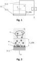
- Fig. 1 schematically shows a microelectrode device 1 according to an embodiment of the present invention for sensing a biological activity within a sample S.
- the sample S can relate to in-vitro or in-vivo tissue with neurons.
- the biological activity is a physiological activity, e.g. signaling, metabolism, etc.
- the microelectrode device 1 comprises an electrode assembly 11 and electronic equipment 12.
- the electrode assembly includes electrodes 11.1, 11.2 which are configured for contacting the sample S.
- the electrode assembly 11 includes a first and a second electrode 11.1, 11.2.
- the electronic equipment 12 is connected to the electrodes 11.1, 11.2 of the electrode assembly 11, for example via electrically conductive wires.
- the electronic equipment 12 is configured to evaluate a capacitance C between the electrodes 11.1, 11.2 for sensing the biological activity within the sample.
- the microelectrode device 1 enables that the capacitance C includes an electrical double layer capacitance C_EDL of an electrical double layer which is formed when the electrodes 11.1, 11.2 are brought into contact with the sample S.
- the electrical double layer having electrical double layer capacitance C_EDL is formed at a surface of the first electrode 11.1.
- sensing a biological activity can relate to a single electrical double layer capacitance.
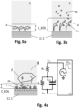
- Fig. 2 schematically shows an embodiment of a sample S which is in contact with the first electrode 11.1.
- the sample S includes ions i, molecules m and a neuron n.
- the sample S relates to an in-vitro or in-vivo sample of tissue with neurons.
- the first electrode 11.1 is negatively charged, which effects that positively charged ions are accumulated on the surface of the first electrode 11.1. This results in the formation of an electrical double layer having an electrical double layer capacitance C_EDL.
- C_EDL electrical double layer capacitance
- an electrical activity occurs because of the electrochemical activity of ions i which are transported from the outside of the neuron n to the inside and/or from the inside of the neuron n to the outside.
- This transfer of ions i also effects a change in the ion concentration within the electrical double layer, which results in a change of the electrical double layer capacitance C_EDL.
- detecting a change in the capacitance C between the electrodes 11.1, 11.2, which includes the electrical double layer capacitance C_EDL sensing a biological activity in the form of an electrical activity is enabled.
- Fig. 3a, 3b schematically show a sample S which is in contact with the first electrode 11.1.
- the surface of the first electrode 11.1 is functionalized with aptamers a, wherein an electrical double layer having electrical double layer capacitance C_EDL is formed.
- the aptamers a are designed to chemically bind to target molecules m, for example to neurotransmitters such as serotonin or dopamine.
- neurotransmitters such as serotonin or dopamine.
- the aptamers a undergo a conformational change (length, shape, charge distribution, etc.) when binding to the target molecules m, such as serotonin or dopamine released by neurons, thereby modifying the electrical double layer, such as its length, ion concentration, etc., and the electrical double layer capacitance C_EDL.
- a conformational change length, shape, charge distribution, etc.
- the electrical double layer such as its length, ion concentration, etc.
- electrical activities have a frequency range of, for example, between 100 Hz - 5 kHz, while chemical activities have a frequency of for example below 1 Hz, such as 0.1 Hz. Accordingly, by spectral separation, electrical activities within the sample S can be separated from chemical activities.
- chemical activities can relate to an accumulation of small, fast chemical events, wherein the accumulation results in a change of the electrical double layer capacitance in a frequency range of below 1 Hz, such as 0.1 Hz.
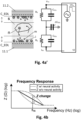
- Fig. 4a schematically shows a microelectrode device 1 according to an embodiment of the present invention.
- the electrode assembly includes an electrode 11.1 which is configured for contacting a sample S.
- the electronic equipment 12 is connected to the sample S and includes a signal generator for transmitting a transmit signal V_TX to the sample S.
- the electronic equipment 12 is connected to the electrode 11.1 for receiving a receive signal I_RX (in the form of a current signal) from the electrode 11.1, which can be converted into a voltage signal V_TX within the electronic equipment 12 .
- Fig. 4a illustrates the equivalent circuit between the transmit signal V_TX and the receive signal I_RX when the sample S is brought into contact with the electrode 11.1.
- the equivalent circuit includes a fluid resistor R_S which is in serial connection with an electric double layer capacitor C_EDL, which is in parallel connection with an electrode resistor R_E.
- the surface charge of the electrode 11.1 in solution is balanced by oppositely charged counter ions accumulating at the surface, forming an electric double layer having electric double layer capacitance C_EDL.
- the counter ions in solution reside at the surface, separated by a distance on the order of 1nm for physiological conditions, resulting in a large capacitance on the order of for example ⁇ 170 pF for 100 square micrometers.
- the neuron can depolarize during an action potential, wherein the electrochemical potential of the ions on the surface changes, causing a corresponding change in the electric double layer capacitance C_EDL.
- Fig. 4a' schematically shows a microelectrode device 1 according to an embodiment of the present invention. Contrary to Fig. 4a , in Fig. 4a' a first and a second electrode 11.1, 11.2 are shown. In the equivalent circuit, each electrode corresponds to an electrode resistor R_E connected in parallel with an electric double layer capacitor C_EDL, wherein between them, a delta electrical double layer capacitance ⁇ C_EDL is connected to ground, which corresponds to a change of the electrical double layer capacitance because of an electrical and/or a chemical activity within the sample S.
- Fig. 4b schematically shows the frequency response of the impedance Z with neural activity and without neural activity of the embodiment of the microelectrode device 1 according to Fig. 4a .
- Fig. 5a schematically shows a microelectrode device 1 according to an embodiment of the present invention.
- the electrode assembly includes a first and second sensing electrode 11.1, 11.2, and a first and second reference electrode 11.1', 11.2'.
- the first and second sensing electrodes 11.1, 11.2 are functionalized with an aptamer a designed for molecules m, such as a neurotransmitter.
- the first and second reference electrodes 11.1', 11.2' are functionalized with a scrambled aptamer a' which is designed to not interact with the molecules m.
- the scrambled aptamer a' has the same chemical signature as the aptamer a (charge, mass, functional groups).
- the sensing electrodes 11.1, 11.2 and the reference electrodes 11.1', 11.2' are connected to the electronic equipment 12.
- the electronic equipment 12 is configured to evaluate the capacitance between the sensing electrodes 11.1, 11.2 and the capacitance between the reference electrodes 11.1', 11.2'.
- the capacitance between the reference electrodes 11.1', 11.2' is C' and does not change due to the presence of the molecules m.
- the capacitance between the sensing electrodes 11.1, 11.2 is C and changes upon the presence of the molecules m.
- the electronic equipment 12 can be configured to subtract the capacitance C' between the reference electrodes 11.1', 11.2' from the capacitance C between the sensing electrodes 11.1, 11.2 in order to improve sensor selectivity.
- Fig. 5b shows an electrode assembly 11 according to the embodiment of the microelectrode device 1 shown in Fig. 5a .
- Fig. 6 schematically shows a microelectrode device 1 according to an embodiment of the present invention.
- the microelectrode device 1 includes an electrode assembly 11 and an electronic equipment 12.
- the electrode assembly 11 includes electrodes 11.r, 11.c which form a cross-coupled capacitive microelectrode array.
- a substrate 11.s such as a silicon substrate or similar having length L and width W supports a set of column electrodes 11.c which can have, e.g., the form of rectangular cuboids.
- the column electrodes 11.c In direction of the width W of the substrate 11.s, the column electrodes 11.c are separated from each other.
- the column electrodes 11.c have length L.
- a similar set of row electrodes 11.r is arranged in orthogonal direction above the column electrodes 11.c and separated from the column electrodes 11.c by an isolator (not shown in Fig. 6 ).
- the electrodes 11.r, 11.c are configured for contacting a sample S.
- an array of capacitances C0, C1, ... includes an electrical double layer capacitance C_EDL when the electrodes 11.r, 11.c are brought into contact with the sample S.
- the microelectrode device 1 includes an electronic equipment 12 which is configured for transmission of transmit signals V_TX0, V_TX1, ... to the row electrodes 11.r, and for reception of receive signals V_RX0, V_RX1, ... from the column electrodes 11.c in order to evaluate each capacitance of the array of capacitances C0, C1, ....
- Fig. 7 schematically shows a signal processing method which enables evaluating each capacitance of the array of electrodes C0, C1, ... shown in Fig. 6 .
- the electronic equipment is configured to apply a 2-D code division multiplexing.
- Each electrode of the row electrodes is driven by a synchronous and orthogonal set of transmit signals V_TX0, V_TX1, ... of orthogonal codes, such as pseudo-random Walsh codes.
- the capacitance C0, C1, ... between each column and row, which each include a respective electrical double layer capacitance C_EDL, represents the ion concentration of the corresponding coordinate.
- Each receive signal V_RX0, V_RX1, ... represents a weighted sum of capacitances C0, C1, ...
- an electronic equipment 12 for a N-channel microelectrode device 1 requires only 2 ⁇ N interconnects and ⁇ N readout circuits, relaxing integration complexity and improving area efficiency while measuring all channels concurrently.
- Fig. 6, 7 illustrate four row electrodes 11.r and four column electrodes 11.c (4x4 electrodes), and a 2-D code division multiplexing.
- the invention is not limited to a particular number of electrodes.
- the electrode assembly 11 can include 16x16 electrodes, 32x32 electrodes, etc.
- an microelectrode device 1 with an electrode assembly 11 having 32x32 electrodes achieves 1,024 independent recording channels.
- the invention is not limited to square arrays.
- the number of row electrodes 11.r does not have to be as the number of column electrodes 11.c.
- the electronic equipment (12) can include clock generators, bias circuits for controlling transmit circuits for transmission of transmit signals V_TX0, V_TX1, and for controlling readout circuits for reception of receive signals V_RX0, V_RX1, ....
- the transmit circuits can include controller circuits, weighting circuits, and similar for generating the transmit signals V_TX0, V_TX1, ....
- the readout circuits can include switching circuits serially connected to an amplifier chain, a decoder and a multiplexer.
- the amplifier chain can include low noise amplifiers (LNA), variable gain amplifiers (VGA), an analog buffer, and similar.
- the decoder can include multiplier circuits, switch capacitor integrators, and similar.
- Fig. 8a shows an embodiment of an electrode assembly 11, which has a set of 32 row electrodes 11.r, and a set of 32 column electrodes.
- Fig. 8b shows a SEM image of a cutout of the electrode assembly 11.
- Fig. 8c schematically shows a 3-dimensional structure of a cutout of the electrode assembly 11 illustrated in Figs. 8a, 8b with electrodes 11.r, 11.c.
- Fig. 8c' schematically shows a 3-dimenstional structure of a cutout of the electrode assembly 11 illustrated in Figs. 8a, 8b with electrodes 11.r, 11.c for sensing an electrical activity of a neuron n.
- Fig. 8a shows an embodiment of an electrode assembly 11, which has a set of 32 row electrodes 11.r, and a set of 32 column electrodes.
- Fig. 8b shows a SEM image of a cutout of the electrode assembly 11.
- Fig. 8c schematically shows a 3-dimensional structure of a cutout of the electrode assembly 11
- FIG. 8c schematically shows a 3-dimenstional structure of a cutout of the electrode assembly 11 illustrated in Figs. 8a, 8b with electrodes 11.r, 11.c which are functionalized with aptamers a for sensing a chemical activity of molecules m.
- Fig. 9a shows a fluorescent image of an electrode assembly 11 having arranged a sample S with neurons.
- Fig. 9b shows for a particular location of the electrode assembly 11 the result of the electronic equipment 12 evaluating the capacitance at that location, wherein evaluation relates to determining a change of the capacitance.
- Fig. 10 shows a sequence of four activity maps of an electrode assembly 11 having arranged a sample S with neurons.
- the activity maps are generated by the electronic equipment 12 by evaluating the capacitances, wherein evaluation relates to determining a change of the capacitances.
- Figs. 11a, 11b, 11c show the activity for activity map #3 at adjacent locations.
- Fig. 11b shows an activity at its location of the sample S, wherein Figs. 11a, 11c do not show an activity at their locations the sample S.
- a distance between the electrode assembly 11 and the electronic equipment 12 can be 10 cm or more.
- the electrode assembly 11 can have a transparent, soft or stretchable configuration such as based on PDMS (polydimethylsiloxane), hydrogels or similar.
- PDMS polydimethylsiloxane
- the electrode assembly 11 can have a an corrode resistive configuration and can enable long-term exposure to liquids
- the electrodes 11.1, 11.2; 11.r, 11.c of the electrode assembly 11 can include gold (Au), a conductive polymer such as PDOT:PSS (poly(3,4-ethylenedioxythiophene) polystyrene sulfonate), transparent conductors such as ITO (indium tin oxide), or similar.
- the electrodes 11.1, 11.2; 11.r, 11.c of the electrode assembly 11 can be supported by a glass plate, a silicon substrate, or similar.
- the electrodes 11.r, 11.c of the electrode assembly 11 can be fabricated by depositing two layers of gold (e.g. 150nm thickness) separated by a layer of SiN (silicon nitride) or another dielectric material such as PDMS, hydrogels, other nonconductive polymers or similar (e.g. 200nm thickness).
- the electronic equipment 12 can be partially or fully fabricated in CMOS (Complementary Metal-Oxide-Semiconductor) or similar.
- CMOS Complementary Metal-Oxide-Semiconductor
- Fig. 12 shows schematically possible method steps of a method of using a microelectrode device 1 according to the present invention.
- a microelectrode device 1 according to the present invention is provided.
- a sample S is provided.
- the sample S is brought in contact with the electrodes and forming within the sample S of an electrical double layer having an electrical double layer capacitance E_EDL at a surface of an electrode 11 is enabled.
- the electronic equipment 12 is operated to evaluate a capacitance C for sensing the biological activity.
- the method can further comprise a step of functionalizing the electrode assembly 11 for modifying the electrical double layer capacitance C_EDL depending on a chemical activity.
- the electrode assembly 11 can be functionalized with aptamers a.
- Functionalizing the electrodes with aptamers can include a preparation of aptamers.
- In-Flow functionalization can be applied.
- the presence of a flow cell opens the possibility of a functionalization operated directly with the electronic equipment 12.
- aptamers can be pushed with e.g. a syringe on the sensing area, allowing real-time monitoring of the changes in capacitance during functionalization, and an analysis of how much of this change is retained when rinsing with a buffer solution.
- An incubation time can be e.g. two hours.
- Static functionalization can be applied.
- PDMS walls can be arranged to cleanly separate sides of the electrode assembly, so that solutions do not affect each other.
- Aptamer solutions can be applied with pipettes.
- An incubation time can be e.g. two hours. Different aptamer solutions can be applied.
- Hybrid functionalization can be applied. First, an static functionalization can be applied, wherein a first set of aptamer solutions is used. Thereafter, within the setup, a further aptamer solution is applied for functionalizing remaining electrodes.
- Functionalization of embodiments of a microelectrode array illustrated in Figs. 6 , 8a, 8b, 8c can relate to pattern aptamers in the region where rows and columns overlap (cf. Fig. 8c" ). Differential functionalization either between individual Rx, Tx, or electrodes is possible.
Landscapes
- Health & Medical Sciences (AREA)
- Life Sciences & Earth Sciences (AREA)
- Engineering & Computer Science (AREA)
- Biomedical Technology (AREA)
- Immunology (AREA)
- Chemical & Material Sciences (AREA)
- Physics & Mathematics (AREA)
- Urology & Nephrology (AREA)
- Hematology (AREA)
- Molecular Biology (AREA)
- General Physics & Mathematics (AREA)
- General Health & Medical Sciences (AREA)
- Food Science & Technology (AREA)
- Medicinal Chemistry (AREA)
- Pathology (AREA)
- Analytical Chemistry (AREA)
- Biochemistry (AREA)
- Cell Biology (AREA)
- Biotechnology (AREA)
- Microbiology (AREA)
- Biophysics (AREA)
- Optics & Photonics (AREA)
- Tropical Medicine & Parasitology (AREA)
- Investigating Or Analyzing Materials By The Use Of Electric Means (AREA)
Priority Applications (2)
| Application Number | Priority Date | Filing Date | Title |
|---|---|---|---|
| EP23178096.6A EP4474808A1 (de) | 2023-06-07 | 2023-06-07 | Kapazitive mikroelektrodenvorrichtung zur erfassung einer biologischen aktivität in einer probe und verfahren zur verwendung solch einer mikroelektrodenvorrichtung |
| PCT/EP2024/065682 WO2024251922A1 (en) | 2023-06-07 | 2024-06-06 | A microelectrode device for sensing a biological activity within a sample and a method of using such a microelectrode device |
Applications Claiming Priority (1)
| Application Number | Priority Date | Filing Date | Title |
|---|---|---|---|
| EP23178096.6A EP4474808A1 (de) | 2023-06-07 | 2023-06-07 | Kapazitive mikroelektrodenvorrichtung zur erfassung einer biologischen aktivität in einer probe und verfahren zur verwendung solch einer mikroelektrodenvorrichtung |
Publications (1)
| Publication Number | Publication Date |
|---|---|
| EP4474808A1 true EP4474808A1 (de) | 2024-12-11 |
Family
ID=86732670
Family Applications (1)
| Application Number | Title | Priority Date | Filing Date |
|---|---|---|---|
| EP23178096.6A Withdrawn EP4474808A1 (de) | 2023-06-07 | 2023-06-07 | Kapazitive mikroelektrodenvorrichtung zur erfassung einer biologischen aktivität in einer probe und verfahren zur verwendung solch einer mikroelektrodenvorrichtung |
Country Status (2)
| Country | Link |
|---|---|
| EP (1) | EP4474808A1 (de) |
| WO (1) | WO2024251922A1 (de) |
Citations (2)
| Publication number | Priority date | Publication date | Assignee | Title |
|---|---|---|---|---|
| US20050227373A1 (en) * | 2002-06-24 | 2005-10-13 | Denis Flandre | Method and device for high sensitivity detection of the presence of dna and other probes |
| US20100221846A1 (en) * | 2007-10-12 | 2010-09-02 | Nxp B.V. | Sensor, a sensor array, and a method of operating a sensor |
-
2023
- 2023-06-07 EP EP23178096.6A patent/EP4474808A1/de not_active Withdrawn
-
2024
- 2024-06-06 WO PCT/EP2024/065682 patent/WO2024251922A1/en not_active Ceased
Patent Citations (2)
| Publication number | Priority date | Publication date | Assignee | Title |
|---|---|---|---|---|
| US20050227373A1 (en) * | 2002-06-24 | 2005-10-13 | Denis Flandre | Method and device for high sensitivity detection of the presence of dna and other probes |
| US20100221846A1 (en) * | 2007-10-12 | 2010-09-02 | Nxp B.V. | Sensor, a sensor array, and a method of operating a sensor |
Non-Patent Citations (5)
| Title |
|---|
| CHOI WOOJUN ET AL: "A 1,024-Channel, 64-Interconnect, Capacitive Neural Interface Using a Cross-Coupled Microelectrode Array and 2-Dimensional Code-Division Multiplexing", 2023 IEEE SYMPOSIUM ON VLSI TECHNOLOGY AND CIRCUITS (VLSI TECHNOLOGY AND CIRCUITS), JSAP, 11 June 2023 (2023-06-11), pages 1 - 2, XP034383173, DOI: 10.23919/VLSITECHNOLOGYANDCIR57934.2023.10185425 * |
| HU KANGPING ET AL: "A Large-Scale Multimodal CMOS Biosensor Array With 131,072 Pixels and Code-Division Multiplexed Readout", IEEE SOLID-STATE CIRCUITS LETTERS, IEEE, vol. 4, 3 February 2021 (2021-02-03), pages 48 - 51, XP011840637, DOI: 10.1109/LSSC.2021.3056515 * |
| HU KANGPING ET AL: "High Frequency Dielectric Spectroscopy Array with Code Division Multiplexing for Biological Imaging", 2019 IEEE BIOMEDICAL CIRCUITS AND SYSTEMS CONFERENCE (BIOCAS), IEEE, 17 October 2019 (2019-10-17), pages 1 - 4, XP033644732, DOI: 10.1109/BIOCAS.2019.8919173 * |
| LU M S C ET AL: "5x5 CMOS capacitive sensor array for detection of the neurotransmitter dopamine", BIOSENSORS AND BIOELECTRONICS, ELSEVIER SCIENCE LTD, UK, AMSTERDAM , NL, vol. 26, no. 3, 15 November 2010 (2010-11-15), pages 1093 - 1097, XP027393263, ISSN: 0956-5663, [retrieved on 20100919] * |
| ZHANG JIAN ET AL: "An interdigitated microelectrode based aptasensor for real-time and ultratrace detection of four organophosphorus pesticides", BIOSENSORS AND BIOELECTRONICS, ELSEVIER SCIENCE LTD, UK, AMSTERDAM , NL, vol. 150, 15 November 2019 (2019-11-15), XP086018665, ISSN: 0956-5663, [retrieved on 20191115], DOI: 10.1016/J.BIOS.2019.111879 * |
Also Published As
| Publication number | Publication date |
|---|---|
| WO2024251922A1 (en) | 2024-12-12 |
Similar Documents
| Publication | Publication Date | Title |
|---|---|---|
| EP2201368B1 (de) | Sensor, sensor-array sowie verfahren zu deren betrieb | |
| US8702921B2 (en) | Biosensors array and method for operating a biosensor array | |
| EP3254096B1 (de) | Organisches transistorbasiertes system für elektrophysiologische überwachung von zellen und verfahren zur überwachung der zellen | |
| EP3045902A1 (de) | Sensor mit Elektrolyt-Gate zum Speziesnachweis | |
| US6503701B1 (en) | Analytic sensor apparatus and method | |
| KR20190034139A (ko) | 전기화학 감지, 정전용량 감지 및 전계 방출 감지를 위한 나노구조 어레이 기반의 센서들 | |
| US8097134B2 (en) | Addressable chem/bio chip array | |
| US11850586B2 (en) | Analyte sensor package and method for analyzing fluid samples | |
| EP4474808A1 (de) | Kapazitive mikroelektrodenvorrichtung zur erfassung einer biologischen aktivität in einer probe und verfahren zur verwendung solch einer mikroelektrodenvorrichtung | |
| WO2017003126A1 (ko) | 바이오 센서 및 바이오 센서 어레이 | |
| Choi et al. | A 1,024-Channel, 64-Interconnect, capacitive neural interface using a cross-coupled microelectrode array and 2-dimensional code-division multiplexing | |
| WO2010027785A2 (en) | Measurement of biological targets | |
| US20250067705A1 (en) | Electrochemical measurement apparatuses and methods for monitoring and controlling ph | |
| CN109668949B (zh) | 具有分配化学品和微流体盖件的分析物传感器封装体 | |
| US12270777B2 (en) | 2D microfluidic structure | |
| KR101441964B1 (ko) | 센서 시스템 | |
| Yusof et al. | On-chip microelectrode capacitance measurement for biosensing applications | |
| Lin et al. | CMOS bioelectronics: Current and future trends | |
| JP2023133145A (ja) | バイオセンサチップ | |
| CN110207737B (zh) | 线阵列结构的微带天线传感器系统、传感器、检测及制备方法 | |
| KR20220066061A (ko) | 다중 감지 기능을 갖는 다중 픽셀 가스 마이크로센서 제조공정 | |
| CN118032901B (zh) | 离子敏感场效应晶体管与延展式场效应生物检测芯片 | |
| Ravindran et al. | Biochemical sensing with an arrayed silicon nanowire platform | |
| Lam et al. | Development of highly sensitive interdigitated electrodes (IDEs) with APTES/GOx based lab-on-chip biosensor to determine glucose level | |
| US20240282696A1 (en) | BioFET sensing chip |
Legal Events
| Date | Code | Title | Description |
|---|---|---|---|
| PUAI | Public reference made under article 153(3) epc to a published international application that has entered the european phase |
Free format text: ORIGINAL CODE: 0009012 |
|
| STAA | Information on the status of an ep patent application or granted ep patent |
Free format text: STATUS: THE APPLICATION HAS BEEN PUBLISHED |
|
| AK | Designated contracting states |
Kind code of ref document: A1 Designated state(s): AL AT BE BG CH CY CZ DE DK EE ES FI FR GB GR HR HU IE IS IT LI LT LU LV MC ME MK MT NL NO PL PT RO RS SE SI SK SM TR |
|
| STAA | Information on the status of an ep patent application or granted ep patent |
Free format text: STATUS: THE APPLICATION IS DEEMED TO BE WITHDRAWN |
|
| 18D | Application deemed to be withdrawn |
Effective date: 20250612 |