EP4474904A2 - Reflektierender fotomaskenrohling mit einer ein- oder zweilagigen hartmaske und verfahren zur herstellung einer reflektierenden fotomaske durch trockenätzen des reflektierenden fotomaskenrohlings - Google Patents
Reflektierender fotomaskenrohling mit einer ein- oder zweilagigen hartmaske und verfahren zur herstellung einer reflektierenden fotomaske durch trockenätzen des reflektierenden fotomaskenrohlings Download PDFInfo
- Publication number
- EP4474904A2 EP4474904A2 EP24178169.9A EP24178169A EP4474904A2 EP 4474904 A2 EP4474904 A2 EP 4474904A2 EP 24178169 A EP24178169 A EP 24178169A EP 4474904 A2 EP4474904 A2 EP 4474904A2
- Authority
- EP
- European Patent Office
- Prior art keywords
- layer
- film
- hard mask
- pattern
- dry etching
- Prior art date
- Legal status (The legal status is an assumption and is not a legal conclusion. Google has not performed a legal analysis and makes no representation as to the accuracy of the status listed.)
- Pending
Links
Images


Classifications
-
- G—PHYSICS
- G03—PHOTOGRAPHY; CINEMATOGRAPHY; ANALOGOUS TECHNIQUES USING WAVES OTHER THAN OPTICAL WAVES; ELECTROGRAPHY; HOLOGRAPHY
- G03F—PHOTOMECHANICAL PRODUCTION OF TEXTURED OR PATTERNED SURFACES, e.g. FOR PRINTING, FOR PROCESSING OF SEMICONDUCTOR DEVICES; MATERIALS THEREFOR; ORIGINALS THEREFOR; APPARATUS SPECIALLY ADAPTED THEREFOR
- G03F1/00—Originals for photomechanical production of textured or patterned surfaces, e.g., masks, photo-masks, reticles; Mask blanks or pellicles therefor; Containers specially adapted therefor; Preparation thereof
- G03F1/22—Masks or mask blanks for imaging by radiation of 100nm or shorter wavelength, e.g. X-ray masks, extreme ultraviolet [EUV] masks; Preparation thereof
- G03F1/24—Reflection masks; Preparation thereof
-
- G—PHYSICS
- G03—PHOTOGRAPHY; CINEMATOGRAPHY; ANALOGOUS TECHNIQUES USING WAVES OTHER THAN OPTICAL WAVES; ELECTROGRAPHY; HOLOGRAPHY
- G03F—PHOTOMECHANICAL PRODUCTION OF TEXTURED OR PATTERNED SURFACES, e.g. FOR PRINTING, FOR PROCESSING OF SEMICONDUCTOR DEVICES; MATERIALS THEREFOR; ORIGINALS THEREFOR; APPARATUS SPECIALLY ADAPTED THEREFOR
- G03F1/00—Originals for photomechanical production of textured or patterned surfaces, e.g., masks, photo-masks, reticles; Mask blanks or pellicles therefor; Containers specially adapted therefor; Preparation thereof
- G03F1/38—Masks having auxiliary features, e.g. special coatings or marks for alignment or testing; Preparation thereof
- G03F1/48—Protective coatings
-
- G—PHYSICS
- G03—PHOTOGRAPHY; CINEMATOGRAPHY; ANALOGOUS TECHNIQUES USING WAVES OTHER THAN OPTICAL WAVES; ELECTROGRAPHY; HOLOGRAPHY
- G03F—PHOTOMECHANICAL PRODUCTION OF TEXTURED OR PATTERNED SURFACES, e.g. FOR PRINTING, FOR PROCESSING OF SEMICONDUCTOR DEVICES; MATERIALS THEREFOR; ORIGINALS THEREFOR; APPARATUS SPECIALLY ADAPTED THEREFOR
- G03F1/00—Originals for photomechanical production of textured or patterned surfaces, e.g., masks, photo-masks, reticles; Mask blanks or pellicles therefor; Containers specially adapted therefor; Preparation thereof
- G03F1/54—Absorbers, e.g. of opaque materials
- G03F1/58—Absorbers, e.g. of opaque materials having two or more different absorber layers, e.g. stacked multilayer absorbers
-
- G—PHYSICS
- G03—PHOTOGRAPHY; CINEMATOGRAPHY; ANALOGOUS TECHNIQUES USING WAVES OTHER THAN OPTICAL WAVES; ELECTROGRAPHY; HOLOGRAPHY
- G03F—PHOTOMECHANICAL PRODUCTION OF TEXTURED OR PATTERNED SURFACES, e.g. FOR PRINTING, FOR PROCESSING OF SEMICONDUCTOR DEVICES; MATERIALS THEREFOR; ORIGINALS THEREFOR; APPARATUS SPECIALLY ADAPTED THEREFOR
- G03F1/00—Originals for photomechanical production of textured or patterned surfaces, e.g., masks, photo-masks, reticles; Mask blanks or pellicles therefor; Containers specially adapted therefor; Preparation thereof
- G03F1/68—Preparation processes not covered by groups G03F1/20 - G03F1/50
- G03F1/80—Etching
Definitions
- the present invention relates to a method for manufacturing a reflective photomask used for manufacturing a semiconductor device or the like, and a reflective photomask blank used for manufacturing the same as a material of the reflective photomask.
- phase shift mask has been developed as a method for improving resolution of a transfer pattern.
- phase shift method The principle of a phase shift method is that a phase of transmitted light that has passed through an opening of a phase shift film of a photomask is adjusted to be inverted by about 180 degrees with respect to the phase of the transmitted light that has passed through a part of the phase shift film adjacent to the opening, such that the transmitted light interferes at a boundary part between the opening and the part adjacent to the opening to decrease the light intensity, and as a result, the resolution and focal depth of the transfer pattern are improved, and the photomask using this principle is generally called a phase shift mask.
- phase shift mask blank as a material of a phase shift mask used for manufacturing a phase shift mask has a structure in which a phase shift film is laminated on a transparent substrate such as a glass substrate and a film formed of a material containing chromium (Cr) is laminated on the phase shift film.
- the phase shift film usually has a phase difference of 175 to 185 degrees and a transmittance of about 6 to 30% with respect to exposure light, and is mainly a film containing silicon (Si), and particularly a film formed of a material containing molybdenum (Mo) and silicon (Si).
- a film formed of a material containing chromium is adjusted to have a thickness that provides a desired optical density together with the phase shift film, and the film formed of a material containing chromium is generally used as a light shielding film and a hard mask layer when the phase shift film is etched.
- a method for manufacturing a phase shift mask by patterning a phase shift film from a phase shift mask blank in which a phase shift film formed of a material containing silicon and a light shielding film formed of a material containing chromium are formed in this order on a transparent substrate specifically, the following method is common. First, a resist film is formed on a light shielding film that is formed of a material containing chromium of a phase shift mask blank, and a pattern is drawn and developed on the resist film with light or an electron beam to form a resist pattern. Next, using the resist pattern as an etching mask, the light shielding film formed of a material containing chromium is etched using chlorine-based gas to form a pattern of the light shielding film.
- a phase shift film formed of a material containing silicon is etched using fluorine-based gas to form a pattern of the phase shift film, and then the resist pattern is removed, and the pattern of the light shielding film is etched and removed using chlorine-based gas.
- the light shielding film is left outside a part where the pattern (circuit pattern) of the phase shift film is formed, and an outer peripheral edge of the phase shift mask is set as a light shielding part (light shielding pattern) having a total optical density of the phase shift film and the light shielding film of 3 or more. This is to prevent the exposure light from leaking from the outer peripheral edge of the phase shift mask and irradiating the resist film on an adjacent chip of a wafer with the exposure light from a part located outside the circuit pattern when the circuit pattern is transferred to the wafer using a wafer exposure apparatus.
- a method for forming such a light shielding pattern As a method for forming such a light shielding pattern, a method of forming a pattern of a phase shift film, removing a resist pattern, forming a new resist film, forming a resist pattern in which a resist film is left on an outer peripheral edge of a phase shift mask by pattern writing and development, and etching a film formed of a material containing chromium using the resist pattern as an etching mask to leave a light shielding film on the outer peripheral edge of the phase shift mask is generally used.
- dry etching using gas plasma is mainly used for etching.
- Dry etching using chlorine-based gas (chlorine-based dry etching) is used for dry etching of a film formed of a material containing chromium
- dry etching using fluorine-based gas (fluorine-based dry etching) is used for dry etching of a film containing silicon or a film containing molybdenum and silicon.
- a technique for finely forming a circuit pattern of a phase shift mask is also required.
- an assist pattern of a line pattern that assists resolution of a main pattern of the phase shift mask needs to be formed smaller than the main pattern so as not to be transferred to the wafer when the circuit pattern is transferred to the wafer using the wafer exposure apparatus.
- a line width of the assist pattern of the line pattern of the circuit on the phase shift mask is required to be about 40 nm.
- a chemically amplified resist capable of forming a fine pattern contains a base resin, an acid generator, a surfactant, and the like, and since a lot of reactions in which an acid generated by exposure acts as a catalyst can be applied, high sensitivity can be achieved, and a mask pattern such as a pattern of a fine phase shift film having a line width of 0.1 um or less can be formed by using the chemically amplified resist.
- the resist is applied onto the photomask blank by spin coating with a resist coater.
- a thickness of the resist film used for the phase shift mask blank of the tip end product is 100 to 150 nm.
- the reason why it is difficult to form a finer assist pattern in the phase shift mask is that since an aspect ratio of the resist pattern for forming the assist pattern formed on the light shielding film formed of a material containing chromium is high, the resist pattern falls down due to an impact by a developer or an impact by pure water during a rinsing process in the development process of forming the resist pattern.
- the resist film is thinned.
- the resist film when the resist film disappears during dry etching of the light shielding film formed of the material containing chromium, pinhole defects are formed in the light shielding film formed of the material containing chromium, and when the phase shift film is dry-etched using the light shielding film formed of the material containing chromium as an etching mask, plasma during etching of the phase shift film reaches the phase shift film through the pinholes, and pinhole defects are also formed in the phase shift film, such that a normal phase shift mask cannot be manufactured.
- a hard mask layer formed of a material containing silicon but no chromium is further provided on the light shielding film formed of a material containing chromium.
- the hard mask layer formed of the material containing silicon but no chromium is a thin film having a thickness of 5 to 15 nm, and a thickness of the resist layer formed on the hard mask layer is as thin as 80 to 110 nm.
- the light shielding film formed of the material containing chromium is dry-etched using chlorine-based gas containing oxygen, it is required to perform 100 to 300% over-etching of clear time in addition to clear time at which the light shielding film formed of the material containing chromium disappears. This is because chlorine-based dry etching containing oxygen is isotropic etching in which a chemical component is dominant, and a pattern of a light shielding film formed of a material containing chromium is insufficiently etched at a boundary part with the phase shift film to form a trail shape, such that a desired pattern width is not stably formed.
- etching is isotropic etching in which a chemical component is dominant, chlorine-based plasma containing oxygen moves in a vertical direction and a horizontal direction with respect to the substrate, and causes side etching in the pattern of the light shielding film formed of the material containing chromium, and in order to make a critical dimension (CD), which is a pattern line width, uniform over the entire surface of the mask, it is required to obtain the same side etching amount over the entire surface of the mask. To this end, long-time dry etching is required until the amount of side etching is stabilized by causing saturation.
- CD critical dimension
- phase shift film formed of the material containing silicon is dry-etched using the fluorine-based gas
- about 20% over-etching (for example, short over-etching for 1 to 6 seconds) of clear time at the maximum is performed in addition to the clear time at which the phase shift film formed of the material containing silicon disappears
- the transparent substrate in contact with the phase shift film is also slightly etched by dry etching to adjust a phase difference to 175 to 185 degrees with respect to exposure light.
- a phase shift film formed of a material containing silicon generally has an initial phase difference set to 175 to 179 degrees, and a desired phase difference, that is, 175 to 185 degrees by digging the transparent substrate by over-etching.
- the over-etching may be performed in a short time in the fluorine-based dry etching.
- the fluorine-based dry etching is anisotropic etching in which a physical component is dominant, the pattern of the phase shift film formed of the material containing silicon does not have a trail shape at the boundary part with the substrate, the fluorine-based plasma moves in the vertical direction with respect to the substrate surface, and the CD of the light shielding film formed of the material containing chromium that functions as an etching mask is faithfully reproduced, and thus, the long-time over-etching is not required.
- a resist film for forming a pattern of a hard mask layer formed of a material containing silicon needs to have a corresponding thickness.
- the hard mask layer formed of the material containing silicon serves as an etching mask when the light shielding film formed of the material containing chromium is dry-etched using the chlorine-based gas, and has sufficient etching resistance to the chlorine-based gas, the hard mask layer formed of the material containing silicon can be thinned.
- the time for fluorine-based dry etching on the hard mask layer is shortened, and as a result, the resist film required to form the pattern of the hard mask layer formed of the material containing silicon can also be thinned.
- a resist film used for etching of the hard mask layer that is, a resist film first used for a phase shift mask blank can be thinned by using a hard mask layer formed of a material containing silicon.
- the aspect ratio of the resist pattern is reduced by thinning the resist film, the influence of a physical impact when applying a developer in the development process of forming the resist pattern or a physical impact when applying pure water in a rinsing process is reduced, an excellent assist pattern can be formed, and high resolution of the transfer pattern can be realized.
- a method for manufacturing a phase shift mask by patterning a phase shift film from a phase shift mask blank in which a phase shift film formed of a material containing silicon, a light shielding film formed of a material containing chromium, and a hard mask layer formed of a material containing silicon are formed in this order on a transparent substrate specifically, the following method is common.
- a resist film is formed on a hard mask layer, and a pattern is drawn and developed on the resist film with light or an electron beam to form a resist pattern.
- a hard mask layer formed of a material containing silicon is dry-etched using fluorine-based gas to form a pattern of the hard mask layer, and then the resist pattern is removed.
- the light shielding film formed of a material containing chromium is dry-etched using chlorine-based gas to form a pattern of the light shielding film. Furthermore, using the pattern of the light shielding film as an etching mask, a phase shift film formed of a material containing silicon is dry-etched using fluorine-based gas to form a pattern of the phase shift film and simultaneously to remove the pattern of the hard mask layer, and then the pattern of the light shielding film is etched and removed using chlorine-based gas.
- the extreme ultraviolet region light is easily absorbed by any substance, and transmission lithography such as photolithography using ArF excimer laser light of the related art cannot be used. Therefore, in the EUV lithography, a reflection optical system is used. Since a wavelength of the extreme ultraviolet region light used in the EUV lithography is 13 to 14 nm and a wavelength of ArF excimer laser light of the related art is 193 nm, the exposure wavelength is short as compared in the photolithography using the ArF excimer laser light of the related art, and it is possible to transfer a finer pattern on the photomask.
- the photomask used in the EUV lithography generally has a structure in which a reflective film that reflects extreme ultraviolet region light, a protective film that protects the reflective film, and a light absorbing film that absorbs the extreme ultraviolet region light are formed in this order on a substrate such as a glass substrate.
- a reflective film a multilayer reflective film, in which a reflectance when the surface of the reflective film is irradiated with the extreme ultraviolet region light is increased by alternately laminating a low refractive index layer and a high refractive index layer, is used.
- a molybdenum (Mo) layer is used as the low refractive index layer of the multilayer reflective film
- a silicon (Si) layer is used as the high refractive index layer.
- a ruthenium (Ru) film is usually used as the protective film.
- a material having a high absorption coefficient for EUV light specifically, for example, a material containing chromium (Cr) or tantalum (Ta) as a main component is used for the light absorbing film.
- a method for manufacturing a reflective photomask by patterning a light absorbing film from a reflective photomask blank in which a reflective film that reflects extreme ultraviolet region light, a protective film that protects the reflective film, and a light absorbing film that absorbs the extreme ultraviolet region light are formed in this order on a substrate specifically, the following method is common. First, a resist film is formed on a light absorbing film, and a pattern is drawn and developed on the resist film with light or an electron beam to form a resist pattern. Next, a pattern of the light absorbing film is formed, and then the resist pattern is removed.
- assist patterns of a line pattern and a space pattern which assist the resolution of the main pattern, are further reduced as the main pattern is miniaturized, and a line width of the assist pattern is required to be reduced to about 30 nm, and particularly about 25 nm. Therefore, as compared with the phase shift mask blank, the reflective photomask blank requires further thinning of the resist film.
- the thickness of the resist film needs to be 80 nm or less.
- an optical system that changes a numerical aperture NA of an exposure machine from 0.33 to 0.55 is used.
- the assist patterns of the line pattern and the space pattern, which assist the resolution of the main pattern are further reduced as the main pattern is miniaturized, and the line width of the assist pattern is required to be reduced to about 25 nm, and particularly about 20 nm. Therefore, in the reflective photomask blank used in the exposure machine with an aperture ratio of 0.55, it is required to make the resist film even thinner. In addition, it is required not only to reduce the thickness of the resist film but also to reduce deterioration of resolution due to disappearance of the fine line pattern during the dry etching process.
- fluorine-based dry etching is anisotropic etching in which a physical component is dominant, and an etching rate with respect to the resist pattern is relatively high. Therefore, when the resist pattern is too thin, the resist pattern disappears during dry etching with respect to the light absorbing film, pinhole defects are formed in the light absorbing film, and thus, a normal reflective photomask cannot be manufactured.
- the resist film In order to prevent the pinhole defects, it is required to make the resist film thick. However, the thicker the resist film, the higher the aspect ratio of the resist pattern to form a finer assist pattern. Therefore, in the development process of forming a resist pattern, the resist pattern falls down due to the impact by the developer or the impact by the pure water during the rinsing process, which makes it impossible to obtain the desired resolution.
- WO 2012/105508 A describes a reflective mask blank for EUV lithography in which a layer that reflects EUV light, an absorbing layer that absorbs EUV light, and a hard mask layer are formed in this order on a substrate.
- the absorbing layer is a layer containing at least one of tantalum (Ta) and palladium (Pd) as a main component
- the hard mask layer is a layer containing chromium (Cr), nitrogen (N) or oxygen (O), and hydrogen (H) and having a total content of Cr, N or Cr, and O of 85 of 99.9 at% and a content of H of 0.1 to 15 at%
- surface roughness of the hard mask layer is small, an etching selection ratio under the etching conditions of the absorbing layer is sufficiently high, a crystalline state becomes amorphous, and the surface roughness can be sufficiently reduced. Therefore, line edge roughness of the pattern of the hard mask layer and the pattern of the absorbing layer formed using the pattern of
- WO 2012/105508 A describes a procedure for forming a pattern on a reflective mask blank for EUV lithography as follows. First, a resist film is formed on a hard mask layer of an EUV mask blank, and a pattern is formed on the resist film using an electron beam lithography machine. Next, using the patterned resist film as a mask, etching is performed by a chlorine-based gas process to form a pattern on the hard mask layer. Next, using the patterned hard mask layer as a mask, etching is performed by a fluorine-based gas process to form a pattern on an absorbing layer. Next, etching is performed by a chlorine-based gas process to remove the hard mask layer.
- the absorbing layer is patterned by fluorine-based dry etching using a CrNH film or a CrOH film as a hard mask layer and a film containing tantalum as an absorbing layer.
- the film (CrNH film or CrOH film) formed of the material containing chromium has high resistance to fluorine-based dry etching and thus has a low etching rate
- the film containing tantalum as a main component has low resistance to fluorine-based dry etching and thus has a high etching rate
- the hard mask layer can be thinned.
- the film containing tantalum is patterned by chlorine-based dry etching, but as the hard mask layer becomes thinner, a reduction amount of the resist film during dry etching also decreases, such that the resist film formed on the hard mask layer can be thinned.
- the aspect ratio of the resist pattern is reduced, and the impact by the developer during the development process of resist pattern formation or the impact by the pure water during the rinsing process is reduced, such that the hard mask layer provides an excellent assist pattern.
- the hard mask layer formed of the material containing chromium is dry-etched using chlorine-based gas containing oxygen, it is required to perform 100 to 300% over-etching of clear time in addition to clear time at which the hard mask layer formed of the material containing chromium disappears, and therefore, in this case, it is not possible to reduce the thickness of the resist film to 80 nm or less.
- a film formed of a material containing chromium has resistance to chlorine-based dry etching containing no oxygen and fluorine-based dry etching, and can be removed by chlorine-based dry etching containing oxygen. Therefore, when a hard mask layer formed of a material containing chromium is peeled off by dry etching using chlorine-based gas containing oxygen after the light absorbing film is patterned, a protective film that protects the multilayer reflective film is exposed to oxygen and chlorine plasma.
- a ruthenium-based material generally used for a protective film has low resistance to chlorine-based dry etching containing oxygen, and may disappear during peeling of the hard mask layer formed of the material containing chromium, and a process window of a dry etching process using chlorine-based gas containing oxygen is narrowed.
- a thickness of the protective film is reduced by chlorine-based dry etching containing oxygen, there is a risk that the reflective multilayer film is exposed due to the reduction of the protective film by the subsequent cleaning process (sulfuric acid cleaning), and thus, the reflective multilayer film is damaged and the reflectance performance is deteriorated.
- the hard mask layer formed of a material containing chromium is patterned by dry etching using chlorine-based gas containing oxygen, side etching easily occurs, and a fine line pattern easily disappears, resulting in deterioration of resolution of the line pattern.
- a first object of the present invention is to provide a reflective photomask blank capable of preferably forming an assist pattern having a line width of about 25 nm, and particularly about 20 nm, when a reflective photomask is manufactured from a reflective photomask blank including a multilayer reflective film that reflects exposure light that is extreme ultraviolet region light, a protective film that protects the multilayer reflective film, and a light absorbing film that absorbs the exposure light on a substrate, and specifically, a reflective photomask blank capable of preferably forming an assist pattern having a line width of about 25 nm, and particularly about 20 nm, even when a resist film is thin, for example, even when a resist film has a thickness of 60 nm or less, and capable of minimizing a decrease in thickness of a protective film after completion of all dry etching processes.
- a second object of the present invention is to provide a method for manufacturing a reflective photomask blank from such a reflective photomask blank
- the reflective photomask blank of the related art has a problem that a resist film having a thickness of 60 nm or less does not remain after dry etching, and a fine assist pattern cannot be preferably formed.
- a light absorbing film of a reflective photomask blank including a multilayer reflective film reflecting exposure light that is extreme ultraviolet region light, a protective film protecting the multilayer reflective film, and a light absorbing film absorbing the exposure light, a first layer and a second layer that are in contact with the light absorbing film and function as hard masks when the light absorbing film is patterned by dry etching are provided,
- the present invention provides the following reflective photomask blank and method for manufacturing a reflective photomask.
- a reflective photomask blank may comprise:
- a fine assist pattern can be preferably formed.
- a thickness of a resist film can be reduced, and an assist pattern having a line width of about 25 nm, and particularly about 20 nm can be preferably formed by reducing an aspect ratio of a resist pattern.
- Chlorine-based dry etching containing oxygen has a large isotropic etching component in which a chemical component is dominant, and causes side etching on a side wall of a chromium pattern, and thus, the pattern is broken and pattern disappearance occurs during etching.
- the isotropic etching component is smaller than that in chlorine-based dry etching containing oxygen, side etching does not occur on the side wall of the lower hard mask layer 2B of the second layer, and pattern disappearance during etching does not occur. Therefore, high resolution is obtained in the transfer pattern of the reflective photomask manufactured from the reflective photomask blank.
- the lower hard mask layer 2B of the second layer is a material containing no chromium.
- the reflective photomask when the reflective photomask is manufactured from the reflective photomask blank, the absorbing layer of the light absorbing film is patterned, and at the same time, when the lower hard mask layer pattern of the second layer is removed, chlorine-based dry etching containing no oxygen can be performed, and damage to the protective film can be reduced. As a result, a reflective photomask having a wide process window and high cleaning resistance can be obtained.
- a reflective photomask blank of the present invention may have a substrate, a multilayer reflective film formed on the substrate and reflecting exposure light that is extreme ultraviolet region light, a protective film formed on the multilayer reflective film and protecting the multilayer reflective film, a light absorbing film formed on the protective film and absorbing the exposure light that is extreme ultraviolet region light, and a first layer, an upper hard mask layer 2A of a second layer, and a lower hard mask layer 2B of the second layer that are formed on the light absorbing film so as to be in contact with the light absorbing film and function as hard masks when the light absorbing film is patterned by dry etching.
- the hard mask may be a film (laminated film) including a multilayer including a first layer and a second layer provided on a side farthest from the substrate.
- the second layer may have an upper hard mask layer 2A containing oxygen on a surface layer.
- the light absorbing film may have an oxide film containing oxygen on a surface layer.
- a reflective photomask blank may have a substrate, a multilayer reflective film formed on the substrate and reflecting exposure light that is extreme ultraviolet region light, a protective film formed on the multilayer reflective film and protecting the multilayer reflective film, a light absorbing film formed on the protective film and absorbing the exposure light that is extreme ultraviolet region light, and an upper hard mask layer 2A of a second layer and a lower hard mask layer 2B of the second layer that are formed on the light absorbing film so as to be in contact with the light absorbing film and function as hard masks when the light absorbing film is patterned by dry etching, without the above first layer.
- the second layer of the hard mask may be a film (laminated film) including a multilayer.
- the second layer may have an upper hard mask layer 2A containing oxygen on a surface layer.
- the light absorbing film may have an oxide film containing oxygen on a surface layer.
- the reflective photomask blank of the present invention may further include a resist film.
- a reflective photomask including a substrate, a multilayer reflective film formed on the substrate and reflecting exposure light that is extreme ultraviolet region light, a protective film formed on the multilayer reflective film and protecting the multilayer reflective film, and a pattern (circuit pattern or photomask pattern) of a light absorbing film that is formed on the protective film and absorbs the exposure light that is extreme ultraviolet region light.
- FIG. 1 is a cross-sectional view showing an example of a first aspect of a reflective photomask blank of the present invention.
- a reflective photomask blank 100 has a substrate 1, a multilayer reflective film 2 formed on the substrate 1 so as to be in contact with the substrate 1 and reflecting exposure light that is extreme ultraviolet region light, a protective film 3 formed on the multilayer reflective film 2 so as to be in contact with the multilayer reflective film 2 and protecting the multilayer reflective film 2, a light absorbing film 4 formed on the protective film 3 so as to be in contact with the protective film 3 and absorbing the exposure light, and a first layer 51, an upper hard mask layer 2A of a second layer (hereinafter, also referred to as an "upper hard mask layer 52"), and a lower hard mask layer 2B of the second layer (hereinafter, also referred to as a "lower hard mask layer 53”) that are formed on the light absorbing film 4 so as to be in contact with the light absorbing film 4 and function as hard masks when the light absorbing film 4 is patterned
- the light absorbing film 4 may have an oxide layer 41 of the light absorbing film provided on a side that is spaced from the substrate, and an absorbing layer 42 of the light absorbing film for absorbing light.
- the multilayer reflective film 2, the protective film 3, the absorbing layer 42 of the light absorbing film, the oxide layer 41 of the light absorbing film, the lower hard mask layer 53 of the second layer, the upper hard mask layer 52 of the second layer, and the first layer 51 are laminated in this order from the substrate 1.
- FIG. 2 is a cross-sectional view showing an example of a second aspect of a reflective photomask blank of the present invention.
- the reflective photomask blank 100 has a substrate 1, a multilayer reflective film 2 formed on the substrate 1 so as to be in contact with the substrate 1 and reflecting exposure light that is extreme ultraviolet region light, a protective film 3 formed on the multilayer reflective film 2 so as to be in contact with the multilayer reflective film 2 and protecting the multilayer reflective film 2, a light absorbing film 4 formed on the protective film 3 so as to be in contact with the protective film 3 and absorbing the exposure light, and a first layer 51, an upper hard mask layer 52 of a second layer, and a lower hard mask layer 53 of the second layer that are formed on the light absorbing film 4 so as to be in contact with the light absorbing film 4 and function as hard masks when the light absorbing film 4 is patterned by dry etching.
- a resist film 6 is provided on the first layer 51.
- the light absorbing film 4 has an oxide layer 41 of the light absorbing film
- the multilayer reflective film 2, the protective film 3, the absorbing layer 42 of the light absorbing film, the oxide layer 41 of the light absorbing film, the lower hard mask layer 53 of the second layer, the upper hard mask layer 52 of the second layer, the first layer 51, and the resist film 6 are laminated in this order from the substrate 1.
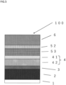
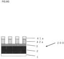
- FIG. 3 is a cross-sectional view showing an example of a reflective photomask 200 of the present invention.
- the reflective photomask includes a substrate 1, a multilayer reflective film 2 formed on the substrate 1 so as to be in contact with the substrate 1 and reflecting exposure light that is extreme ultraviolet region light, a protective film 3 formed on the multilayer reflective film 2 so as to be in contact with the multilayer reflective film 2 and protecting the multilayer reflective film, and a light absorbing film pattern (a circuit pattern or a photomask pattern) 4a formed on the protective film 3 so as to be in contact with the protective film 3 and absorbing exposure light, and the light absorbing film pattern 4a includes an oxide layer pattern 41a of the light absorbing film and an absorbing layer pattern 42a of the light absorbing film.
- the multilayer reflective film 2, the protective film 3, and the light absorbing film pattern 4a are laminated in this order from the substrate 1.
- the light absorbing film pattern 4a includes an oxide layer pattern 41a of the light absorbing film and an absorbing layer pattern 42a of the light absorbing film.
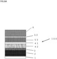
- FIG. 5 is a cross-sectional view showing an example of a third aspect of a reflective photomask blank of the present invention.
- the reflective photomask blank 100 includes a substrate 1, a multilayer reflective film 2 formed on the substrate 1 so as to be in contact with the substrate 1 and reflecting exposure light that is extreme ultraviolet region light, a protective film 3 formed on the multilayer reflective film 2 so as to be in contact with the multilayer reflective film 2 and protecting the multilayer reflective film 2, a light absorbing film 4 formed on the protective film 3 so as to be in contact with the protective film 3 and absorbing the exposure light, and an upper hard mask layer 52 of a second layer and a lower hard mask layer 53 of the second layer that are formed on the light absorbing film 4 so as to be in contact with the light absorbing film 4 and function as hard masks when the light absorbing film 4 is patterned by dry etching.
- the light absorbing film 4 has an oxide layer 41 of the light absorbing film provided on a side that is spaced from the substrate, and an absorbing layer 42 of the light
- the multilayer reflective film 2, the protective film 3, the absorbing layer 42 of the light absorbing film, the oxide layer 41 of the light absorbing film, the lower hard mask layer 53 of the second layer, the upper hard mask layer 52 of the second layer, and the resist film 6 are laminated in this order from the substrate 1.
- the type and size of the substrate are not particularly limited, and the substrates of the reflective photomask blank and the reflective photomask may or may not be transparent at an exposure wavelength.
- a glass substrate such as a quartz substrate can be used.
- a so-called 6025 substrate having a size of 6 inch square and a thickness of 0.25 inches defined in the SEMI standard is preferable.
- the 6025 substrate is usually described as a substrate having a size of 152 mm square and a thickness of 6.35 mm.
- a back surface film may be formed on a back surface of the substrate (a surface opposite to a surface on which the multilayer reflective film or the like is formed) in order to promote fixing of the substrate by the electrostatic chuck.
- the multilayer reflective film is a film that reflects exposure light that is extreme ultraviolet region light.
- the multilayer reflective film is preferably formed in contact with the substrate.
- the extreme ultraviolet region light is called EUV light
- a wavelength of the EUV light is 13 to 14 nm
- the EUV light is usually light having a wavelength of about 13.5 nm.
- a material constituting the multilayer reflective film is preferably a material that has resistance to dry etching (chlorine-based dry etching) using chlorine-based gas (for example, only Cl 2 gas or mixed gas of Cl 2 gas and O 2 gas) and can be removed by dry etching (fluorine-based dry etching) using fluorine-based gas (for example, CF 4 gas or SF 6 gas) .
- the material constituting the multilayer reflective film include molybdenum (Mo) and silicon (Si).
- Mo molybdenum
- Si silicon
- a thickness of the multilayer reflective film is preferably 200 nm or more and particularly 220 nm or more, and is preferably 340 nm or less and particularly 280 nm or less.
- a thickness of the molybdenum (Mo) layer is preferably 1 nm or more and particularly 2 nm or more, and is preferably 5 nm or less and particularly 4 nm or less.
- a thickness of the silicon (Si) layer is preferably 2 nm or more and particularly 3 nm or more, and is preferably 6 nm or less and particularly 5 nm or less.
- the protective film is a film for protecting the multilayer reflective film.
- the protective film is preferably formed in contact with the multilayer reflective film.
- the protective film is provided to protect the multilayer reflective film, for example, in cleaning in processing into the reflective photomask, correction of the reflective photomask, or the like.
- the protective film preferably has a function of protecting the multilayer reflective film when the light absorbing film is patterned by etching and preventing oxidation of the multilayer reflective film.
- a material constituting the protective film is preferably a material having an etching characteristic different from that of the light absorbing film, and specifically, is a material having resistance to chlorine-based dry etching, and is preferably a material having resistance to cleaning containing sulfuric acid and cleaning containing alkali.
- the material constituting the protective film include a material containing ruthenium (Ru).
- the protective film may be formed of a ruthenium compound containing one or more selected from Mo, Nb, Zr, Y, B, Ti, and La in order to have resistance to chlorine-based dry etching, chlorine-based dry etching containing oxygen, cleaning containing sulfuric acid, and cleaning containing alkali.
- the protective film may be a single layer film, a multilayer film (for example, a film including 2 to 4 layers), or a film having a gradient composition.
- a thickness of the protective film is preferably 1 nm or more and preferably 20 nm or less.
- the light absorbing film includes an oxide layer of the light absorbing film and an absorbing layer of the light absorbing film, and the absorbing layer of the light absorbing film is a film that absorbs exposure light that is extreme ultraviolet region light.
- the absorbing layer of the light absorbing film is preferably formed in contact with the protective film.
- the absorbing layer of the light absorbing film is preferably formed of a material that has resistance to chlorine-based dry etching containing oxygen and can be removed by chlorine-based dry etching containing no oxygen and fluorine-based dry etching.
- the absorbing layer of the light absorbing film is preferably formed of a material containing tantalum (Ta).
- the material containing tantalum in the absorbing layer of the light absorbing film include elemental tantalum (Ta) and a tantalum compound containing tantalum (Ta), and one or more selected from nitrogen (N), boron (B), and the like.
- a material (Ta) formed of tantalum a material (TaN) formed of tantalum and nitrogen, a material (TaB) formed of tantalum and boron, and a material (TaNB) formed of tantalum, nitrogen, and boron.
- the tantalum compound may contain a trace amount of oxygen (O).
- the light absorbing film may be a single layer film, a multilayer film (for example, a film including 2 to 4 layers), or a film having a gradient composition.
- a thickness of the absorbing layer of the light absorbing film is preferably 30 nm or more, more preferably 40 nm or more, and particularly 50 nm or more, and is preferably 100 nm or less, more preferably 80 nm or less, and particularly 74 nm or less.
- the oxide layer of the light absorbing film is a film that reduces light reflectance.
- the oxide layer of the light absorbing film is preferably formed in contact with the absorbing layer of the light absorbing film.
- the oxide layer of the light absorbing film is preferably formed of a material that has resistance to chlorine-based dry etching and can be removed by fluorine-based dry etching.
- the oxide layer of the light absorbing film is preferably formed of a material containing tantalum (Ta) and oxygen (O).
- the material containing tantalum and oxygen may be a tantalum compound containing a material selected from nitrogen (N), boron (B), and the like.
- a material (TaO) formed of tantalum and oxygen examples include a material (TaO) formed of tantalum and oxygen, a material (TaON) formed of tantalum, oxygen, and nitrogen, a material (TaOB) formed of tantalum, oxygen, and boron, and a material (TaONB) formed of tantalum, oxygen, nitrogen, and boron.
- the oxide layer of the light absorbing film may be a single layer film, a multilayer film (for example, a film including 2 to 4 layers), or a film having a gradient composition.
- a thickness of the oxide layer of the light absorbing film is preferably 1 nm or more and particularly 2 nm or more, and is preferably 10 nm or less and particularly 5 nm or less, in order to reduce the light reflectance.
- an oxygen content ratio is preferably 5% or less and is particularly preferably 3% or less.
- the oxygen content ratio is preferably 15% or more and is particularly preferably 18% or more.
- the oxide layer 41 of the light absorbing film is a layer that functions as an etching mask (hard mask) in chlorine-based dry etching containing no oxygen for the absorbing layer 42 of the light absorbing film (see FIG. 6G ), and when the absorbing layer 42 of the light absorbing film is subjected to chlorine-based dry etching containing no oxygen under one condition (predetermined same condition), a ratio of an etching rate (nm/sec) of the absorbing layer 42 of the light absorbing film to an etching rate (nm/sec) of the oxide layer 41 of the light absorbing film is preferably 45 or more and particularly 70 or more.
- the etching rate (nm/sec) By setting the etching rate (nm/sec) to such a ratio, when the absorbing layer pattern of the light absorbing film is formed using the lower hard mask layer pattern of the second layer and the oxide layer pattern of the light absorbing film as the hard masks using chlorine-based dry etching containing no oxygen (see FIG. 6G ), after the lower hard mask layer pattern of the second layer disappears, the etching rate of the oxide layer pattern of the light absorbing film is slow, and thus, it is possible to perform long-term over-etching on the absorbing layer pattern of the light absorbing film, and the stability of the CD can be improved. In addition, this increases the process window and allows more dry etching conditions to be used.
- the hard mask of the present invention includes a multilayer including a first layer provided on a side furthest from the substrate and a second layer provided on a side other than the side furthest from the substrate.
- the hard mask is not limited to one including two layers, and may include three or more layers, for example, three layers, four layers, or five layers.
- a film formed of a material having strong cleaning resistance or a film formed of a material having high adhesion to a resist can be used.
- the second layer is preferably provided on a side closest to the substrate.
- the first layer of the hard mask is formed of a material that has resistance to chlorine-based dry etching and can be removed by fluorine-based dry etching. Due to such dry etching characteristics, the first layer functions as an etching mask in etching of the second layer, the oxide layer of the light absorbing film, and the absorbing layer of the light absorbing film.
- a material of the first layer a material containing silicon (Si) and containing no chromium (Cr) is suitable.
- the second layer of the hard mask includes the upper hard mask layer 2A of the second layer and the lower hard mask layer 2B of the second layer.
- the upper hard mask layer 2A of the second layer is formed of a material that has resistance to chlorine-based dry etching and can be removed by fluorine-based dry etching.
- the lower hard mask layer 2B of the second layer is formed of a material that has resistance to chlorine-based dry etching containing oxygen and can be removed by chlorine-based dry etching containing no oxygen and fluorine-based dry etching.
- the upper hard mask layer 2A of the second layer functions as an etching mask in chlorine-based dry etching containing no oxygen in the absorbing layer of the light absorbing film.
- the upper hard mask layer 2A of the second layer is preferably formed of a material containing tantalum (Ta) and oxygen (O).
- the material containing tantalum and oxygen may be a tantalum compound containing a material selected from nitrogen (N), boron (B), and the like. Examples of such a material include a material (TaO) formed of tantalum and oxygen, a material (TaON) formed of tantalum, oxygen, and nitrogen, a material (TaOB) formed of tantalum, oxygen, and boron, and a material (TaONB) formed of tantalum, oxygen, nitrogen, and boron.
- the upper hard mask layer 2A of the second layer may be a single layer film, a multilayer film (for example, a film including 2 to 4 layers), or a film having a gradient composition.
- the upper hard mask layer 2A of the second layer is preferably formed of a material that has resistance to chlorine-based dry etching and can be removed by fluorine-based dry etching.
- the lower hard mask layer 2B of the second layer is preferably formed in contact with the upper hard mask layer 2A of the second layer.
- the lower hard mask layer 2B of the second layer is preferably formed of a material containing tantalum (Ta).
- the material containing tantalum include elemental tantalum (Ta) and a tantalum compound containing tantalum (Ta), and one or more selected from nitrogen (N), boron (B), and the like.
- a material (Ta) formed of tantalum a material (TaN) formed of tantalum and nitrogen, a material (TaB) formed of tantalum and boron, and a material (TaNB) formed of tantalum, nitrogen, and boron.
- the lower hard mask layer 2B of the second layer may be a single layer film, a multilayer film (for example, a film including 2 to 4 layers), or a film having a gradient composition.
- the lower hard mask layer 2B of the second layer is preferably formed of a material that has resistance to chlorine-based dry etching containing oxygen and can be removed by chlorine-based dry etching containing no oxygen and fluorine-based dry etching.
- the first layer is a layer in contact with the resist film.
- the first layer is a film that functions as an etching mask (hard mask) for the lower hard mask layer 2B of the second layer in chlorine-based dry etching containing no oxygen.
- the first layer is preferably formed of a material that has resistance to chlorine-based dry etching and can be removed by fluorine-based dry etching.
- a material of the first layer may contain one or more selected from oxygen (O), nitrogen (N), and carbon (C) in addition to silicon, and in particular, a material containing silicon and one or more selected from oxygen, nitrogen, and carbon is preferable.
- a silicon content ratio is less than 100 atom%, but is preferably 80 atom% or less and particularly 60 atom% or less. The lower the silicon content ratio, the higher the etching rate (etching speed) in fluorine-based dry etching of the first layer. On the other hand, a lower limit of the silicon content ratio is usually 20 atom% or more, and preferably 30 atom% or more.
- the material of the first layer preferably contains nitrogen, and silicon nitride (SiN) composed of silicon and nitrogen is particularly preferable.
- the silicon content ratio is preferably 20 atom% or more and particularly 30 atom% or more, and is preferably 80 atom% or less and particularly 60 atom% or less.
- a nitrogen content ratio is preferably 80 atom% or less and particularly 55 atom% or less.
- a lower limit of the nitrogen content ratio is not particularly limited, and is preferably 20 atom% or more and particularly 30 atom% or more.
- the material of the first layer preferably contains oxygen, and silicon oxide (SiO) composed of silicon and oxygen is particularly preferable.
- the silicon content ratio is preferably 20 atom% or more and particularly 30 atom% or more, and is preferably 80 atom% or less and particularly 60 atom% or less.
- the oxygen content ratio is preferably 20 atom% or more and particularly 25 atom% or more, and is preferably 80 atom% or less and particularly 68 atom% or less.
- the material of the first layer preferably contains nitrogen as well as oxygen, and silicon nitride oxide (SiON) composed of silicon, oxygen, and nitrogen is particularly preferable.
- the silicon content ratio is preferably 20 atom% or more and particularly 30 atom% or more, and is preferably less than 80 atom% and particularly 60 atom% or less.
- the oxygen content ratio is preferably more than 0 atom% and less than 80 atom%, and particularly 68 atom% or less.
- the nitrogen content ratio is preferably more than 0 atom% and less than 80 atom%, and particularly 55 atom% or less.
- the first layer is patterned by fluorine-based dry etching using a resist pattern formed in contact with the first layer as an etching mask, but the thinner the first layer, the shorter the etching time, and thus, a thickness of the first layer is preferably 12 nm or less and particularly 10 nm or less.
- the thickness of the first layer is preferably 2 nm or more and particularly 4 nm or more.
- the material containing silicon but no chromium has resistance to chlorine-based dry etching containing no oxygen for the lower hard mask layer 2B of the second layer, and the first layer pattern functions as an etching mask in chlorine-based dry etching containing no oxygen for the lower hard mask layer 2B of the second layer. Furthermore, since the first layer can be etched by fluorine-based dry etching that does not require long-term over-etching, the thickness of the resist film used for etching the first layer can be reduced.
- a material containing oxygen together with silicon and containing no chromium preferably a material containing each element in the content described above, and more preferably a material having a composition having a relatively high oxygen content has high adhesion to a resist film, and is hardly dissolved in a mixed solution of sulfuric acid and aqueous hydrogen peroxide, ammonia added water, or the like as compared with a material containing chromium, and it is possible to stably maintain optical characteristics required for defect inspection and the like.
- a material containing oxygen together with silicon and containing no chromium preferably a material containing each element in the content described above, and more preferably a material having a composition having a relatively high oxygen content has a chemically stable surface state as compared with a material containing tantalum, and the stability of the CD is improved when a resist pattern is produced.
- the first layer is formed on the side of the etching mask film that is farthest from the substrate, such that even a line pattern such as a fine assist pattern is hardly collapsed due to the impact by the developer or the impact of by the pure water during the rinsing process in the development process of resist pattern formation, an excellent resist pattern can be formed, and high resolution can be stably obtained.
- the material of the first layer, the material of the upper hard mask layer 2A of the second layer, and the material of the lower hard mask layer 2B of the second layer are materials that can be removed by fluorine-based dry etching
- the first layer pattern, the upper hard mask layer pattern of the second layer, and the lower hard mask layer pattern of the second layer can be removed simultaneously with formation of the absorbing layer pattern of the light absorbing film in fluorine-based dry etching when the oxide layer pattern of the light absorbing film and the absorbing layer pattern of the light absorbing film are formed.
- the total etching clear time when the first layer and the upper hard mask layer 2A of the second layer are subjected to fluorine-based dry etching under one condition is shorter than the total etching clear time of 1/2 of the thicknesses of the oxide layer of the light absorbing film and the absorbing layer of the light absorbing film (under the same conditions as the fluorine-based dry etching of the first layer and the upper hard mask layer 2A of the second layer).
- the total etching clear time when the upper hard mask layer 2A of the second layer is subjected to fluorine-based dry etching under one condition is shorter than the etching clear time of 1/2 of the thicknesses of the oxide layer of the light absorbing film and the absorbing layer of the light absorbing film (under the same conditions as the fluorine-based dry etching of the upper hard mask layer 2A of the second layer).
- a ratio of an etching rate (nm/sec) of the first layer to an etching rate (nm/sec) of the absorbing layer of the light absorbing film is preferably 0.4 or more and particularly 0.7 or more, but is preferably 2.0 or less and particularly 1.2 or less.
- a difference between the thickness of the first layer, and the total thickness of the oxide layer of the light absorbing film and the absorbing layer of the light absorbing film is preferably 30 nm or more, particularly 40 nm or more, and further particularly 44 nm or more.
- a ratio of an etching rate (nm/sec) of the lower hard mask layer 2B of the second layer to an etching rate (nm/sec) of the absorbing layer of the light absorbing film is preferably 0.7 or more and particularly 0.8 or more, but is preferably 1.3 or less and particularly 1.2 or less.
- the ratio of the etching rate (nm/sec) of the lower hard mask layer 2B of the second layer to the etching rate (nm/sec) of the absorbing layer of the light absorbing film is preferably 0.7 or more and particularly 0.8 or more, but is preferably 1.3 or less and particularly 1.2 or less.
- the second layer includes the upper hard mask layer 2A of the second layer and the lower hard mask layer 2B of the second layer, the upper hard mask layer 2A of the second layer is a layer that functions to stabilize a surface layer of the second layer formed of a material containing chemically active tantalum, and the lower hard mask layer 2B of the second layer is a layer that functions as an etching mask (hard mask) in chlorine-based dry etching containing no oxygen for the light absorbing film.
- etching mask hard mask
- the thickness of the second layer is preferably 8 nm or more and particularly 10 nm or more, and is preferably 30 nm or less and particularly 20 nm or less, in order to shorten the clear time of etching.
- the material containing tantalum can be removed by chlorine-based dry etching containing no oxygen.
- chlorine-based dry etching containing no oxygen side etching hardly occurs on a side wall of a pattern, and a pattern shape is perpendicular to a substrate, as compared with chlorine-based dry etching containing oxygen.
- large side etching occurs in the line pattern, the dimension near the center of the pattern with respect to the vertical direction is reduced with respect to the upper side and the lower side with respect to the vertical direction of the pattern by the side etching from both sides, and the pattern is easily broken during dry etching, and as a result, resolution is deteriorated.
- the material containing tantalum can be removed by fluorine-based dry etching, and the upper hard mask layer 2A of the second layer formed of tantalum containing oxygen is removed simultaneously when the oxide layer of the light absorbing film and parts of the absorbing layer of the light absorbing film are etched by fluorine-based dry etching.
- a part of the lower hard mask layer 2B of the second layer containing tantalum is removed at the same time when a part of the absorbing layer of the light absorbing film is etched by fluorine-based dry etching.
- chlorine-based dry etching containing no oxygen is performed on the absorbing layer of the remaining light absorbing film to form an absorbing layer pattern of the light absorbing film, and at the same time, a part of the lower hard mask layer 2B of the second layer remaining as described above is removed.
- the oxide layer of the light absorbing film includes the oxide layer containing oxygen
- the light absorbing film has resistance to chlorine etching containing no oxygen, and functions as an etching prevention film when a part of the lower hard mask layer 2B of the second layer is removed.
- chlorine etching containing no oxygen is performed when the absorbing layer pattern of the light absorbing film is formed, the thickness of the protective film having resistance to chlorine etching containing no oxygen does not decrease.
- Chlorine-based dry etching containing oxygen has high reactivity to ruthenium and has a higher etching rate than chlorine-based dry etching containing no oxygen. Therefore, when the protective film is etched for a long time by chlorine-based dry etching containing oxygen, the protective film is completely removed, and the function of the protective film is lost.
- the upper hard mask layer 2A of the second layer and the lower hard mask layer 2B of the second layer are provided together with the first layer in the etching mask film, such that high resolution can be obtained and the film thickness of the protective film can be maintained.
- the upper hard mask layer 2A of the second layer is preferably tantalum oxynitride containing tantalum, oxygen, and nitrogen
- the lower hard mask layer 2B of the second layer is preferably tantalum nitride containing tantalum and nitrogen.
- an oxygen content ratio is preferably 5% or less and is particularly preferably 3% or less.
- the oxygen content ratio is preferably 15% or more and is particularly preferably 18% or more.
- the upper hard mask layer 2A of the second layer is a layer that functions as an etching mask (hard mask) in chlorine-based dry etching containing no oxygen for the lower hard mask layer 2B of the second layer, and when the lower hard mask layer 2B of the second layer is subjected to chlorine-based dry etching containing no oxygen under the same conditions, it is preferable that the ratio of the etching rate (nm/sec) of the lower hard mask layer 2B of the second layer to the etching rate (nm/sec) of the upper hard mask layer 2A of the second layer is 45 or more, and particularly 70 or more.
- the etching rate (nm/sec) By setting the etching rate (nm/sec) to such a ratio, as illustrated in FIG. 6E , when the lower hard mask layer pattern of the second layer is formed using the upper hard mask layer pattern of the second layer as a hard mask using chlorine-based dry etching containing no oxygen, the etching rate of the upper hard mask layer pattern of the second layer is slow, and thus, it is possible to perform long over-etching on the lower hard mask layer pattern of the second layer, which improves CD stability. In addition, this increases the process window and allows more dry etching conditions to be used.
- the absorbing layer of the light absorbing film can be removed simultaneously when being removed by dry etching containing no oxygen.
- the resist film may be an electron beam resist drawn by an electron beam or a photoresist drawn by light, and a chemically amplified resist is preferable.
- the chemically amplified resist may be a positive type or a negative type, and examples thereof include a chemically amplified resist containing a base resin such as a hydroxystyrene-based resin or a (meth)acrylic acid-based resin, and an acid generator, and a crosslinking agent, a quencher, a surfactant, or the like that is added as necessary.
- the thickness of the resist film formed on the first layer of the present invention can be reduced as described above.
- the thickness of the resist film is preferably 80 nm or less from the viewpoint of making the resist pattern for forming a fine assist pattern less prone to collapse by the impact by the developer or the impact by the pure water during the rinsing process in the development process of resist pattern formation, and is preferably 70 nm or less and particularly 60 nm or less from the viewpoint of preferably forming a line pattern such as an assist pattern having a width of about 25 nm and particularly about 20 nm.
- a lower limit of the thickness of the resist film is a thickness that functions as an etching mask in etching of the first layer, may be a thickness at which the resist pattern remains on the entire pattern of the first layer after etching, is not particularly limited, and is preferably 15 nm or more, and particularly 20 nm or more.
- the multilayer reflective film, the protective film, the light absorbing film, and the first layer and the upper hard mask layer 2A of the second layer and the lower hard mask layer 2B of the second layer of the present invention are not particularly limited, and are preferably formed by a sputtering method because these films have excellent controllability and easily form films having predetermined characteristics.
- DC sputtering, RF sputtering, and the like can be applied as the sputtering method, and there is no particular limitation.
- a molybdenum target and a silicon target can be used as the sputtering target.
- a film formed of a material containing ruthenium is formed as the protective film
- a ruthenium target can be used as the sputtering target.
- a film formed of a material containing tantalum is formed as the light absorbing film
- a tantalum target can be used as the sputtering target.
- a silicon target can be used as the sputter target.
- Power supplied to the sputtering target may be appropriately set depending on the size of the sputtering target, cooling efficiency, ease of film formation control, and the like, and usually, power per area of a sputtering surface of the sputtering target may be 50 to 3,000 W/cm 2 .
- a rare gas such as helium gas (He gas), neon gas (Ne gas), or argon gas (Ar gas) is used, and when each of the film and the layer included in the film is formed using only the target element, only rare gas may be used as the sputtering gas. In the case of formation with only the target element, only rare gas may be used as the sputtering gas.
- the sputtering is preferably reactive sputtering.
- the sputtering gas for reactive sputtering rare gases such as helium gas (He gas), neon gas (Ne gas), argon gas (Ar gas), and reactive gases are used.
- oxygen gas (O 2 gas) may be used as the reactive gas in the case where each of the film and the layer is formed of a material containing oxygen
- nitrogen gas (N 2 gas) may be used as the reactive gas in the case where each of the film and the layer is formed of a material containing nitrogen.
- the reactive gas may be appropriately selected and used from oxygen gas (O 2 gas), nitrogen gas (N 2 gas), and nitrogen oxide gas such as nitrogen monoxide gas (NO gas), nitrogen dioxide gas (NO 2 gas), or nitrous oxide gas (N 2 O gas).
- oxygen gas O 2 gas
- nitrogen gas N 2 gas
- nitrogen oxide gas such as nitrogen monoxide gas (NO gas), nitrogen dioxide gas (NO 2 gas), or nitrous oxide gas (N 2 O gas).
- gas containing carbon such as methane gas (CH 4 ), carbon monoxide gas (CO gas), or carbon dioxide gas (CO 2 gas) may be used as the reactive gas
- gas containing carbon such as methane gas (CH 4 ), carbon monoxide gas (CO gas), or carbon dioxide gas (CO 2 gas)
- the film is formed of a material containing oxygen, nitrogen, and carbon, for example, oxygen gas (O 2 gas), nitrogen gas (N 2 gas), and carbon dioxide gas (CO 2 ) may be simultaneously used as the reactive gas.
- each of the film and the layer included in the film may be appropriately set in consideration of film stress, chemical resistance, cleaning resistance, and the like, and the chemical resistance is usually improved by setting the pressure to 0.01 Pa or more, particularly 0.03 Pa or more and 1 Pa or less, and more particularly 0.3 Pa or less.
- each gas flow rate may be appropriately set so as to have a desired composition, and may be usually 0.1 to 100 sccm.
- the substrate or the substrate and the film formed on the substrate may be subjected to a heat treatment.
- a heat treatment infrared heating, resistance heating, and the like can be applied, and conditions of the treatment are not particularly limited.
- the heat treatment can be performed, for example, in a gas atmosphere containing oxygen.
- a concentration of the gas containing oxygen is not particularly limited, and can be, for example, 1 to 100 vol% in the case of oxygen gas (O 2 gas).
- a temperature of the heat treatment is preferably 200°C or higher and particularly 400°C or higher.
- the film formed on the substrate, particularly the first layer may be subjected to an ozone treatment, a plasma treatment, or the like, and the conditions of the treatment are not particularly limited. Any treatment can be performed for the purpose of increasing the oxygen concentration of the surface part of the film, and in this case, the treatment conditions may be appropriately adjusted so as to have a predetermined oxygen concentration.
- the oxygen concentration of the surface part of the film can be increased by adjusting a ratio of a rare gas in the sputtering gas to a gas containing oxygen (oxidizing gas) such as oxygen gas (O 2 gas), carbon monoxide gas (CO gas), or carbon dioxide gas (CO 2 gas).
- oxygen gas oxygen gas (O 2 gas), carbon monoxide gas (CO gas), or carbon dioxide gas (CO 2 gas).
- the first layer may be a single layer film, a multilayer film (for example, a film including 2 to 4 layers), or a film having a gradient composition.
- the first layer in a case where a content of silicon is low, a content of nitrogen or oxygen, or a content of nitrogen and oxygen is high, the etching rate by the fluorine-based gas is increased, and the film thickness of the resist film can be reduced, but the surface roughness of the film surface layer is reduced, the adhesion between the first layer and the resist film is poor, and the resolution of the resist pattern is deteriorated.
- the etching rate by the fluorine-based gas is decreased, and the film thickness of the resist film cannot be reduced, but the surface roughness of the film surface layer is increased, the adhesion between the first layer and the resist film is excellent, and the resolution of the resist pattern is improved.
- a film in which a content of silicon is high, a content of nitrogen or oxygen, or a content of nitrogen and oxygen is low, a content of silicon is low toward the substrate direction, and a content of nitrogen or oxygen, or a content of nitrogen and oxygen is high is preferable because adhesion with the resist film is excellent, and the etching rate can be fast.
- a cleaning process may be performed in order to remove defects present on the surface of the substrate or the film formed on the substrate.
- the cleaning can be performed using one or both of ultrapure water and functional water that is ultrapure water containing ozone gas, hydrogen gas, and the like.
- cleaning may be further performed using one or both of ultrapure water and functional water. The cleaning can be performed while performing irradiation with ultrasonic waves as necessary, and UV light irradiation can also be combined.
- the method for forming the resist film (coating of the resist) is not particularly limited, and a known method can be applied.
- a method for manufacturing a reflective photomask from a reflective photomask blank according to a first aspect of the present invention will be described with reference to the drawings.
- a method for manufacturing a reflective photomask from a reflective photomask blank of the present invention it is possible to apply a method in which a resist pattern is formed from a resist film, dry etching using fluorine-based gas (fluorine-based dry etching) or dry etching using chlorine-based gas (chlorine-based dry etching) is applied to a film or a layer under the film using the resist pattern as an etching mask according to a material forming the film or the layer, the pattern is formed, and the pattern is removed at an appropriate time.
- the resist film and the resist pattern can be removed by sulfuric acid hydrogen peroxide.
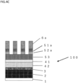
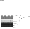
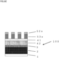
- FIGS. 4A to 4G are cross-sectional views for explaining a process of manufacturing a reflective photomask from a reflective photomask blank of the present invention.
- a resist film 6 is formed in contact with a side of a reflective photomask blank 100 of the first aspect that is spaced from a substrate 1 (that is, in contact with a first layer 51) (step (A)).
- the resist film 6 is patterned to form a resist film pattern 6a (step (B)).
- a first layer 51 and an upper hard mask layer 2A of a second layer are simultaneously patterned by dry etching using fluorine-based gas to form a first layer pattern 51a and an upper hard mask layer pattern 52a of the second layer
- step (D) the resist pattern 6a is removed (step (D)).
- a lower hard mask layer 2B of the second layer is patterned by dry etching using chlorine-based gas containing no oxygen to form a lower hard mask layer pattern 53a of the second layer (step (E)).
- an oxide layer 41 of a light absorbing film and parts of an absorbing layer 42 of the light absorbing film are patterned by fluorine-based dry etching to form an oxide layer pattern 41a and an absorbing layer pattern 42a of the light absorbing film.
- the absorbing layer 42 of the light absorbing film is not entirely etched, and a part thereof remains (step (F)).
- the oxide layer 41 of the light absorbing film and parts of the absorbing layer 42 of the light absorbing film are patterned by fluorine-based dry etching, the first layer pattern 51a, the upper hard mask layer pattern 52a of the second layer, and parts of the lower hard mask layer pattern 53a of the second layer are simultaneously removed. After the dry etching, a part of the lower hard mask layer pattern 53a remains on the oxide layer pattern 41a of the light absorbing film.
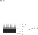
- the absorbing layer pattern 42a of the light absorbing film remaining in FIG. 4F is removed by dry etching using chlorine-based gas containing no oxygen (step (G)).
- the remaining lower hard mask layer pattern 53a of the second layer is simultaneously removed and held by chlorine-based dry etching containing no oxygen.
- the oxide film pattern 41a of the light absorbing film has resistance to chlorine-based dry etching containing no oxygen, and thus functions as an etching prevention film.
- a resist film is formed in advance, and thus, the step (A) can be omitted, and the steps (B) to (G) may be performed.
- a thin resist film is formed on a reflective photomask blank so as to have a thickness of, for example, 60 nm or less, or a light absorbing film is patterned from a reflective photomask blank in which a thin resist film having a thickness of, for example, 60 nm or less is formed, such that it is possible to obtain a reflective photomask in which a pattern of a light absorbing film including a line pattern such as an assist pattern that is excellent even when a line width is 25 nm or less (25 nm or less than 25 nm), and particularly 20 nm or less (20 nm or less than 20 nm) is formed. Furthermore, as in the step of FIG.
- a lower limit of a width of the line pattern such as the assist pattern formed in the light absorbing film pattern of the reflective photomask is usually 10 nm or more.
- FIG. 5 is a cross-sectional view for explaining a process of manufacturing a reflective photomask from the reflective photomask blank according to a third aspect of the present invention.
- a resist film 6 is formed in contact with a side of a reflective photomask blank 100 of the third aspect that is spaced from a substrate 1 (that is, in contact with an upper hard mask layer 2A of a second layer) (step (A)).
- the resist film 6 is patterned to form a resist film pattern 6a (step (B)).
- an upper hard mask layer 2A of a second layer is patterned by dry etching using fluorine-based gas to form an upper hard mask layer pattern 52a of the second layer
- step (D) the resist pattern 6a is removed (step (D)).
- a lower hard mask layer 2B of the second layer is patterned by dry etching using chlorine-based gas containing no oxygen to form the lower hard mask layer pattern 53a of the second layer (step (E)).
- an oxide layer 41 of a light absorbing film and an parts of absorbing layer 42 of the light absorbing film are patterned by fluorine-based dry etching to form an oxide layer pattern 41a and an absorbing layer pattern 42a of the light absorbing film.
- the absorbing layer 42 of the light absorbing film is not entirely etched, and a part thereof remains (step (F)).
- the oxide layer 41 of the light absorbing film and parts of the absorbing layer 42 of the light absorbing film are patterned by fluorine-based dry etching
- the upper hard mask layer pattern 52a of the second layer and parts of the lower hard mask layer pattern 53a of the second layer are simultaneously removed. After the dry etching, a part of the lower hard mask layer pattern 53a remains on the oxide layer pattern 41a of the light absorbing film.
- the absorbing layer pattern 42a of the light absorbing film remaining in FIG. 6F is removed by dry etching using chlorine-based gas containing no oxygen (step (G)).
- the remaining lower hard mask layer pattern 53a of the second layer is simultaneously removed and held by chlorine-based dry etching containing no oxygen.
- the oxide film pattern 41a of the light absorbing film has resistance to chlorine-based dry etching containing no oxygen, and thus functions as an etching prevention film.
- the step (A) can be omitted, and the steps (B) to (G) may be performed.
- a thin resist film is formed on a reflective photomask blank that does not include a first layer so as to have a thickness of, for example, 60 nm or less, or a light absorbing film is patterned from a reflective photomask blank in which a thin resist film having a thickness of, for example, 60 nm or less is formed, such that it is possible to obtain a reflective photomask, in which a pattern of a light absorbing film including a line pattern such as an assist pattern that is excellent even when a line width is 25 nm or less (25 nm or less than 25 nm), and particularly 20 nm or less (20 nm or less than 20 nm), is formed. Furthermore, as in the step of FIG. 6G , the protective film 3 is exposed to dry etching using chlorine-based gas containing no oxygen, and there is no damage and the thickness of the film does not decrease.
- a lower limit of a width of the line pattern such as the assist pattern formed in the light absorbing film pattern of the reflective photomask is usually 10 nm or more.
- a multilayer reflective film, a protective film, a light absorbing film, and a hard mask including a first layer and a second layer were sequentially laminated on a quartz substrate having a size of 152 mm square and a thickness of about 6 mm to manufacture a reflective photomask blank (reflective photomask blank of a first aspect) as illustrated in FIG. 1 .
- a molybdenum target and a silicon target were used as targets, argon gas was used as sputtering gas, power applied to the target was adjusted, a flow rate of the sputtering gas was adjusted, and sputtering by the molybdenum target and sputtering by the silicon target were alternately performed to form a multilayer reflective film 2 that is a laminated film (thickness: 280 nm) in which a molybdenum (Mo) layer and a silicon (Si) layer having a reflectance for light having a wavelength of 13.5 nm of 65% were alternately laminated on the quartz substrate that is a substrate 1.
- a total of 40 layers were formed by combining molybdenum (Mo) layers and silicon layers.
- sputtering was performed by using ruthenium as a target, using argon gas as sputtering gas, adjusting power applied to the target, and adjusting a flow rate of the sputtering gas to form a ruthenium (Ru) film (thickness: 5 nm) on the multilayer reflective film as a protective film 3 formed of a material containing ruthenium.
- Ru ruthenium
- sputtering was performed by using a tantalum target as a target, using argon gas and nitrogen gas as sputtering gas, adjusting power applied to the target, and adjusting a flow rate of the sputtering gas to form a tantalum nitride (TaN) film (thickness: 65 nm) on the protective film as an absorbing layer 42 of a light absorbing film formed of a material containing tantalum.
- TaN tantalum nitride
- sputtering was performed by using a tantalum target as a target, using argon gas and oxygen gas as sputtering gas, adjusting power applied to the target, and adjusting a flow rate of the sputtering gas to form a tantalum oxide (TaO) film (thickness: 3 nm) on the absorbing layer 42 of the light absorbing film as an oxide layer 41 of the light absorbing film formed of a material containing tantalum.
- TaO tantalum oxide
- sputtering was performed by using a tantalum target as a target, using argon gas and nitrogen gas as sputtering gas, adjusting power applied to the target, and adjusting a flow rate of the sputtering gas to form a tantalum nitride (TaN) film (thickness: 10 nm) on the oxide layer of the light absorbing film as a lower hard mask layer 53 of the second layer formed of a material containing tantalum.
- TaN tantalum nitride
- sputtering was performed by using a tantalum target as a target, using argon gas and oxygen gas as sputtering gas, adjusting power applied to the target, and adjusting a flow rate of the sputtering gas to form a tantalum oxynitride (TaON) film (thickness: 3 nm) on the lower hard mask layer 53 of the second layer as an upper hard mask layer 52 of the second layer formed of a material containing tantalum.
- TaON tantalum oxynitride
- sputtering was performed by using a silicon target as a target, using argon gas and nitrogen gas as sputtering gas, adjusting power applied to the target, and adjusting a flow rate of the sputtering gas to form a silicon nitride (SiN) layer (thickness: 10 nm) on the second layer as a first layer 51 formed of a material containing silicon but no chromium and obtain a reflective photomask blank.
- SiN silicon nitride
- composition and thickness of the first layer 51, the thickness of the upper hard mask layer 52 of the second layer, the thickness of the lower hard mask layer 53 of the second layer, the material of the lower hard mask layer 53 of the second layer, the thickness of the oxide layer 41 of the light absorbing film, and the thickness of the absorbing layer 42 of the light absorbing film are shown in Table 1. Note that the composition was measured using an X-ray photoelectron spectrometer, and the thickness was measured using an X-ray diffractometer (the same applies hereinafter).
- a reflective photomask blank was obtained in the same manner as in Example 1, except that the formation of the first layer 51 was changed as follows and the thickness of the lower hard mask layer 53 of the second layer was changed.
- Sputtering was performed on the first layer 51 by using a silicon target as a target, using argon gas and oxygen gas as sputtering gas, adjusting power applied to the target, and adjusting a flow rate of the sputtering gas to form a silicon oxide (SiO) layer on the second layer as the first layer 51 formed of a material containing silicon but no chromium.
- SiO silicon oxide
- composition and thickness of the first layer 51, the thickness of the upper hard mask layer 52 of the second layer, the thickness of the lower hard mask layer 53 of the second layer, the material of the lower hard mask layer 53 of the second layer, the thickness of the oxide layer 41 of the light absorbing film, and the thickness of the absorbing layer 42 of the light absorbing film are shown in Table 1.
- a reflective photomask blank was obtained in the same manner as in Example 1, except that the formation of the first layer 51 was changed as follows. Sputtering was performed on the first layer 51 by using a silicon target as a target, using argon gas, nitrogen gas, and oxygen gas as sputtering gas, adjusting power applied to the target, and adjusting a flow rate of the sputtering gas to form a silicon nitride oxide (SiON) layer on the second layer as the first layer 51 formed of a material containing silicon but no chromium.
- SiON silicon nitride oxide
- composition and thickness of the first layer 51, the thickness of the upper hard mask layer 52 of the second layer, the thickness of the lower hard mask layer 53 of the second layer, the material of the lower hard mask layer 53 of the second layer, the thickness of the oxide layer 41 of the light absorbing film, and the thickness of the absorbing layer 42 of the light absorbing film are shown in Table 1.
- a reflective photomask blank was obtained in the same manner as in Example 3, except that the ratio of silicon, oxygen, and nitrogen in the first layer 51 was changed.
- the composition and thickness of the first layer 51, the thickness of the upper hard mask layer 52 of the second layer, the thickness of the lower hard mask layer 53 of the second layer, the material of the lower hard mask layer 53 of the second layer, the thickness of the oxide layer 41 of the light absorbing film, and the thickness of the absorbing layer 42 of the light absorbing film are shown in Table 1.
- a reflective photomask blank was obtained in the same manner as in Example 2, except that the ratio of silicon, oxygen, and nitrogen in the first layer 51 was changed and the thickness of the lower hard mask layer 53 of the second layer was changed.
- the composition and thickness of the first layer 51, the thickness of the upper hard mask layer 52 of the second layer, the thickness of the lower hard mask layer 53 of the second layer, the material of the lower hard mask layer 53 of the second layer, the thickness of the oxide layer 41 of the light absorbing film, and the thickness of the absorbing layer 42 of the light absorbing film are shown in Table 1.
- a reflective photomask blank was obtained in the same manner as in Example 5, except that the thickness of the upper hard mask layer 52 of the second layer and the thickness of the lower hard mask layer 53 of the second layer were changed.
- the composition and thickness of the first layer 51, the thickness of the upper hard mask layer 52 of the second layer, the thickness of the lower hard mask layer 53 of the second layer, the material of the lower hard mask layer 53 of the second layer, the thickness of the oxide layer 41 of the light absorbing film, and the thickness of the absorbing layer 42 of the light absorbing film are shown in Table 1.
- a reflective photomask blank was obtained in the same manner as in Example 5, except that the thickness of the first layer 51, the thickness of the upper hard mask layer 52 of the second layer, and the thickness of the lower hard mask layer 53 of the second layer were changed.
- the composition and thickness of the first layer 51, the thickness of the upper hard mask layer 52 of the second layer, the thickness of the lower hard mask layer 53 of the second layer, the material of the lower hard mask layer 53 of the second layer, the thickness of the oxide layer 41 of the light absorbing film, and the thickness of the absorbing layer 42 of the light absorbing film are shown in Table 1.
- a reflective photomask blank was obtained in the same manner as in Example 5, except that the thickness of the first layer 51 and the thickness of the upper hard mask layer 52 of the second layer were changed.
- the composition and thickness of the first layer 51, the thickness of the upper hard mask layer 52 of the second layer, the thickness of the lower hard mask layer 53 of the second layer, the material of the lower hard mask layer 53 of the second layer, the thickness of the oxide layer 41 of the light absorbing film, and the thickness of the absorbing layer 42 of the light absorbing film are shown in Table 1.
- a reflective photomask blank was obtained in the same manner as in Example 5, except that the material of the lower hard mask layer 53 of the second layer and the thickness of the lower hard mask layer 53 of the second layer were changed.
- the composition and thickness of the first layer 51, the thickness of the upper hard mask layer 52 of the second layer, the thickness of the lower hard mask layer 53 of the second layer, the material of the lower hard mask layer 53 of the second layer, the thickness of the oxide layer 41 of the light absorbing film, and the thickness of the absorbing layer 42 of the light absorbing film are shown in Table 1.
- a reflective photomask blank was obtained in the same manner as in Example 10, except that the hard mask of the first layer 51 was not provided.
- the thickness of the upper hard mask layer 52 of the second layer, the thickness of the lower hard mask layer 53 of the second layer, the material of the lower hard mask layer 53 of the second layer, the thickness of the oxide layer 41 of the light absorbing film, and the thickness of the absorbing layer 42 of the light absorbing film are shown in Table 1.
- a reflective photomask blank was obtained in the same manner as in Example 5, except that a hard mask layer (corresponding to the upper hard mask layer 52 of the second layer and the lower hard mask layer 53 of the second layer) including only a layer formed of a material containing chromium and containing no silicon was formed on the oxide layer 41 of the light absorbing film.
- the composition and thickness of the first layer 51, the thickness of the hard mask layer of the second layer, the material of the hard mask layer of the second layer, the thickness of the oxide layer 41 of the light absorbing film, and the thickness of the absorbing layer 42 of the light absorbing film are shown in Table 1.
- a reflective photomask blank was obtained in the same manner as in Comparative Example 1 except for the thickness of the hard mask layer.
- the composition and thickness of the first layer 51, the thickness of the hard mask layer of the second layer, the material of the hard mask layer of the second layer, the thickness of the oxide layer 41 of the light absorbing film, and the thickness of the absorbing layer 42 of the light absorbing film are shown in Table 1.
- a reflective photomask blank was obtained in the same manner as in Comparative Example 1, except that a hard mask layer (corresponding to the hard mask layer including only the second layer) including only a layer formed of a material containing chromium and containing no silicon was formed on the oxide layer 41 of the light absorbing film.
- the material of the hard mask layer, the thickness of the oxide layer 41 of the light absorbing film, and the thickness of the absorbing layer 42 of the light absorbing film are shown in Table 1.
- a reflective photomask blank was obtained in the same manner as in Comparative Example 2, except that a hard mask layer (corresponding to the hard mask layer including only the second layer) including only a layer formed of a material containing chromium and containing no silicon was formed on the oxide layer 41 of the light absorbing film.
- the material of the hard mask layer, the thickness of the oxide layer 41 of the light absorbing film, and the thickness of the absorbing layer 42 of the light absorbing film are shown in Table 1.
- the time (clear time) until the first layer 51 disappeared was measured by fluorine-based dry etching using the reflective photomask blank obtained in each of Examples 1 to 10 and Comparative Examples 1 and 2.
- the clear time of the fluorine-based dry etching was defined as the time until the end point detection (time until the end point) when dry etching was performed on the first layer 51 under the following conditions (condition 1). The results are shown in Table 2.
- the clear time of the fluorine-based dry etching of the first layer 51 was measured, the upper hard mask layer 52 of the second layer was removed by fluorine-based dry etching, and then the time (clear time) until the lower hard mask layer 53 of the second layer disappeared was measured.
- the clear time of fluorine-based dry etching was defined as the time until the end point detection (time until the end point) when dry etching was performed on the upper hard mask layer 52 of the second layer and the lower hard mask layer 53 of the second layer under the following conditions (condition 2), which are the same as the above condition 1.
- condition 2 which are the same as the above condition 1.
- the clear time of the fluorine-based dry etching of the first layer 51 was measured, the upper hard mask layer 52 of the second layer was removed by fluorine-based dry etching, and then the time (clear time) until the lower hard mask layer 53 of the second layer disappeared was measured.
- the clear time of the chlorine-based dry etching containing no oxygen was defined as the time until the end point detection (time until the end point) when dry etching was performed on the lower hard mask layer 53 of the second layer under the following conditions (condition 3). The results are shown in Table 2.
- the clear time of the fluorine-based dry etching of the first layer 51 was measured, the clear time of the fluorine-based dry etching of the lower hard mask layer 53 of the second layer was measured, the oxide layer 41 of the light absorbing film was removed, and then, the time (clear time) until the absorbing layer 42 of the light absorbing film disappeared was measured.
- the clear time of the fluorine-based dry etching was defined as the time until the end point detection (time until the end point) when dry etching was performed on the absorbing layer 42 of the light absorbing film under the following conditions (condition 4), which are the same as the above condition 1.
- condition 4 the following conditions
- the clear time of the fluorine-based dry etching of the first layer 51 was measured, the clear time of the fluorine-based dry etching of the lower hard mask layer 53 of the second layer was measured, the oxide layer 41 of the light absorbing film was removed under the above condition 3, and then, the time (clear time) until the absorbing layer 42 of the light absorbing film disappeared was measured.
- the clear time of the chlorine-based dry etching containing no oxygen was defined as the time until the end point detection (time until the end point) when dry etching was performed on the absorbing layer 42 of the light absorbing film under the following conditions (condition 5), which are the same as the above condition 3.
- condition 5 The results are shown in Table 2.
- the etching clear time when 1/2 of the thickness of the absorbing layer 42 of the light absorbing film is subjected to fluorine-based dry etching is about half or half of the clear time of the absorbing layer 42 of the light absorbing film in Table 2 described above. Therefore, when the "clear time" of the absorbing layer 42 of the light absorbing film at the time of performing the fluorine-based dry etching is "65 seconds", the etching clear time at the time of performing the fluorine-based dry etching on 1/2 of the thickness of the absorbing layer 42 of the light absorbing film is about "32.5 seconds".
- the amount (thickness) by which the resist film was reduced by fluorine-based dry etching until the first layer 51 and the upper hard mask layer 52 of the second layer disappeared was measured.
- a positive chemically amplified electron beam resist was spin-coated on the first layer 51 to form a resist film having a thickness of 60 nm.
- a total of 20 isolated line patterns having a long side of 100,000 nm and a short side of 60 nm were lithographed at a dose of 100 ⁇ C/cm 2 using an electron beam lithography apparatus.
- a heat treatment PEB: Post Exposure Bake
- the thickness of the resist film required for the resist pattern to remain with a thickness of 15 nm was calculated.
- the results are shown in Table 3.
- the thickness is the minimum required thickness of the resist film in the manufacturing of the reflective photomask using the reflective photomask blank of each of Examples 1 to 10 described below.
- the fluorine-based plasma reaches the first layer 51 and pinhole defects are formed. Therefore, here, the thickness of the resist pattern remaining after dry etching was set to 15 nm. The results are shown in Table 3.
- the amount (thickness) by which the resist film was reduced by fluorine-based dry etching until the first layer 51 disappeared was measured.
- a positive chemically amplified electron beam resist was spin-coated on the first layer 51 to form a resist film having a thickness of 60 nm.
- a total of 20 isolated line patterns having a long side of 100,000 nm and a short side of 60 nm were lithographed at a dose of 100 ⁇ C/cm 2 using an electron beam lithography apparatus.
- a heat treatment PEB: Post Exposure Bake
- the amount (thickness) by which the resist film was reduced by fluorine-based dry etching until the upper hard mask layer 52 of the second layer disappeared was measured.
- a positive chemically amplified electron beam resist was spin-coated on the upper hard mask layer 52 of the second layer to form a resist film having a thickness of 60 nm.
- a total of 20 isolated line patterns having a long side of 100,000 nm and a short side of 60 nm were lithographed at a dose of 100 ⁇ C/cm 2 using an electron beam lithography apparatus.
- a heat treatment PEB: Post Exposure Bake
- development processing was performed for 40 seconds by paddle development to form a resist pattern.
- the thickness of the resist film required for the resist pattern to remain with a thickness of 15 nm was calculated.
- the results are shown in Table 3.
- the thickness is the minimum required thickness of the resist film in the manufacturing of the reflective photomask using the reflective photomask blank of Example 11 described below.
- the fluorine-based plasma reaches the upper hard mask layer 52 of the second layer, and pinhole defects are formed. Therefore, here, the thickness of the resist pattern remaining after dry etching was set to 15 nm. The results are shown in Table 3.
- the amount (thickness) by which the resist film was reduced by chlorine-based dry etching until the hard mask layer of the second layer disappeared was measured.
- a positive chemically amplified electron beam resist was spin-coated on the second layer to form a resist film having a thickness of 60 nm.
- a total of 20 isolated line patterns having a long side of 100,000 nm and a short side of 60 nm were lithographed at a dose of 100 ⁇ C/cm 2 using an electron beam lithography apparatus.
- a heat treatment PEB: Post Exposure Bake
- the thickness of the resist film required for the resist pattern to remain with a thickness of 15 nm was calculated.
- the results are shown in Table 3.
- the thickness is the minimum required thickness of the resist film in the manufacturing of the reflective photomask using the reflective photomask blanks of Comparative Examples 3 and 4 described below.
- the thickness of the resist pattern remaining after dry etching was set to 15 nm.
- a resist film was formed on the first layer 51 of the reflective photomask blank obtained in each of Examples 1 to 10 by spin-coating a positive chemically amplified electron beam resist to obtain a reflective photomask blank (reflective photomask blank of the second aspect) having a resist film as illustrated in FIG. 2 .
- the thickness of the resist film was set to a thickness at which a resist pattern having a thickness of 15 nm remained after the fluorine-based dry etching described above, and to a thickness of 40 nm or more which is the lower limit of the thickness at which the resist film was formed at a stable thickness using the used resist material.
- the thickness of the resist film is shown in Table 4.
- a reflective photomask was manufactured using a reflective photomask blank having the obtained resist film.
- a test pattern corresponding to an assist pattern of a line pattern at a dose of 100 ⁇ C/cm 2 a total of 200,000 isolated patterns having different short side dimensions, in which the long side dimension was 80 nm and the short side dimension was changed from 10 nm to 60 nm by 1 nm, were written using an electron beam lithography apparatus.
- a heat treatment PEB: Post Exposure Bake
- development processing was performed for 40 seconds by paddle development to form a resist pattern.
- fluorine-based dry etching was performed on the oxide layer 41 of the light absorbing film under the condition 4 described above to form an oxide layer 41 pattern of the light absorbing film and parts of an absorbing layer pattern of the light absorbing film and simultaneously to remove a first layer pattern, an upper hard mask layer pattern of the second layer, and parts of a lower hard mask layer pattern of the second layer.
- the light absorbing pattern of the light absorbing film remaining in the above step was dry-etched using chlorine-based gas containing no oxygen to form an absorbing layer pattern of the light absorbing film, and at the same time, the lower hard mask layer 53 of the second layer was removed to obtain a reflective photomask.
- a resolution limit of the test pattern of the obtained photomask was evaluated using a mask appearance inspection apparatus.
- the isolated pattern in which any of pattern disappearance, pattern collapse, and pattern shape defect was detected by the appearance inspection apparatus was defined as a defect
- the minimum short-side dimension without the isolated pattern in which the defect was detected was defined as a resolution limit.
- a thickness of the protective film of the reflective photomask obtained in the above mask manufacturing step was measured using an X-ray diffractometer, and the thickness of the protective film that disappeared during the above mask step was evaluated. Thereafter, the results are shown in Table 4.
- a resist film was formed on the upper hard mask layer 52 of the second layer of the reflective photomask blank obtained in Example 11 by spin-coating a positive chemically amplified electron beam resist to obtain a reflective photomask blank (reflective photomask blank of the second aspect) having a resist film as illustrated in FIG. 2 .
- the thickness of the resist film was set to a thickness at which a resist pattern having a thickness of 15 nm remained after the fluorine-based dry etching described above, and to a thickness of 40 nm or more which is the lower limit of the thickness at which the resist film was formed at a stable thickness using the used resist material.
- the thickness of the resist film is shown in Table 4.
- a reflective photomask was manufactured using a reflective photomask blank having the obtained resist film.
- a test pattern corresponding to an assist pattern of a line pattern at a dose of 100 ⁇ C/cm 2 a total of 200,000 isolated patterns having different short side dimensions, in which the long side dimension was 80 nm and the short side dimension was changed from 10 nm to 60 nm by 1 nm, were written using an electron beam lithography apparatus.
- a heat treatment PEB: Post Exposure Bake
- development processing was performed for 40 seconds by paddle development to form a resist pattern.
- fluorine-based dry etching was performed on the oxide layer 41 of the light absorbing film under the condition 4 described above to form an oxide layer 41 pattern of the light absorbing film and to partially form an absorbing layer pattern of the light absorbing film and simultaneously to remove an upper hard mask layer pattern of the second layer and to partially remove a lower hard mask layer pattern of the second layer.
- the light absorbing pattern of the light absorbing film remaining in the above step was dry-etched using chlorine-based gas containing no oxygen to form an absorbing layer pattern of the light absorbing film, and at the same time, the lower hard mask layer 53 of the second layer was removed to obtain a reflective photomask.
- a resolution limit of the test pattern of the obtained photomask was evaluated using a mask appearance inspection apparatus.
- the isolated pattern in which any of pattern disappearance, pattern collapse, and pattern shape defect was detected by the appearance inspection apparatus was defined as a defect
- the minimum short-side dimension without the isolated pattern in which the defect was detected was defined as a resolution limit.
- a thickness of the protective film of the reflective photomask obtained in the above mask manufacturing step was measured using an X-ray diffractometer, and the thickness of the protective film that disappeared during the above mask step was evaluated. Thereafter, the results are shown in Table 4.
- a resist film was formed on the hard mask layer (the second layer) of the reflective photomask blank obtained in each of Comparative Examples 1 and 2 by spin-coating a positive chemically amplified electron beam resist to obtain a reflective photomask blank (reflective photomask blank of the second aspect) having a resist film as illustrated in FIG. 2 .
- the thickness of the resist film was set to a thickness at which a resist pattern having a thickness of 15 nm remained after the fluorine-based dry etching described above, and to a thickness of 40 nm or more which is the lower limit of the thickness at which the resist film was formed at a stable thickness using the used resist material.
- the thickness of the resist film is shown in Table 4.
- a reflective photomask was manufactured using a reflective photomask blank having the obtained resist film.
- a test pattern corresponding to an assist pattern of a line pattern at a dose of 100 ⁇ C/cm 2 a total of 200,000 isolated patterns having different short side dimensions, in which the long side dimension was 80 nm and the short side dimension was changed from 10 nm to 60 nm by 1 nm, were written using an electron beam lithography apparatus.
- a heat treatment PEB: Post Exposure Bake
- development processing was performed for 40 seconds by paddle development to form a resist pattern.
- fluorine-based dry etching was performed on the oxide layer 41 of the light absorbing film under the condition 3 described above to form an oxide layer 41 pattern of the light absorbing film and to partially form a light absorbing film pattern and simultaneously to remove the first layer pattern.
- the light absorbing pattern of the light absorbing film remaining in the above step was dry-etched using chlorine-based gas containing no oxygen to form an absorbing layer pattern of the light absorbing film.
- a resolution limit of the test pattern of the obtained photomask was evaluated using a mask appearance inspection apparatus.
- the isolated pattern in which any of pattern disappearance, pattern collapse, and pattern shape defect was detected by the appearance inspection apparatus was defined as a defect
- the minimum short-side dimension without the isolated pattern in which the defect was detected was defined as a resolution limit.
- a thickness of the protective film of the reflective photomask obtained in the above mask manufacturing step was measured using an X-ray diffractometer, and the thickness of the protective film that disappeared during the above mask step was evaluated. The results are shown in Table 4.
- a positive chemically amplified electron beam resist was spin-coated to form a resist film, thereby obtaining a reflective photomask blank having a resist film.
- the thickness of the resist film was set to a thickness at which a resist pattern having a thickness of 15 nm remained after the fluorine-based dry etching described above, and to a thickness of 40 nm or more which is the lower limit of the thickness at which the resist film was formed at a stable thickness using the used resist material.
- the thickness of the resist film is shown in Table 4.
- a reflective photomask was manufactured using a reflective photomask blank having the obtained resist film.
- a reflective photomask was manufactured using a reflective photomask blank having the obtained resist film.
- a test pattern corresponding to an assist pattern of a line pattern at a dose of 100 ⁇ C/cm 2 a total of 200,000 isolated patterns having different short side dimensions, in which the long side dimension was 80 nm and the short side dimension was changed from 10 nm to 60 nm by 1 nm, were written using an electron beam lithography apparatus.
- a heat treatment PEB: Post Exposure Bake
- development processing was performed for 40 seconds by paddle development to form a resist pattern.
- chlorine-based dry etching containing oxygen was performed on the hard mask layer (chromium-based film) under the condition 6 described above to form a hard mask layer pattern.
- fluorine-based dry etching was performed on the oxide layer 41 of the light absorbing film under the condition 3 described above to form an oxide layer 41 pattern of the light absorbing film and to partially form a light absorbing film pattern.
- the light absorbing pattern of the light absorbing film remaining in the above step was dry-etched using chlorine-based gas containing no oxygen to form an absorbing layer pattern of the light absorbing film.
- a resolution limit of the test pattern of the obtained photomask was evaluated using a mask appearance inspection apparatus.
- the isolated pattern in which any of pattern disappearance, pattern collapse, and pattern shape defect was detected by the appearance inspection apparatus was defined as a defect
- the minimum short-side dimension without the isolated pattern in which the defect was detected was defined as a resolution limit.
- a thickness of the protective film of the reflective photomask obtained in the above mask manufacturing step was measured using an X-ray diffractometer, and the thickness of the protective film that disappeared during the above mask step was evaluated. The results are shown in Table 4.
- Example 12 Example 1 51 18 4 1 Example 13 Example 2 58 20 4 1 Example 14 Example 3 48 18 4 1 Example 15 Example 4 53 19 4 1 Example 16 Example 5 49 18 4 1 Example 17 Example 6 47 17 4 1 Example 18 Example 7 44 17 4 1 Example 19 Example 8 40 16 4 1 Example 20 Example 9 52 19 4 1 Example 21 Example 10 47 17 4 1 Example 22 Example 11 40 20 4 1 Comparative Example 5 Comparative Example 1 40 32 1 4 Comparative Example 6 Comparative Example 2 40 40 1 4 Comparative Example 7 Comparative Example 3 75 60 1 4 Comparative Example 8 Comparative Example 4 135 75 1 4
- the side farthest from the substrate was the first layer 51 formed of the material removable by fluorine-based dry etching
- the side farthest from the substrate was the upper hard mask layer 52 formed of the material removable by fluorine-based dry etching.
- the reflective photomask blank of each of Examples 1 to 11 it was confirmed that the resist film was thin as compared with the reflective photomask blanks of Comparative Examples 3 and 4, and a particularly preferred resolution limit was obtained.
- the resist film is thin, even in a pattern having a narrow line width, the resist pattern is reduced from falling due to an impact by a developer or an impact by pure water during a rinsing process in a development process of resist pattern formation.
- the present invention is not limited to the above embodiments.
- the embodiments are examples, and any structure having the same or substantially the same structure as the technical idea of the present invention and exhibiting the same or similar effects is included in the technical scope of the present invention.
Landscapes
- Physics & Mathematics (AREA)
- General Physics & Mathematics (AREA)
- Preparing Plates And Mask In Photomechanical Process (AREA)
Applications Claiming Priority (1)
| Application Number | Priority Date | Filing Date | Title |
|---|---|---|---|
| JP2023092797A JP2024175220A (ja) | 2023-06-06 | 2023-06-06 | 反射型フォトマスクブランク、及び反射型フォトマスクの製造方法 |
Publications (2)
| Publication Number | Publication Date |
|---|---|
| EP4474904A2 true EP4474904A2 (de) | 2024-12-11 |
| EP4474904A3 EP4474904A3 (de) | 2025-06-25 |
Family
ID=91277005
Family Applications (1)
| Application Number | Title | Priority Date | Filing Date |
|---|---|---|---|
| EP24178169.9A Pending EP4474904A3 (de) | 2023-06-06 | 2024-05-27 | Reflektierender fotomaskenrohling mit einer ein- oder zweilagigen hartmaske und verfahren zur herstellung einer reflektierenden fotomaske durch trockenätzen des reflektierenden fotomaskenrohlings |
Country Status (6)
| Country | Link |
|---|---|
| US (1) | US20240411219A1 (de) |
| EP (1) | EP4474904A3 (de) |
| JP (1) | JP2024175220A (de) |
| KR (1) | KR20240173694A (de) |
| CN (1) | CN118348737A (de) |
| TW (1) | TW202514247A (de) |
Families Citing this family (1)
| Publication number | Priority date | Publication date | Assignee | Title |
|---|---|---|---|---|
| CN118759795B (zh) * | 2024-08-10 | 2025-11-18 | 科晶瑞思(苏州)科技有限公司 | 一种光刻掩膜及其制备方法和在极紫外光刻中的应用 |
Citations (1)
| Publication number | Priority date | Publication date | Assignee | Title |
|---|---|---|---|---|
| WO2012105508A1 (ja) | 2011-02-01 | 2012-08-09 | 旭硝子株式会社 | Euvリソグラフィ用反射型マスクブランク |
Family Cites Families (6)
| Publication number | Priority date | Publication date | Assignee | Title |
|---|---|---|---|---|
| JP5082681B2 (ja) * | 2007-08-29 | 2012-11-28 | 凸版印刷株式会社 | 反射型フォトマスクブランク及び反射型フォトマスクの製造方法 |
| JP2011197375A (ja) * | 2010-03-19 | 2011-10-06 | Dainippon Printing Co Ltd | 反射型マスクの製造方法および該製造に用いられる反射型マスクブランク |
| JP2013065739A (ja) * | 2011-09-20 | 2013-04-11 | Dainippon Printing Co Ltd | 反射型マスク、反射型マスクブランクス、および反射型マスクの製造方法 |
| US11619875B2 (en) * | 2020-06-29 | 2023-04-04 | Taiwan Semiconductor Manufacturing Co., Ltd. | EUV photo masks and manufacturing method thereof |
| US20250053077A1 (en) * | 2021-12-23 | 2025-02-13 | Hoya Corporation | Mask blank, method for manufacturing transfer mask, and method for manufacturing semiconductor device |
| WO2024048387A1 (ja) * | 2022-08-30 | 2024-03-07 | Hoya株式会社 | 反射型マスクブランク、反射型マスク及びその製造方法、並びに半導体装置の製造方法 |
-
2023
- 2023-06-06 JP JP2023092797A patent/JP2024175220A/ja active Pending
-
2024
- 2024-05-22 CN CN202410636442.9A patent/CN118348737A/zh active Pending
- 2024-05-27 EP EP24178169.9A patent/EP4474904A3/de active Pending
- 2024-05-28 US US18/675,927 patent/US20240411219A1/en active Pending
- 2024-05-29 KR KR1020240069685A patent/KR20240173694A/ko active Pending
- 2024-06-05 TW TW113120801A patent/TW202514247A/zh unknown
Patent Citations (1)
| Publication number | Priority date | Publication date | Assignee | Title |
|---|---|---|---|---|
| WO2012105508A1 (ja) | 2011-02-01 | 2012-08-09 | 旭硝子株式会社 | Euvリソグラフィ用反射型マスクブランク |
Also Published As
| Publication number | Publication date |
|---|---|
| KR20240173694A (ko) | 2024-12-13 |
| TW202514247A (zh) | 2025-04-01 |
| US20240411219A1 (en) | 2024-12-12 |
| EP4474904A3 (de) | 2025-06-25 |
| JP2024175220A (ja) | 2024-12-18 |
| CN118348737A (zh) | 2024-07-16 |
Similar Documents
| Publication | Publication Date | Title |
|---|---|---|
| US11143949B2 (en) | Photomask blank, method of manufacturing photomask, and photomask | |
| JP7411840B2 (ja) | フォトマスクブランク、フォトマスクの製造方法及びフォトマスク | |
| EP3979001B1 (de) | Fotomaskenrohling, verfahren zur herstellung einer fotomaske und fotomaske | |
| EP4474904A2 (de) | Reflektierender fotomaskenrohling mit einer ein- oder zweilagigen hartmaske und verfahren zur herstellung einer reflektierenden fotomaske durch trockenätzen des reflektierenden fotomaskenrohlings | |
| EP4276532B1 (de) | Reflektierender fotomaskenrohling und verfahren zur herstellung einer reflektierenden fotomaske | |
| EP4261614A1 (de) | Reflektierender fotomaskenrohling, verfahren zur herstellung einer reflektierenden fotomaske und reflektierende fotomaske | |
| EP4636476A2 (de) | Reflektierender fotomaskenrohling und verfahren zur herstellung einer reflektierenden fotomaske | |
| EP4650870A2 (de) | Fotomaskenrohling und verfahren zur herstellung einer fotomaske | |
| EP4730031A2 (de) | Reflektierender fotomaskenrohling und verfahren zur herstellung einer reflektierenden fotomaske | |
| US20260104636A1 (en) | Reflective Photomask Blank, and Method for Manufacturing Reflective Photomask | |
| US20260023316A1 (en) | Reflective photomask blank, and method for manufacturing reflective photomask |
Legal Events
| Date | Code | Title | Description |
|---|---|---|---|
| PUAI | Public reference made under article 153(3) epc to a published international application that has entered the european phase |
Free format text: ORIGINAL CODE: 0009012 |
|
| STAA | Information on the status of an ep patent application or granted ep patent |
Free format text: STATUS: THE APPLICATION HAS BEEN PUBLISHED |
|
| AK | Designated contracting states |
Kind code of ref document: A2 Designated state(s): AL AT BE BG CH CY CZ DE DK EE ES FI FR GB GR HR HU IE IS IT LI LT LU LV MC ME MK MT NL NO PL PT RO RS SE SI SK SM TR |
|
| PUAL | Search report despatched |
Free format text: ORIGINAL CODE: 0009013 |
|
| AK | Designated contracting states |
Kind code of ref document: A3 Designated state(s): AL AT BE BG CH CY CZ DE DK EE ES FI FR GB GR HR HU IE IS IT LI LT LU LV MC ME MK MT NL NO PL PT RO RS SE SI SK SM TR |
|
| RIC1 | Information provided on ipc code assigned before grant |
Ipc: G03F 1/80 20120101ALI20250521BHEP Ipc: G03F 1/58 20120101ALI20250521BHEP Ipc: G03F 1/48 20120101ALI20250521BHEP Ipc: G03F 1/24 20120101AFI20250521BHEP |
|
| STAA | Information on the status of an ep patent application or granted ep patent |
Free format text: STATUS: REQUEST FOR EXAMINATION WAS MADE |
|
| 17P | Request for examination filed |
Effective date: 20251222 |