EP4475182A1 - Dispositifs semi-conducteurs encapsulés et leurs procédés de fabrication - Google Patents
Dispositifs semi-conducteurs encapsulés et leurs procédés de fabrication Download PDFInfo
- Publication number
- EP4475182A1 EP4475182A1 EP24177614.5A EP24177614A EP4475182A1 EP 4475182 A1 EP4475182 A1 EP 4475182A1 EP 24177614 A EP24177614 A EP 24177614A EP 4475182 A1 EP4475182 A1 EP 4475182A1
- Authority
- EP
- European Patent Office
- Prior art keywords
- studs
- semiconductor die
- wire
- metal foil
- packaged semiconductor
- Prior art date
- Legal status (The legal status is an assumption and is not a legal conclusion. Google has not performed a legal analysis and makes no representation as to the accuracy of the status listed.)
- Pending
Links
Images


Classifications
-
- H—ELECTRICITY
- H10—SEMICONDUCTOR DEVICES; ELECTRIC SOLID-STATE DEVICES NOT OTHERWISE PROVIDED FOR
- H10W—GENERIC PACKAGES, INTERCONNECTIONS, CONNECTORS OR OTHER CONSTRUCTIONAL DETAILS OF DEVICES COVERED BY CLASS H10
- H10W70/00—Package substrates; Interposers; Redistribution layers [RDL]
- H10W70/40—Leadframes
- H10W70/421—Shapes or dispositions
-
- H—ELECTRICITY
- H10—SEMICONDUCTOR DEVICES; ELECTRIC SOLID-STATE DEVICES NOT OTHERWISE PROVIDED FOR
- H10P—GENERIC PROCESSES OR APPARATUS FOR THE MANUFACTURE OR TREATMENT OF DEVICES COVERED BY CLASS H10
- H10P72/00—Handling or holding of wafers, substrates or devices during manufacture or treatment thereof
- H10P72/70—Handling or holding of wafers, substrates or devices during manufacture or treatment thereof for supporting or gripping
- H10P72/74—Handling or holding of wafers, substrates or devices during manufacture or treatment thereof for supporting or gripping using temporarily an auxiliary support
-
- H—ELECTRICITY
- H10—SEMICONDUCTOR DEVICES; ELECTRIC SOLID-STATE DEVICES NOT OTHERWISE PROVIDED FOR
- H10W—GENERIC PACKAGES, INTERCONNECTIONS, CONNECTORS OR OTHER CONSTRUCTIONAL DETAILS OF DEVICES COVERED BY CLASS H10
- H10W70/00—Package substrates; Interposers; Redistribution layers [RDL]
- H10W70/01—Manufacture or treatment
- H10W70/04—Manufacture or treatment of leadframes
- H10W70/042—Etching
-
- H—ELECTRICITY
- H10—SEMICONDUCTOR DEVICES; ELECTRIC SOLID-STATE DEVICES NOT OTHERWISE PROVIDED FOR
- H10W—GENERIC PACKAGES, INTERCONNECTIONS, CONNECTORS OR OTHER CONSTRUCTIONAL DETAILS OF DEVICES COVERED BY CLASS H10
- H10W70/00—Package substrates; Interposers; Redistribution layers [RDL]
- H10W70/40—Leadframes
- H10W70/464—Additional interconnections in combination with leadframes
-
- H—ELECTRICITY
- H10—SEMICONDUCTOR DEVICES; ELECTRIC SOLID-STATE DEVICES NOT OTHERWISE PROVIDED FOR
- H10W—GENERIC PACKAGES, INTERCONNECTIONS, CONNECTORS OR OTHER CONSTRUCTIONAL DETAILS OF DEVICES COVERED BY CLASS H10
- H10W72/00—Interconnections or connectors in packages
- H10W72/071—Connecting or disconnecting
-
- H—ELECTRICITY
- H10—SEMICONDUCTOR DEVICES; ELECTRIC SOLID-STATE DEVICES NOT OTHERWISE PROVIDED FOR
- H10W—GENERIC PACKAGES, INTERCONNECTIONS, CONNECTORS OR OTHER CONSTRUCTIONAL DETAILS OF DEVICES COVERED BY CLASS H10
- H10W74/00—Encapsulations, e.g. protective coatings
- H10W74/01—Manufacture or treatment
- H10W74/012—Manufacture or treatment of encapsulations on active surfaces of flip-chip devices, e.g. forming underfills
-
- H—ELECTRICITY
- H10—SEMICONDUCTOR DEVICES; ELECTRIC SOLID-STATE DEVICES NOT OTHERWISE PROVIDED FOR
- H10W—GENERIC PACKAGES, INTERCONNECTIONS, CONNECTORS OR OTHER CONSTRUCTIONAL DETAILS OF DEVICES COVERED BY CLASS H10
- H10W74/00—Encapsulations, e.g. protective coatings
- H10W74/01—Manufacture or treatment
- H10W74/014—Manufacture or treatment using batch processing
-
- H—ELECTRICITY
- H10—SEMICONDUCTOR DEVICES; ELECTRIC SOLID-STATE DEVICES NOT OTHERWISE PROVIDED FOR
- H10W—GENERIC PACKAGES, INTERCONNECTIONS, CONNECTORS OR OTHER CONSTRUCTIONAL DETAILS OF DEVICES COVERED BY CLASS H10
- H10W74/00—Encapsulations, e.g. protective coatings
- H10W74/01—Manufacture or treatment
- H10W74/019—Manufacture or treatment using temporary auxiliary substrates
-
- H—ELECTRICITY
- H10—SEMICONDUCTOR DEVICES; ELECTRIC SOLID-STATE DEVICES NOT OTHERWISE PROVIDED FOR
- H10W—GENERIC PACKAGES, INTERCONNECTIONS, CONNECTORS OR OTHER CONSTRUCTIONAL DETAILS OF DEVICES COVERED BY CLASS H10
- H10W74/00—Encapsulations, e.g. protective coatings
- H10W74/10—Encapsulations, e.g. protective coatings characterised by their shape or disposition
- H10W74/111—Encapsulations, e.g. protective coatings characterised by their shape or disposition the semiconductor body being completely enclosed
-
- H—ELECTRICITY
- H10—SEMICONDUCTOR DEVICES; ELECTRIC SOLID-STATE DEVICES NOT OTHERWISE PROVIDED FOR
- H10W—GENERIC PACKAGES, INTERCONNECTIONS, CONNECTORS OR OTHER CONSTRUCTIONAL DETAILS OF DEVICES COVERED BY CLASS H10
- H10W74/00—Encapsulations, e.g. protective coatings
- H10W74/10—Encapsulations, e.g. protective coatings characterised by their shape or disposition
- H10W74/111—Encapsulations, e.g. protective coatings characterised by their shape or disposition the semiconductor body being completely enclosed
- H10W74/114—Encapsulations, e.g. protective coatings characterised by their shape or disposition the semiconductor body being completely enclosed by a substrate and the encapsulations
- H10W74/117—Encapsulations, e.g. protective coatings characterised by their shape or disposition the semiconductor body being completely enclosed by a substrate and the encapsulations the substrate having spherical bumps for external connection
-
- H—ELECTRICITY
- H10—SEMICONDUCTOR DEVICES; ELECTRIC SOLID-STATE DEVICES NOT OTHERWISE PROVIDED FOR
- H10W—GENERIC PACKAGES, INTERCONNECTIONS, CONNECTORS OR OTHER CONSTRUCTIONAL DETAILS OF DEVICES COVERED BY CLASS H10
- H10W74/00—Encapsulations, e.g. protective coatings
- H10W74/10—Encapsulations, e.g. protective coatings characterised by their shape or disposition
- H10W74/15—Encapsulations, e.g. protective coatings characterised by their shape or disposition on active surfaces of flip-chip devices, e.g. underfills
-
- H—ELECTRICITY
- H10—SEMICONDUCTOR DEVICES; ELECTRIC SOLID-STATE DEVICES NOT OTHERWISE PROVIDED FOR
- H10W—GENERIC PACKAGES, INTERCONNECTIONS, CONNECTORS OR OTHER CONSTRUCTIONAL DETAILS OF DEVICES COVERED BY CLASS H10
- H10W74/00—Encapsulations, e.g. protective coatings
- H10W74/40—Encapsulations, e.g. protective coatings characterised by their materials
- H10W74/47—Encapsulations, e.g. protective coatings characterised by their materials comprising organic materials, e.g. plastics or resins
-
- H—ELECTRICITY
- H10—SEMICONDUCTOR DEVICES; ELECTRIC SOLID-STATE DEVICES NOT OTHERWISE PROVIDED FOR
- H10W—GENERIC PACKAGES, INTERCONNECTIONS, CONNECTORS OR OTHER CONSTRUCTIONAL DETAILS OF DEVICES COVERED BY CLASS H10
- H10W90/00—Package configurations
- H10W90/701—Package configurations characterised by the relative positions of pads or connectors relative to package parts
-
- H—ELECTRICITY
- H10—SEMICONDUCTOR DEVICES; ELECTRIC SOLID-STATE DEVICES NOT OTHERWISE PROVIDED FOR
- H10W—GENERIC PACKAGES, INTERCONNECTIONS, CONNECTORS OR OTHER CONSTRUCTIONAL DETAILS OF DEVICES COVERED BY CLASS H10
- H10W95/00—Packaging processes not covered by the other groups of this subclass
-
- H—ELECTRICITY
- H10—SEMICONDUCTOR DEVICES; ELECTRIC SOLID-STATE DEVICES NOT OTHERWISE PROVIDED FOR
- H10W—GENERIC PACKAGES, INTERCONNECTIONS, CONNECTORS OR OTHER CONSTRUCTIONAL DETAILS OF DEVICES COVERED BY CLASS H10
- H10W72/00—Interconnections or connectors in packages
- H10W72/071—Connecting or disconnecting
- H10W72/072—Connecting or disconnecting of bump connectors
-
- H—ELECTRICITY
- H10—SEMICONDUCTOR DEVICES; ELECTRIC SOLID-STATE DEVICES NOT OTHERWISE PROVIDED FOR
- H10W—GENERIC PACKAGES, INTERCONNECTIONS, CONNECTORS OR OTHER CONSTRUCTIONAL DETAILS OF DEVICES COVERED BY CLASS H10
- H10W72/00—Interconnections or connectors in packages
- H10W72/30—Die-attach connectors
Definitions
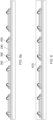
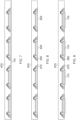
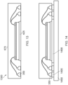
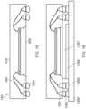
- the present disclosure relates to packaged semiconductors and to methods of making the same.
- it relates to so called lead-less packages such as ball grid array (BGA) packages, so called quad flat no lead (QFN) packages and similar packages.
- BGA ball grid array
- QFN quad flat no lead
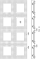
- lead frame which conventionally is electrically connected to the semiconductor die and provides means for electrical connection to the package.
- conventional lead frames may involve complex geometrical patterns, and, or in the alternative, may involve complex and delicate processing.
Landscapes
- Wire Bonding (AREA)
Applications Claiming Priority (1)
| Application Number | Priority Date | Filing Date | Title |
|---|---|---|---|
| CN202310670954.2A CN119108354A (zh) | 2023-06-07 | 2023-06-07 | 封装半导体装置及其制造方法 |
Publications (1)
| Publication Number | Publication Date |
|---|---|
| EP4475182A1 true EP4475182A1 (fr) | 2024-12-11 |
Family
ID=91247953
Family Applications (1)
| Application Number | Title | Priority Date | Filing Date |
|---|---|---|---|
| EP24177614.5A Pending EP4475182A1 (fr) | 2023-06-07 | 2024-05-23 | Dispositifs semi-conducteurs encapsulés et leurs procédés de fabrication |
Country Status (3)
| Country | Link |
|---|---|
| US (1) | US20240413065A1 (fr) |
| EP (1) | EP4475182A1 (fr) |
| CN (1) | CN119108354A (fr) |
Citations (3)
| Publication number | Priority date | Publication date | Assignee | Title |
|---|---|---|---|---|
| US20090042339A1 (en) * | 2007-08-10 | 2009-02-12 | Texas Instruments Incorporated | Packaged integrated circuits and methods to form a packaged integrated circuit |
| US9461009B1 (en) * | 2015-05-27 | 2016-10-04 | Freescale Semiconductor, Inc. | Method and apparatus for assembling a semiconductor package |
| US20200203263A1 (en) * | 2018-12-19 | 2020-06-25 | Texas Instruments Incorporated | Low cost reliable fan-out chip scale packages |
-
2023
- 2023-06-07 CN CN202310670954.2A patent/CN119108354A/zh active Pending
-
2024
- 2024-05-23 EP EP24177614.5A patent/EP4475182A1/fr active Pending
- 2024-06-04 US US18/732,697 patent/US20240413065A1/en active Pending
Patent Citations (3)
| Publication number | Priority date | Publication date | Assignee | Title |
|---|---|---|---|---|
| US20090042339A1 (en) * | 2007-08-10 | 2009-02-12 | Texas Instruments Incorporated | Packaged integrated circuits and methods to form a packaged integrated circuit |
| US9461009B1 (en) * | 2015-05-27 | 2016-10-04 | Freescale Semiconductor, Inc. | Method and apparatus for assembling a semiconductor package |
| US20200203263A1 (en) * | 2018-12-19 | 2020-06-25 | Texas Instruments Incorporated | Low cost reliable fan-out chip scale packages |
Also Published As
| Publication number | Publication date |
|---|---|
| US20240413065A1 (en) | 2024-12-12 |
| CN119108354A (zh) | 2024-12-10 |
Similar Documents
| Publication | Publication Date | Title |
|---|---|---|
| JP3062192B1 (ja) | リ―ドフレ―ムとそれを用いた樹脂封止型半導体装置の製造方法 | |
| US7799611B2 (en) | Partially patterned lead frames and methods of making and using the same in semiconductor packaging | |
| US7439097B2 (en) | Taped lead frames and methods of making and using the same in semiconductor packaging | |
| US7790500B2 (en) | Partially patterned lead frames and methods of making and using the same in semiconductor packaging | |
| US7622332B2 (en) | Partially patterned lead frames and methods of making and using the same in semiconductor packaging | |
| US6627977B1 (en) | Semiconductor package including isolated ring structure | |
| US9136247B2 (en) | Resin-encapsulated semiconductor device and method of manufacturing the same | |
| US6358778B1 (en) | Semiconductor package comprising lead frame with punched parts for terminals | |
| EP1237187A2 (fr) | Dispositif semi-conducteur encapsulé par une résine et son procédé de fabrication | |
| US20050218499A1 (en) | Method for manufacturing leadless semiconductor packages | |
| KR101286874B1 (ko) | 반도체 장치 및 그 제조 방법 | |
| JP3470111B2 (ja) | 樹脂封止型半導体装置の製造方法 | |
| JP3072291B1 (ja) | リ―ドフレ―ムとそれを用いた樹脂封止型半導体装置およびその製造方法 | |
| JP2003174131A (ja) | 樹脂封止型半導体装置及びその製造方法 | |
| CN101325190A (zh) | 导线架上具有图案的四方扁平无引脚封装结构 | |
| US20240413065A1 (en) | Packaged semiconductor devices and methods of making the same | |
| JPH10256460A (ja) | ターミナルランドフレームとそれを用いた樹脂封止型半導体装置およびその製造方法 | |
| JPH088385A (ja) | 樹脂封止型半導体装置 | |
| US20200321228A1 (en) | Method of manufacturing a lead frame, method of manufacturing an electronic apparatus, and electronic apparatus | |
| EP4579734A1 (fr) | Balle/bosse hybride et encapsulation de dispositif semi-conducteur à connexion par fil | |
| JP2001077285A (ja) | リードフレームとそれを用いた樹脂封止型半導体装置の製造方法 | |
| JP2001077275A (ja) | リードフレームとそれを用いた樹脂封止型半導体装置の製造方法 | |
| EP4535421A1 (fr) | Dispositif semi-conducteur encapsulé et son procédé de fabrication | |
| JP4362902B2 (ja) | 樹脂封止型半導体装置の製造方法 | |
| JP2001077136A (ja) | 樹脂封止型半導体装置の製造方法 |
Legal Events
| Date | Code | Title | Description |
|---|---|---|---|
| PUAI | Public reference made under article 153(3) epc to a published international application that has entered the european phase |
Free format text: ORIGINAL CODE: 0009012 |
|
| STAA | Information on the status of an ep patent application or granted ep patent |
Free format text: STATUS: THE APPLICATION HAS BEEN PUBLISHED |
|
| AK | Designated contracting states |
Kind code of ref document: A1 Designated state(s): AL AT BE BG CH CY CZ DE DK EE ES FI FR GB GR HR HU IE IS IT LI LT LU LV MC ME MK MT NL NO PL PT RO RS SE SI SK SM TR |
|
| STAA | Information on the status of an ep patent application or granted ep patent |
Free format text: STATUS: REQUEST FOR EXAMINATION WAS MADE |
|
| 17P | Request for examination filed |
Effective date: 20250611 |