EP4475414A1 - Procédé et programme informatique pour détecter un court-circuit dans un convertisseur de puissance, contrôleur pour commander un convertisseur de puissance et support lisible par ordinateur - Google Patents
Procédé et programme informatique pour détecter un court-circuit dans un convertisseur de puissance, contrôleur pour commander un convertisseur de puissance et support lisible par ordinateur Download PDFInfo
- Publication number
- EP4475414A1 EP4475414A1 EP23177505.7A EP23177505A EP4475414A1 EP 4475414 A1 EP4475414 A1 EP 4475414A1 EP 23177505 A EP23177505 A EP 23177505A EP 4475414 A1 EP4475414 A1 EP 4475414A1
- Authority
- EP
- European Patent Office
- Prior art keywords
- voltage
- inductance
- terminal
- power converter
- switch
- Prior art date
- Legal status (The legal status is an assumption and is not a legal conclusion. Google has not performed a legal analysis and makes no representation as to the accuracy of the status listed.)
- Pending
Links
Images
Classifications
-
- H—ELECTRICITY
- H02—GENERATION; CONVERSION OR DISTRIBUTION OF ELECTRIC POWER
- H02M—APPARATUS FOR CONVERSION BETWEEN AC AND AC, BETWEEN AC AND DC, OR BETWEEN DC AND DC, AND FOR USE WITH MAINS OR SIMILAR POWER SUPPLY SYSTEMS; CONVERSION OF DC OR AC INPUT POWER INTO SURGE OUTPUT POWER; CONTROL OR REGULATION THEREOF
- H02M1/00—Details of apparatus for conversion
- H02M1/32—Means for protecting converters other than automatic disconnection
-
- G—PHYSICS
- G01—MEASURING; TESTING
- G01R—MEASURING ELECTRIC VARIABLES; MEASURING MAGNETIC VARIABLES
- G01R31/00—Arrangements for testing electric properties; Arrangements for locating electric faults; Arrangements for electrical testing characterised by what is being tested not provided for elsewhere
- G01R31/40—Testing power supplies
- G01R31/42—AC power supplies
-
- G—PHYSICS
- G01—MEASURING; TESTING
- G01R—MEASURING ELECTRIC VARIABLES; MEASURING MAGNETIC VARIABLES
- G01R31/00—Arrangements for testing electric properties; Arrangements for locating electric faults; Arrangements for electrical testing characterised by what is being tested not provided for elsewhere
- G01R31/50—Testing of electric apparatus, lines, cables or components for short-circuits, continuity, leakage current or incorrect line connections
- G01R31/52—Testing for short-circuits, leakage current or ground faults
-
- H—ELECTRICITY
- H02—GENERATION; CONVERSION OR DISTRIBUTION OF ELECTRIC POWER
- H02M—APPARATUS FOR CONVERSION BETWEEN AC AND AC, BETWEEN AC AND DC, OR BETWEEN DC AND DC, AND FOR USE WITH MAINS OR SIMILAR POWER SUPPLY SYSTEMS; CONVERSION OF DC OR AC INPUT POWER INTO SURGE OUTPUT POWER; CONTROL OR REGULATION THEREOF
- H02M1/00—Details of apparatus for conversion
- H02M1/0003—Details of control, feedback or regulation circuits
- H02M1/0009—Devices or circuits for detecting current in a converter
-
- H—ELECTRICITY
- H02—GENERATION; CONVERSION OR DISTRIBUTION OF ELECTRIC POWER
- H02M—APPARATUS FOR CONVERSION BETWEEN AC AND AC, BETWEEN AC AND DC, OR BETWEEN DC AND DC, AND FOR USE WITH MAINS OR SIMILAR POWER SUPPLY SYSTEMS; CONVERSION OF DC OR AC INPUT POWER INTO SURGE OUTPUT POWER; CONTROL OR REGULATION THEREOF
- H02M1/00—Details of apparatus for conversion
- H02M1/32—Means for protecting converters other than automatic disconnection
- H02M1/34—Snubber circuits
- H02M1/348—Passive dissipative snubbers
-
- H—ELECTRICITY
- H02—GENERATION; CONVERSION OR DISTRIBUTION OF ELECTRIC POWER
- H02M—APPARATUS FOR CONVERSION BETWEEN AC AND AC, BETWEEN AC AND DC, OR BETWEEN DC AND DC, AND FOR USE WITH MAINS OR SIMILAR POWER SUPPLY SYSTEMS; CONVERSION OF DC OR AC INPUT POWER INTO SURGE OUTPUT POWER; CONTROL OR REGULATION THEREOF
- H02M7/00—Conversion of AC power input into DC power output; Conversion of DC power input into AC power output
- H02M7/42—Conversion of DC power input into AC power output without possibility of reversal
- H02M7/44—Conversion of DC power input into AC power output without possibility of reversal by static converters
- H02M7/48—Conversion of DC power input into AC power output without possibility of reversal by static converters using discharge tubes with control electrode or semiconductor devices with control electrode
- H02M7/483—Converters with outputs that each can have more than two voltages levels
- H02M7/487—Neutral point clamped inverters
-
- H—ELECTRICITY
- H02—GENERATION; CONVERSION OR DISTRIBUTION OF ELECTRIC POWER
- H02M—APPARATUS FOR CONVERSION BETWEEN AC AND AC, BETWEEN AC AND DC, OR BETWEEN DC AND DC, AND FOR USE WITH MAINS OR SIMILAR POWER SUPPLY SYSTEMS; CONVERSION OF DC OR AC INPUT POWER INTO SURGE OUTPUT POWER; CONTROL OR REGULATION THEREOF
- H02M7/00—Conversion of AC power input into DC power output; Conversion of DC power input into AC power output
- H02M7/42—Conversion of DC power input into AC power output without possibility of reversal
- H02M7/44—Conversion of DC power input into AC power output without possibility of reversal by static converters
- H02M7/48—Conversion of DC power input into AC power output without possibility of reversal by static converters using discharge tubes with control electrode or semiconductor devices with control electrode
- H02M7/53—Conversion of DC power input into AC power output without possibility of reversal by static converters using discharge tubes with control electrode or semiconductor devices with control electrode using devices of a triode or transistor type requiring continuous application of a control signal
- H02M7/537—Conversion of DC power input into AC power output without possibility of reversal by static converters using discharge tubes with control electrode or semiconductor devices with control electrode using devices of a triode or transistor type requiring continuous application of a control signal using semiconductor devices only, e.g. single switched pulse inverters
- H02M7/5387—Conversion of DC power input into AC power output without possibility of reversal by static converters using discharge tubes with control electrode or semiconductor devices with control electrode using devices of a triode or transistor type requiring continuous application of a control signal using semiconductor devices only, e.g. single switched pulse inverters in a bridge configuration
Definitions
- the invention relates to the field of power converters and more particularly to the field of Power Electronic Converters (PECs), e.g. for motor drives or wind converters.
- PECs Power Electronic Converters
- the invention relates to a method and a computer program for detecting a short-circuit in a power converter, to a controller for controlling the power converter, and to a computer-readable medium on which the computer program is stored.
- NPC Neutral Point Clamped
- the reliability of such converters is one of the challenges that need to be addressed, since medium-voltage multilevel converters have typically many semiconductor switches arranged in series and/or in parallel to increase either the voltage or, respectively, the current levels. By increasing the rated power of the converter, the number of power semiconductors may also be increased and thus, the reliability of the whole system may decrease. Any electrical fault, such as a short-circuit fault, may cause the malfunction of the whole medium-voltage system drive or even a catastrophic failure when the system does not include effective detection/protection functions. Therefore, the converter should be designed to have an effective fault-detecting method. Therefore, some modem PECs implement a protection concept to prevent hazards to persons and to minimize, respectively limit equipment damage in case of a fault.
- One important fault case is the short-circuit, where current starts to build up uncontrolled, e.g. because of a breakdown of an insulation (e.g. "flashover") or breakdown of a component of the converter (e.g. IGBT loss of blocking capability).
- a breakdown of an insulation e.g. "flashover”
- a component of the converter e.g. IGBT loss of blocking capability
- fault-tolerant solutions for power electronic systems For example, a detection and protection of the semiconductor devices via the corresponding gate drive, diagnostic solutions for medium-voltage drive systems with lower number of power semiconductor devices, and a larger number of fault-tolerant control strategies for medium voltage drives.
- the problem is that the available solutions are difficult to be implemented for medium-voltage drive application with a larger number of components.
- the common problems are either because too many sensors are used and the data is difficult to handle, or the measured data is too heavy to be transferred through the communication protocols and to be finally processed.
- An example of this problem is the detection of a power semiconductor short-circuit fault, which is typically based on the well-known desaturation protection circuit integrated in the gate driver.
- An on-state voltage of the semiconductor device is measured and compared to a defined threshold value to determine if a short-circuit fault exists.
- This solution is perfect when the aim is to protect a single device, but in the case of a medium-voltage NPC converter with several semiconductor devices in series/parallel, this solution has to be combined with another method to be able to detect and protect the drive in typically less than 10 ⁇ s, which may be a typical short-circuit withstanding time of such semiconductor devices (i.e., IGBTs and MOSFETs).
- IGBTs and MOSFETs i.e., IGBTs and MOSFETs
- an objective of the present invention is achieved by a method for detecting a short-circuit in a power converter.
- the power converter comprises a first DC terminal, a second DC terminal, an AC terminal, a first semiconductor switch electrically coupled to the first DC terminal and the AC terminal, a second semiconductor switch electrically coupled to the second DC terminal and the AC terminal, and an inductance.
- the method comprises: receiving a voltage signal which is representative for a switch voltage measured over the first semiconductor switch and the second semiconductor switch; determining an inductance voltage over the inductance depending on the measured switch voltage and a DC voltage between the first and second DC terminals; determining a current flowing through the semiconductor switches depending on the determined inductance voltage; and determining that the short-circuit is present depending on the determined current and a predetermined current threshold.
- the DC voltage may be known or measured in advance.
- the DC voltage may be fixed or variable.
- the DC voltage is unequal zero while the method is carried out. When the DC voltage is zero, the power converter does not operate and may be shut down.
- one of the semiconductor switches may be turned on and the other one may be turned off. For example, a turn-on signal may be sent to one of the semiconductor switches, e.g. to the first semiconductor switch, for turning on the corresponding semiconductor switch and a turn-off signal may be sent to the other one of the semiconductor switches, e.g. to the second semiconductor switch, for turning off the corresponding semiconductor switch.
- the power converter may comprise a DC link coupling the DC terminals to each other via a DC capacitor.
- One of the DC terminals may be a DC- terminal and the other one of the DC terminals may be a DC+ terminal.
- the semiconductor switches may be directly coupled to the AC terminal or via another converter stage of the power converter.
- the power converter may comprise a clamp circuit, e.g. a di/dt clamp circuit.
- the power converter may comprise one or more further semiconductor switches, DC links, clamp circuits, and/or a neutral point terminal, e.g. between two of the DC links.
- the power converter may be referred to as Power Electronic Converter (PEC).
- the power converter may be Neutral Point Clamped (NPC) converter, a half-bridge, a single phase of a two-level converter, a complete two-level converter, or a 3L-ANPC converter.
- NPC Neutral Point Clamped
- the first and/or second semiconductor switch each may be an Insulated-Gate Bipolar Transistor (IGBT). At least one of the semiconductor switches may be a high-power semiconductor switch and may be referred to as power semiconductor chip.
- IGBT Insulated-Gate Bipolar Transistor
- the inductance may be a parasitic inductance, e.g. comprising one or more electric lines of the power converter, and/or a dedicated inductance component, such as an inductor, e.g a di/dt limiting inductor, e.g. a coil.
- the inductance component may be omitted. This may contribute to a cost-efficiency, simplicity, and high reliability of the power converter.
- an inductance value of the inductance may be known in advance, e.g. by arranging the inductance component having the known inductance value and/or by measuring the parasitic inductance.
- the inductance component may be connected to a DC link capacitor of the DC link.
- the present disclosure provides an indirect method to detect the short-circuit by supervising the voltage that is applied on the inductance in the commutation path.
- This short-circuit detection method may be applicable to a broad range of PECs, not limited to a specific topology or semiconductor technology, scaling with voltage and current of the PEC, having low implementation effort basing on existing measurements and circuits present in a typical PEC and thus not compromising the overall reliability.
- short-circuit detection may be possible before the device enters the desaturation region, reducing the peak power and thus thermal stress on the device. Further, early detection of short-circuits allows turn-off sequences to be initiated at lower fault current levels compared to traditional DESAT detection methods, resulting overall in faster and more reliable fault containment.
- the voltage signal which is representative for the switch voltage, is representative for a first switch voltage and a second switch voltage. This enables to determine the contribution of the first and second semiconductor switches to the switch voltage.
- the voltage signal may be representative for a sum of the first and second switch voltages. The first and second switch voltages may be measured.
- the switch voltages are added together, the corresponding sum is subtracted from the DC voltage, and the difference is determined as the inductance voltage. This contributes to determine the inductance voltage over the inductance in an easy way.
- the difference when determining the current flowing through the semiconductor switches depending on the determined inductance voltage, the difference is integrated over the time and the corresponding integral is determined as the current. For example, the voltage-time-area over the inductance may be integrated.
- the integration enables to calculate a short-circuit current.
- the difference or the integral When integrating the difference over the time, the difference or the integral may be divided by the inductance value, if the inductance value is constant. Otherwise, in case of the inductance value not being constant, the difference may be divided by the inductance value and this quotient may be integrated, wherein the corresponding integral may be the short-circuit current.
- the short-circuit when determining that the short-circuit is present depending on the determined current and the predetermined current threshold, the short-circuit is determined as being present when the determined current reaches or exceeds the predetermined current threshold.
- the predetermined current threshold may be predetermined by a manufacturer of the power converter.
- the predetermined current threshold may be that current until which the semiconductor switches are not damaged, at least for a short period of time.
- a reference DC voltage signal is sent to an energy source coupled to the DC terminals, wherein the energy source provides the DC voltage to the DC terminals upon receiving the reference DC voltage signal.
- the reference DC voltage signal may be representative for the DC voltage and the DC voltage may be referred to as reference DC voltage or DC voltage reference.
- a second DC voltage signal is received before determining the inductance voltage, wherein the second DC voltage signal is representative for the DC voltage and wherein the second DC voltage signal is determined from a voltage measurement.
- the DC voltage may be measured directly, e.g. at the DC link, or the switch voltages may be measured and the DC voltage may be derived from the measured switch voltages.
- a mean value of the inductance voltage can be assumed to be zero. Therefore, a mean value or low pass filtered value of the sum of the switch voltages may correspond to the DC-voltage. So, if it is not the case already, the power converter should be supplied with energy in form of the DC voltage before carrying out the above method.
- the at least parasitic inductance is an inductance component of the power converter.
- the inductance component may be an inductor, e.g. a di/dt limiting inductor, e.g. a coil.
- the inductance component may be arranged in the commutation path of the power converter, e.g. between one of the semiconductor switches, e.g. the first semiconductor switch, and the DC-terminal to which the corresponding semiconductor switch is coupled.
- the inductance component may be a part of the clamp circuit.
- the power converter may correspond to the above power converter.
- the power converter again comprises the first DC terminal, the second DC terminal, the AC terminal, the first semiconductor switch electrically coupled to the first DC terminal and the AC terminal, the second semiconductor switch electrically coupled to the second DC terminal and the AC terminal, and the inductance.
- the method comprises: receiving a voltage signal which is representative for the switch voltage measured over the first semiconductor switch and the second semiconductor switch; determining whether the switch voltage does not exceed a given forward voltage of the semiconductor switches; when the switch voltage does not exceed the given forward voltage, determining a duration during which the switch voltage does not exceed the given forward voltage; and determining that the short-circuit is present when the determined duration reaches or exceeds a duration threshold.
- the given forward voltage may be a normal and/or specific forward voltage of the semiconductor switches.
- Determining the duration and determining that the short-circuit is present when the determined duration reaches or exceeds a duration threshold is based on the insight of the inventors that when neither the first semiconductor switch nor the second semiconductor switch see any voltage it can be concluded that the DC voltage is applied over the inductance.
- the current through the semiconductor switches is proportional to the DC voltage and the duration during which the voltage is present, and inverse proportional to the inductance value of the inductance.
- the duration threshold may be easily determined depending on the predetermined current threshold, and it is sufficient to measure the duration only and to compare it with the duration threshold.
- the method according to the second aspect comprises the step of determining the inductance voltage over the parasitic inductance depending on the measured switch voltage and the DC voltage by recognizing that the switch voltage does not exceed the given forward voltage of the semiconductor switches and by setting the inductance voltage as the DC voltage.
- the duration is representative for the current, because the duration is proportional to the current and because the proportionality factor, i.e. the inductance value divided by the DC voltage, is known. So, both aspects are based on the same inventive idea, and the steps of the corresponding methods are the same or at least similar, wherein the method according to the second aspect may be even faster, simpler, more cost-efficient, and/or more reliable than the method according to the first aspect.
- the above advantages and/or effects of the method according to the first aspect may be transferred to the method according to the second aspect. Therefore, a repetition of these advantages and/or effects is omitted and it is referred to the above explanations only in order to provide a concise description.
- the physical features of the power converter according to the first aspect may be transferred to physical features of the power converter according to the second aspect. In other words, the above two methods may be carried out at the same power converter.
- the duration threshold is determined by multiplying an inductance value of the inductance with a predetermined maximum fault current and by dividing the corresponding product by a DC voltage between the first and second DC terminals.
- the predetermined maximal fault current may correspond to the above current threshold.
- the reference DC voltage signal is sent to the energy source coupled to the DC terminals, wherein the energy source provides the DC voltage to the DC terminals upon receiving the reference DC voltage signal.
- the reference DC voltage signal may be representative for the DC voltage and the DC voltage may be referred to as reference DC voltage or DC voltage reference.
- the second DC voltage signal is received before determining the duration threshold, wherein the second DC voltage signal is representative for the DC voltage and wherein the second DC voltage signal is determined from the voltage measurement.
- the DC voltage may be measured directly, e.g. at the DC link, or the switch voltages may be measured and the DC voltage may be derived from the measured switch voltages.
- a mean value of the inductance voltage can be assumed to be zero. Therefore, a mean value or low pass filtered value of the sum of the switch voltages may correspond to the DC-voltage.
- the inductance is the inductance component of the power converter.
- the controller comprises: an input terminal for receiving one or more of the voltage signals; an output terminal for sending one or more control signals to the power converter; and a processor configured for carrying out at least one of the above methods.
- An objective is achieved by a computer program for detecting the short-circuit in the power converter.
- the computer program when being carried out by the processor of the controller for controlling the power converter, carrying out at least one of the above methods.
- An objective is achieved by a computer-readable medium on which the computer program is stored.
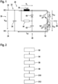
- Fig. 1 schematically shows a circuit diagram of an exemplary embodiment of a power converter 20.
- the power converter 20 may be a Power Electronic Converter (PEC).
- the power converter 20 may be a part of a Neutral Point Clamped (NPC) converter, a half-bridge, a single phase of a two-level converter, a part of a complete two-level converter, or a part of a 3L-ANPC converter.
- the power converter 20 may be used in an inverter or rectifier.
- the power converter 20 may be implemented as or for a medium-voltage drive application.
- the power converter 20 comprises a first DC terminal 22, e.g. a DC+ terminal, a second DC terminal 24, e.g. a DC- terminal, an output, e.g. provided by an AC terminal 26, a first semiconductor switch S1 electrically coupled to the first DC terminal 22 and the AC terminal 26, a second semiconductor switch S2 electrically coupled to the second DC terminal 24 and the AC terminal 26, and an inductance.
- the DC terminals 22, 24 are coupled to an energy source 30, in particular a DC energy source, e.g. a battery, a rectifier, e.g. an active rectifier, a solar panel, a DC grid, etc.
- the semiconductor switches S1, S2 may be directly coupled to the AC terminal 26 or via another converter stage (not shown) of the power converter 20, e.g. in case of a three-level NPC or ANPC converter.
- the first and/or second semiconductor switches S1, S2 each may be an Insulated-Gate Bipolar Transistor (IGBT).
- IGBT Insulated-Gate Bipolar Transistor
- At least one of the semiconductor switches S1, S2 may be a high-power semiconductor switch and may be referred to as power semiconductor switch.
- the power converter 20 may further comprise a DC link 32 coupling the DC terminals 22, 24 to each other, e.g. via a first capacitor 34, in other words a DC capacitor.
- the power converter 20 may further comprise a clamp circuit 40, e.g. a di/dt clamp circuit.
- the clamp circuit 40 may comprise a second capacitor 42 and a diode 46 electrically arranged in series and electrically coupling the DC terminals 22, 24 to each other.
- the clamp circuit 40 may further comprise a resistor 44 coupling a node between the second capacitor 42 and the diode 46 to the first DC terminal 22.
- the inductance may be a parasitic inductance, e.g. comprising one or more electric lines of the power converter, and/or an inductance component 36, such as an inductor, e.g. a di/dt limiting inductor, e.g. a coil. In the former case, the inductance component 36 may be omitted.
- the inductance component 36 may be connected to the first capacitor 34 of the DC link 32.
- the inductance component 36 may be arranged between to nodes at which the clamp circuit 40 is electrically coupled to the first DC terminal 22.
- the one or more electric lines forming the parasitic inductance may be a part of a commutation path of the power converter 20.
- the commutation path may extend from one of the DC terminals 22, 24 via the semiconductor switches S1, S2 to the other one of the DC terminals 22, 24.
- an inductance value of the inductance may be known in advance, e.g. by arranging the inductance component 36 having the known inductance value and/or by measuring the parasitic inductance in at least a part of the commutation path.
- the power converter 20 may comprise one or more further semiconductor switches, DC links, clamp circuits, and/or a neutral point terminals, e.g. between two of the corresponding further DC links.
- a short-circuit 18 may be present in the power converter 20.
- the short-circuit 18 may bypass one of the semiconductor switches S1, S2, e.g. the second semiconductor switch S2.
- the output of the power converter 20, which is the AC terminal 26 in this embodiment may be directly coupled with the second DC terminal 24. If the first semiconductor S1 is turned on and as such electrically conductive, the first and second DC terminals 22, 24 are short-circuited by the turned-on first semiconductor switch S1 and the short-circuit 18.
- the proposed methods are generic in nature and can be applied to multi-level topologies like for example the 3L-ANPC.
- the topology of the 3L-ANPC may be easily derived from the power converter shown in figure 1 .
- the power converter 20 may be duplicated wherein the double may be arranged below the power converter 20, e.g. such that the commutation path from the second semiconductor switch S2 to the second DC terminal 24 is shared between the power converter 20 and the double, wherein this shared part of the commutation path forms the neutral point potential of the 3L-ANPC.
- the outputs of the power converter 20 and the double may be coupled to each other via two further semiconductor switches, wherein a node between the two further semiconductor chips may provide an AC terminal and as such an output of the 3L-ANPC.
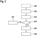
- Fig. 2 schematically shows a flow-chart of an exemplary embodiment of a method for detecting a short-circuit in a power converter, e.g. the short-circuit 18 in the above power converter 20.
- the method may be carried out when energy is supplied to the power converter 20 by the energy source 30. So, the method may be carried out when a DC voltage V DC between the DC terminals 22, 24 is unequal zero.
- the method may be carried out by a controller configured for controlling the power converter 20.
- the controller may be a part of the power converter 20 or may be external with respect to the power converter 20.
- a reference DC voltage signal may be sent to the energy source 30 coupled to the DC terminals 22, 24.
- the reference DC voltage signal may be representative for the DC voltage V DC and the DC voltage V DC may be referred to as reference DC voltage or DC voltage reference.
- the energy source 30 may provide the DC voltage V DC to the DC terminals 22, 24 upon receiving the reference DC voltage signal.
- a second DC voltage signal may be received before determining an inductance voltage V L over the above explained inductance, i.e.
- the second DC voltage signal may be representative for the DC voltage V DC and wherein the DC voltage may be derived from the measured switch voltages.
- the second voltage signal may be generated by a voltmeter and may be received by the controller (not shown) for controlling the power converter 20.
- a turn-on signal ON may be sent to the first semiconductor switch S 1 for turning on the first semiconductor switch S 1 and a turn-off signal OFF may be sent to the second semiconductor switch S2 for turning off the second semiconductor switch S2.
- the short-circuit 18 short-circuits the DC terminals 22, 24 with each other.
- a voltage signal which is representative for a switch voltage v S1 , v S2 measured over the first semiconductor switch S 1 and the second semiconductor switch S2 may be measured.
- the voltage signal, which is representative for the switch voltage v S1 , v S2 may be representative for a first switch voltage vsi over the first semiconductor switch S 1 and a second switch voltage v S2 over the second semiconductor switch S2.
- the inductance voltage V L over the inductance may be determined depending on the measured switch voltage(s) v S1 , v S2 and the DC voltage V DC between the first and second DC terminals 22, 24.
- a current isc in particular a short-circuit current, flowing through the semiconductor switches S1, S2 may be determined depending on the determined inductance voltage V L .
- a step S12 it may be determined that the short-circuit 18 is present depending on a predetermined current threshold i SC_max being the maximal acceptable fault current, as shown below.
- the short-circuit 18 may be determined as being present when the current isc determined in step S10 reaches or exceeds the predetermined current threshold i SC_max .
- a predetermined fault reaction e.g. a predetermined turn-off sequence, may be executed.
- Fig. 3 schematically shows a flow-chart of another exemplary embodiment of a method for detecting a short-circuit in a power converter, e.g. the short-circuit 18 of the above power converter 20.
- the method may be carried out when energy is supplied to the power converter 20 by the energy source 30. So, the method may be carried out when the DC voltage V DC between the DC terminals 22, 24 is unequal zero.
- the method may be carried out by a controller configured for controlling the power converter 20.
- the controller may be a part of the power converter 20 or may be external with respect to the power converter 20.
- An optional step S20 may correspond to the optional step S2 explained above.
- An optional step S22 may correspond to the optional step S4 explained above.
- a voltage signal which is representative for the switch voltages v S1 , v S2 over the first semiconductor switch S1 and the second semiconductor switch S2 may be received.
- step S25 it may be determined, whether the switch voltages v S1 , v S2 do not exceed a given forward voltage of the semiconductor switches S1, S2. If the condition of step S25 is fulfilled, the method proceeds in a step S26. If the condition of step S25 is not fulfilled, the method proceeds in a step S27.
- step S26 a duration during which the switch voltage v S1 , v S2 do not exceed the given forward voltage may be determined.
- step S27 the method may be terminated and/or it may be determined that no short-circuit is present.
- a step S28 it may be determined that the short-circuit 18 is present when the determined duration reaches or exceeds a duration threshold.
- the predetermined fault reaction e.g. a predetermined turn-off sequence, may be executed.
Landscapes
- Engineering & Computer Science (AREA)
- Power Engineering (AREA)
- Physics & Mathematics (AREA)
- General Physics & Mathematics (AREA)
- Inverter Devices (AREA)
- Power Conversion In General (AREA)
Priority Applications (3)
| Application Number | Priority Date | Filing Date | Title |
|---|---|---|---|
| EP23177505.7A EP4475414A1 (fr) | 2023-06-06 | 2023-06-06 | Procédé et programme informatique pour détecter un court-circuit dans un convertisseur de puissance, contrôleur pour commander un convertisseur de puissance et support lisible par ordinateur |
| PCT/EP2024/061839 WO2024251438A1 (fr) | 2023-06-06 | 2024-04-30 | Procédé et programme informatique pour détection d'un court-circuit dans un convertisseur de puissance, dispositif de commande pour la commande d'un convertisseur de puissance et support lisible par ordinateur |
| CN202480037637.XA CN121263951A (zh) | 2023-06-06 | 2024-04-30 | 用于检测功率转换器中的短路的方法和计算机程序,用于控制功率转换器的控制器以及计算机可读介质 |
Applications Claiming Priority (1)
| Application Number | Priority Date | Filing Date | Title |
|---|---|---|---|
| EP23177505.7A EP4475414A1 (fr) | 2023-06-06 | 2023-06-06 | Procédé et programme informatique pour détecter un court-circuit dans un convertisseur de puissance, contrôleur pour commander un convertisseur de puissance et support lisible par ordinateur |
Publications (1)
| Publication Number | Publication Date |
|---|---|
| EP4475414A1 true EP4475414A1 (fr) | 2024-12-11 |
Family
ID=86692631
Family Applications (1)
| Application Number | Title | Priority Date | Filing Date |
|---|---|---|---|
| EP23177505.7A Pending EP4475414A1 (fr) | 2023-06-06 | 2023-06-06 | Procédé et programme informatique pour détecter un court-circuit dans un convertisseur de puissance, contrôleur pour commander un convertisseur de puissance et support lisible par ordinateur |
Country Status (3)
| Country | Link |
|---|---|
| EP (1) | EP4475414A1 (fr) |
| CN (1) | CN121263951A (fr) |
| WO (1) | WO2024251438A1 (fr) |
Citations (6)
| Publication number | Priority date | Publication date | Assignee | Title |
|---|---|---|---|---|
| US6304472B1 (en) * | 1999-05-14 | 2001-10-16 | Hitachi, Ltd. | Electric power converting system with integrator providing output indicative of current |
| US20090251831A1 (en) * | 2006-06-30 | 2009-10-08 | Toyota Jidosha Kabushiki Kaisha | Motor drive device |
| US20120206841A1 (en) * | 2011-02-10 | 2012-08-16 | General Electric Company | Power converter and method of operation |
| US8872455B2 (en) * | 2012-05-22 | 2014-10-28 | Deere & Company | Method and controller for an electric motor with fault detection |
| EP2747260B1 (fr) * | 2012-12-21 | 2019-08-14 | GE Energy Power Conversion GmbH | Procédé pour faire fonctionner un redresseur de puissance électrique et redresseur de puissance électrique |
| WO2020120312A1 (fr) * | 2018-12-13 | 2020-06-18 | Robert Bosch Gmbh | Décharge d'un condensateur de circuit intermédiaire d'un onduleur au moyen d'impulsions de court-circuit de pont |
-
2023
- 2023-06-06 EP EP23177505.7A patent/EP4475414A1/fr active Pending
-
2024
- 2024-04-30 WO PCT/EP2024/061839 patent/WO2024251438A1/fr not_active Ceased
- 2024-04-30 CN CN202480037637.XA patent/CN121263951A/zh active Pending
Patent Citations (6)
| Publication number | Priority date | Publication date | Assignee | Title |
|---|---|---|---|---|
| US6304472B1 (en) * | 1999-05-14 | 2001-10-16 | Hitachi, Ltd. | Electric power converting system with integrator providing output indicative of current |
| US20090251831A1 (en) * | 2006-06-30 | 2009-10-08 | Toyota Jidosha Kabushiki Kaisha | Motor drive device |
| US20120206841A1 (en) * | 2011-02-10 | 2012-08-16 | General Electric Company | Power converter and method of operation |
| US8872455B2 (en) * | 2012-05-22 | 2014-10-28 | Deere & Company | Method and controller for an electric motor with fault detection |
| EP2747260B1 (fr) * | 2012-12-21 | 2019-08-14 | GE Energy Power Conversion GmbH | Procédé pour faire fonctionner un redresseur de puissance électrique et redresseur de puissance électrique |
| WO2020120312A1 (fr) * | 2018-12-13 | 2020-06-18 | Robert Bosch Gmbh | Décharge d'un condensateur de circuit intermédiaire d'un onduleur au moyen d'impulsions de court-circuit de pont |
Also Published As
| Publication number | Publication date |
|---|---|
| WO2024251438A1 (fr) | 2024-12-12 |
| CN121263951A (zh) | 2026-01-02 |
Similar Documents
| Publication | Publication Date | Title |
|---|---|---|
| KR102849055B1 (ko) | 게이트 드라이버 회로용 단락 검출 및 보호와 로직 분석을 사용하여 이를 검출하는 방법 | |
| Wang et al. | A submodule fault ride-through strategy for modular multilevel converters with nearest level modulation | |
| JP4538047B2 (ja) | 電力用素子の故障検出装置 | |
| US11119159B2 (en) | On-line diagnostic method for electronic switch faults in neutral-point-clamped converters | |
| AU2005258128B2 (en) | Inverter bridge controller implementing short-circuit protection scheme | |
| Zhang et al. | Open-circuit fault diagnosis for cascaded H-bridge multilevel inverter based on LS-PWM technique | |
| JP2009506736A (ja) | 分散配置されたエネルギー蓄積器を有する電力変換回路 | |
| US9712044B2 (en) | Power converter | |
| JP4930866B2 (ja) | 電力用素子の故障検出装置 | |
| CN108141132B (zh) | 多相转换器 | |
| EP4148964A1 (fr) | Procédé et dispositif pour compenser un commutateur défectueux dans un convertisseur à condensateur flottant à plusieurs niveaux | |
| US7583109B2 (en) | Apparatus and methods for monitoring parallel-connected power switching devices responsive to drive circuit parameters | |
| Anand et al. | Open switch fault detection in Cascaded H-Bridge Multilevel Inverter using normalised mean voltages | |
| Ali et al. | Ride through strategy for a three-level dual Z-source inverter using TRIAC | |
| US12301130B2 (en) | Power conversion device and method of diagnosing failures of switching devices | |
| CA2855496C (fr) | Procede d'elimination d'un arc electrique genere par au moins une source de tension simple d'un circuit onduleur | |
| EP4475414A1 (fr) | Procédé et programme informatique pour détecter un court-circuit dans un convertisseur de puissance, contrôleur pour commander un convertisseur de puissance et support lisible par ordinateur | |
| JPH10164854A (ja) | 電力変換器 | |
| CN108684213B (zh) | 半导体模块、在半导体模块中使用的开关元件的选定方法以及开关元件的芯片设计方法 | |
| US12362682B2 (en) | Frequency converter with ground fault detection | |
| CN117955063A (zh) | 光伏系统及其控制方法 | |
| JP7322653B2 (ja) | スイッチの駆動装置 | |
| Pallo et al. | Short-circuit fault ride-through of flying-capacitor multilevel converters through rapid fault detection and idle-mode operation | |
| EP4660644A1 (fr) | Procédé de détection de l'état d'une première unité de commutation d'un système d'alimentation et système d'alimentation | |
| Kutrolli et al. | Model-based Fault Diagnostics in Cascaded H-Bridge Inverters with Level-shifted Modulation |
Legal Events
| Date | Code | Title | Description |
|---|---|---|---|
| PUAI | Public reference made under article 153(3) epc to a published international application that has entered the european phase |
Free format text: ORIGINAL CODE: 0009012 |
|
| STAA | Information on the status of an ep patent application or granted ep patent |
Free format text: STATUS: THE APPLICATION HAS BEEN PUBLISHED |
|
| AK | Designated contracting states |
Kind code of ref document: A1 Designated state(s): AL AT BE BG CH CY CZ DE DK EE ES FI FR GB GR HR HU IE IS IT LI LT LU LV MC ME MK MT NL NO PL PT RO RS SE SI SK SM TR |
|
| STAA | Information on the status of an ep patent application or granted ep patent |
Free format text: STATUS: REQUEST FOR EXAMINATION WAS MADE |
|
| 17P | Request for examination filed |
Effective date: 20250318 |
|
| STAA | Information on the status of an ep patent application or granted ep patent |
Free format text: STATUS: EXAMINATION IS IN PROGRESS |
|
| 17Q | First examination report despatched |
Effective date: 20250801 |