EP4475494A2 - Procédé et dispositif de commande de composants électriques et/ou électroniques d'un module de véhicule automobile - Google Patents
Procédé et dispositif de commande de composants électriques et/ou électroniques d'un module de véhicule automobile Download PDFInfo
- Publication number
- EP4475494A2 EP4475494A2 EP24207813.7A EP24207813A EP4475494A2 EP 4475494 A2 EP4475494 A2 EP 4475494A2 EP 24207813 A EP24207813 A EP 24207813A EP 4475494 A2 EP4475494 A2 EP 4475494A2
- Authority
- EP
- European Patent Office
- Prior art keywords
- bus
- bus node
- addressing
- node
- der
- Prior art date
- Legal status (The legal status is an assumption and is not a legal conclusion. Google has not performed a legal analysis and makes no representation as to the accuracy of the status listed.)
- Pending
Links
Images







Classifications
-
- H—ELECTRICITY
- H04—ELECTRIC COMMUNICATION TECHNIQUE
- H04L—TRANSMISSION OF DIGITAL INFORMATION, e.g. TELEGRAPHIC COMMUNICATION
- H04L12/00—Data switching networks
- H04L12/28—Data switching networks characterised by path configuration, e.g. LAN [Local Area Networks] or WAN [Wide Area Networks]
- H04L12/40—Bus networks
- H04L12/40006—Architecture of a communication node
- H04L12/40045—Details regarding the feeding of energy to the node from the bus
-
- H—ELECTRICITY
- H04—ELECTRIC COMMUNICATION TECHNIQUE
- H04L—TRANSMISSION OF DIGITAL INFORMATION, e.g. TELEGRAPHIC COMMUNICATION
- H04L12/00—Data switching networks
- H04L12/28—Data switching networks characterised by path configuration, e.g. LAN [Local Area Networks] or WAN [Wide Area Networks]
- H04L12/40—Bus networks
- H04L12/403—Bus networks with centralised control, e.g. polling
-
- H—ELECTRICITY
- H04—ELECTRIC COMMUNICATION TECHNIQUE
- H04L—TRANSMISSION OF DIGITAL INFORMATION, e.g. TELEGRAPHIC COMMUNICATION
- H04L12/00—Data switching networks
- H04L12/28—Data switching networks characterised by path configuration, e.g. LAN [Local Area Networks] or WAN [Wide Area Networks]
- H04L12/40—Bus networks
- H04L12/4013—Management of data rate on the bus
-
- H—ELECTRICITY
- H04—ELECTRIC COMMUNICATION TECHNIQUE
- H04L—TRANSMISSION OF DIGITAL INFORMATION, e.g. TELEGRAPHIC COMMUNICATION
- H04L12/00—Data switching networks
- H04L12/28—Data switching networks characterised by path configuration, e.g. LAN [Local Area Networks] or WAN [Wide Area Networks]
- H04L12/40—Bus networks
- H04L12/40169—Flexible bus arrangements
- H04L12/40176—Flexible bus arrangements involving redundancy
- H04L12/40182—Flexible bus arrangements involving redundancy by using a plurality of communication lines
-
- H—ELECTRICITY
- H04—ELECTRIC COMMUNICATION TECHNIQUE
- H04L—TRANSMISSION OF DIGITAL INFORMATION, e.g. TELEGRAPHIC COMMUNICATION
- H04L61/00—Network arrangements, protocols or services for addressing or naming
- H04L61/50—Address allocation
- H04L61/5038—Address allocation for local use, e.g. in LAN or USB networks, or in a controller area network [CAN]
-
- H—ELECTRICITY
- H05—ELECTRIC TECHNIQUES NOT OTHERWISE PROVIDED FOR
- H05B—ELECTRIC HEATING; ELECTRIC LIGHT SOURCES NOT OTHERWISE PROVIDED FOR; CIRCUIT ARRANGEMENTS FOR ELECTRIC LIGHT SOURCES, IN GENERAL
- H05B47/00—Circuit arrangements for operating light sources in general, i.e. where the type of light source is not relevant
- H05B47/10—Controlling the light source
- H05B47/175—Controlling the light source by remote control
- H05B47/18—Controlling the light source by remote control via data-bus transmission
-
- H—ELECTRICITY
- H05—ELECTRIC TECHNIQUES NOT OTHERWISE PROVIDED FOR
- H05B—ELECTRIC HEATING; ELECTRIC LIGHT SOURCES NOT OTHERWISE PROVIDED FOR; CIRCUIT ARRANGEMENTS FOR ELECTRIC LIGHT SOURCES, IN GENERAL
- H05B47/00—Circuit arrangements for operating light sources in general, i.e. where the type of light source is not relevant
- H05B47/10—Controlling the light source
- H05B47/175—Controlling the light source by remote control
- H05B47/198—Grouping of control procedures or address assignation to light sources
-
- H—ELECTRICITY
- H04—ELECTRIC COMMUNICATION TECHNIQUE
- H04L—TRANSMISSION OF DIGITAL INFORMATION, e.g. TELEGRAPHIC COMMUNICATION
- H04L12/00—Data switching networks
- H04L12/28—Data switching networks characterised by path configuration, e.g. LAN [Local Area Networks] or WAN [Wide Area Networks]
- H04L12/40—Bus networks
- H04L2012/40267—Bus for use in transportation systems
- H04L2012/40273—Bus for use in transportation systems the transportation system being a vehicle
Definitions
- the present patent application takes the priorities of the German patent applications 10 2018 104 847.5 of 2 March 2018 , 10 2018 104 850.5 of 2 March 2018 , 10 2018 104 852.1 of 2 March 2018 , 10 2018 104 855.6 of 2 March 2018 , 10 2018 104 858.0 of March 2, 2018 , 10 2018 104 862.9 of 2 March 2018 , 10 2018 104 864.5 of 2 March 2018 , 10 2018 104 865.3 of 2 March 2018 , 10 2018 104 866.1 of 2 March 2018 , 10 2018 104 868.8 of 2 March 2018 and 10 2018 104 871.8 of 2 March 2018 the contents of which are hereby incorporated by reference into the subject matter of the present patent application.
- the invention relates to methods and devices for controlling electrical and/or electronic components of a motor vehicle module, in particular an interior light and/or exterior light such as a rear light module of a motor vehicle. Furthermore, the invention relates to a motor vehicle module with several electrical and/or electronic components, in particular an interior light and/or exterior light such as a rear light module of a motor vehicle.
- the multitude of components of a motor vehicle module for example the multitude of LEDs or OLEDs assigned to the individual light functions of a rear light module, are advantageously connected to a control unit of the module via a communication bus or are in communication with the control unit via the communication bus.
- the The control unit also includes a voltage converter to supply the LED drivers of a light module.
- Differential two-wire communication bus systems have proven themselves in terms of transmission speed and robustness.
- the information signals are transmitted between the control unit and the participants as a voltage difference between the two bus lines, which results in greater signal reliability and a higher transmission speed and a lower susceptibility to interference.
- Two-wire bus lines of this type are generally known.
- the problem is that the hardware effort for such two-wire bus systems and their participants is not insignificant.
- a disadvantage, particularly in terms of costs, is the fact that the participants must have relatively precise clock generators that work synchronously with each other.
- the light modules must be able to determine their physical position when installed and connected in the vehicle factory and convert it into a logical address so that similar light modules can be used without pre-programming a bus node address for these light modules, which massively reduces the possibility of errors and logistics in production.
- a device for controlling an adaptive automotive headlight with an FPGA-based LIN controller is described in GUO JINYAN ET AL: "The design and realization of CAN bit timing logic", MICROELECTRONICS AND ELECTRONIS (PRIMEASIA), 2010 ASIA PACIFIC CONFERENCE ON POSTGRADUATE RESEARCH IN, IEEE, PISCATAWAY, NJ, USA, 22. September 2010 (2010-09-22), pages 333-337, XP031777603, ISBN: 978-1-4244-6735-8 described.
- the object of the invention is to provide a device for controlling electrical and/or electronic components of a motor vehicle module and such a motor vehicle module which is reduced in terms of hardware expenditure.
- the indices j and n each correspond to a positive integer.
- the proposed approach combines the advantages of a differential two-wire communication bus with auto-addressing capability with the advantages of using asynchronous, digital, serial interfaces, via which the individual participants or the individual components are connected to the two-wire communication bus.
- UART Universal Asynchronous Receiver Transmitters
- Such synchronization information e.g. synchronization bits
- the protocol of the differential two-wire communication bus used according to the invention thus includes elements such as For example, these are known from single-wire buses whose participants have standardized and cost-effective UARTs.
- the invention can be used in particular in the context of digital interfaces for robust and high-speed transmission of data via a two-wire cable connection between boards equipped with LEDs, for example for rear lights and interior lights within a lamp, with a data rate of up to 500 kbit/s.
- the symmetrical transmission is used by means of a differential high-speed two-wire bus system for the purpose of transmitting a simple serial protocol and thus reducing the digital hardware effort.
- a serial, bidirectional differential two-wire communication bus is operated, in simple terms, according to a serial, bidirectional one-wire communication bus.
- One of the essential features of the invention is to achieve the phase and frequency synchronization of the sampling signal generated in each bus node by transmitting corresponding bits.
- both phase and frequency synchronization takes place in this way.
- the bus nodes operated in this way expediently have typical UARTS (Universal Asynchronous Receiver Transmitter).
- frequency synchronization in the true sense can also be implemented in another way if it is assumed that each bus node samples the bits transmitted over the two-wire communication bus by means of oversampling. Then it is possible to ensure frequency synchronization by adapting the oversampling of the bits transmitted over the two-wire communication bus, which is typically used in the bus node, by selecting the sampling point(s) per bit that are used to decide on the logical state of the bit, over the bits of one or more bit words, at different times, so that without frequency synchronization of the clock of the bus node to the clock of the bus master, these sampling points are used for the duration of of reading a bit word or several bit words is always essentially in the middle of a bit.
- a bus shunt resistor is sometimes mentioned as an example of a current measuring device. It should be emphasized at this point that the bus shunt resistor is not the only way of implementing a current measuring device. For example, other current measuring methods known to those skilled in the art can also be used.
- the invention proposes further devices and methods which are the subject matter of the respective independent patent claims 1, 2, 4, 14, 15, 24, 26, 28, 29, 33, 47, 60 and 75.
- Individual embodiments of the respective methods and devices of the aforementioned claims are the subject matter of the respective subclaims relating to these patent claims.
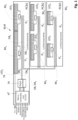
- the Figure 1 shows an example of a tail light module (BLM) of a motor vehicle.
- the tail light module (BLM) has a bus master (ECU) and a serial, bidirectional, differential two-wire communication bus (DB).
- the serial, bidirectional and differential two-wire communication bus (DB) consists of a first single-wire bus (DB a ) and a second single-wire bus (DB b ).
- the TXD and RXD lines of the bus master (ECU) lead to a level converter (TR) to convert the signal level for the operation of the two-wire communication bus DB.
- the bus master (ECU) receives various control commands from outside, for example for the functions tail light, indicator, rear fog light, dynamic effects, etc., and/or information via a digital bus.
- the bus master converts these commands into bit streams, which, among other things, have bits of a synchronization field of the corresponding data frames (bit stream packet (BP)).
- Level converter and bus master are also considered as a unit in the following and are referred to jointly as bus master (ECU).
- bus nodes BK 1 to BK 6 Various components or participants are connected to the communication bus (DB) as bus nodes BK 1 to BK 6.
- the first and second bus nodes ((BK 1 ) and (BK 2 )) are responsible for implementing the flashing light
- the third bus node (BK 3 ) for implementing the tail light
- the fourth and sixth bus nodes (BK 4 ) and (BK 6 ) for executing the brake light function
- the fifth bus node (BK 5 ) for implementing the reversing light.
- Each of these participants or components has a large number of LEDs (LED 1 to LED 6 ) that are controlled by the respective LED drivers.
- Each bus node is also provided with a digital interface (IF 1 to IF 6 ) in the form of a UART. Furthermore, each bus node has a microcontroller ([ ⁇ C 1 ] to [ ⁇ C 6 ]) and a clock generator ([CLKG 1 ] to [CLKG 6 ]) if required in order to be able to read messages on the differential two-wire communication bus (DB) synchronously with the transmission of the bits of the bit streams or to be able to place such bit streams on the two-wire communication bus (DB) synchronously for reading by other participants or the bus master (ECU).
- DB differential two-wire communication bus
- ECU bus master
- the simplification of the hardware for controlling the components of a motor vehicle module according to the invention is also helped by working with fixed sampling points at the level of the components or two-wire communication bus participants instead of dynamically adjusting the sampling points.
- the latter is much more complex.
- the clock is generated per participant by reading the synchronization information of the bit streams, which is advantageously sent at the beginning of a bit stream.
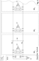
- Figure 2 shows a two-wire communication bus (DB) as is known from the prior art.
- the serial, bidirectional, differential two-wire communication bus (DB) consists of a first single-wire bus (DB a ) and a second single-wire bus (DB b ).
- the serial, bidirectional, differential two-wire communication bus connects the bus master (ECU) with several bus nodes ((BK 1 ) to [BK n ]).
- the bus master (ECU) has a first driver [TRa] with which it can bring the first single-wire bus (DB a ) into a first state (Z1) or a second state (Z2) or a third state (Z3).
- a first driver can preferably assume two of three permitted states as a CAN driver: In a first state, it applies a first logic level (Z1) to the first single-wire bus (DB a ). In a second state, it applies a third logic level (Z3) to the first single-wire bus (DB a ).
- the first driver of the bus master (ECU) also works in the addressing state of the data bus system and the bus nodes ((BK 1 ) to [BK n' ]) as the first current sink for the first addressing currents of the first Addressing current sources ((Iq 1 ) to [Iq n ]) of the bus nodes ((BK 1 ) to [BK n ]) and their first quiescent currents.
- the first driver of a bus node ((BK 1 ) to [BK n ]) or of the bus master (ECU) assumes the first state (Z1) when the second driver [TR b ] of the relevant bus node ((BK 1 ) to [BK n ]) assumes the second state (Z2).
- the signal is differentially impressed with a first differential level (z1).
- the first driver of a bus node ((BK 1 ) to [BK n ]) or of the bus master (ECU) assumes the third state (Z3) when the second driver (TR b ) of the relevant bus node ((BK 1 ) to [BK n ]) assumes the third state (Z3).
- the signal is differentially impressed with a third differential level (z3).
- the first driver can also preferably assume two of two permitted states as an RS485 driver: In a first state, it applies a first logic level (Z1) to the first single-wire bus (DB a ). In a second state, it applies a second logic level (Z2) to the first single-wire bus (DB a ).
- the first driver of the bus master (ECU) also works in the addressing state of the data bus system and the bus nodes ((BK 1 ) to [BK n ]) as the first current sink for the first addressing currents of the first addressing current sources ((Iq 1 ) to [Iq n ]) of the bus nodes ((BK 1 ) to [BK n ]) and their first quiescent currents.
- the first driver of a bus node ((BK 1 ) to [BK n ]) or of the bus master (ECU) assumes the first state (Z1) when the second driver [TR b ] of the relevant bus node ((BK 1 ) to [BK n ]) assumes the second state (Z2).
- the signal is differentially impressed with a first differential level (z1).
- the first driver of a bus node ((BK 1 ) to [BK n ]) or of the bus master (ECU) assumes the second state (Z2) when the second driver [TR b ] of the relevant bus node ((BK 1 ) to [BK n ]) assumes the first state (Z1).
- the signal is differentially impressed with a second differential level (z2).
- the first driver typically has a sub-device for detecting and avoiding a bus collision in the event of simultaneous access to the first single-wire bus (DB a ) by a first driver of another bus node ((BK 1 ) to [BK n ]) or the bus master (ECU).
- a second driver can preferably assume two of three permitted states as a CAN driver: In a first state, it applies a second logic level (Z2) to the second single-wire bus (DB b ). In a second state, it applies a third logic level (Z3) to the second single-wire bus (DB b ).
- the second driver of the bus master (ECU) also works in the addressing state of the data bus system and the bus nodes ((BK 1 ) to [BK n ]) as a second current sink for the second addressing currents of the second addressing current sources ((Iq' 1 ) to [Iq' n ]) of the bus nodes ((BK 1 ) to [BK n ]) and their second quiescent currents.
- the second driver of a bus node ((BK 1 ) to [BK n ]) or of the bus master (ECU) assumes the second state (Z2) when the first driver [TR a ] of the relevant bus node ((BK 1 ) to [BK n ]) assumes the first state (Z1).
- the signal is differentially impressed with a first differential level (z1).
- the second driver of a bus node ((BK 1 ) to [BK n ]) or of the bus master (ECU) assumes the third state (Z3) when the first driver [TR a ] of the relevant bus node ((BK 1 ) to (BK n ]) assumes the third state (Z3).
- the signal is differentially impressed with a third differential level (z3).
- the second driver can also preferably assume two of two permitted states as an RS485 driver: In a first state, it applies a second logic level (Z2) to the first single-wire bus (DB a ). In a second state, it applies a first logic level (Z1) to the second single-wire bus (DB b ).
- the second driver of the bus master (ECU) also works in the addressing state of the data bus system and the bus nodes ((BK 1 ) to [BK n ]) as a second current sink for the second addressing currents of the second addressing current sources ((Iq' 1 ) to [Iq' n ]) of the bus nodes ((BK 1 ) to [BK n ]) and their second quiescent currents.
- the second driver of a bus node ((BK 1 ) to [BK n ]) or of the bus master (ECU) assumes the second state (Z2) when the first driver [TR a ] of the relevant bus node ((BK 1 ) to [BK n ]) assumes the first state (Z1).
- the signal is differentially impressed with a first differential level (z1).
- the second driver of a bus node ((BK 1 ) to [BK n ]) or of the bus master (ECU) assumes the first state (Z1) when the first driver [TR a ] of the relevant bus node ((BK 1 ) to [BK n ]) assumes the second state (Z2).
- the signal is differentially impressed with a second differential level (z2).
- the second driver typically has a sub-device for detecting and avoiding a bus collision in the event of simultaneous access to the first single-wire bus (DB a ) by a second driver of another bus node ((BK 1 ) to [BK n ]) or the bus master (ECU).
- Each of the bus nodes ((BK 1 ) to [BK n ]) and the bus master (ECU) preferably have a receiver (Rec).
- the respective receiver (Rec) extracts the data (DATA) contained in the bit stream packets (BP) on the serial, bidirectional, differential two-wire communication bus (DB) and outputs these preferably together with error information via an output (out) of the receiver (Rec).
- the receiver (Rec) typically checks whether check information (CHKD) within data information (DATA) of a bit stream packet (BP) indicates error-free reception by the receiver (Rec). If a bit stream packet (BP) was not received error-free by the receiver (Rec), the receiver (Rec) preferably signals this.
- the data bus system has a common supply voltage line (V bat ) and typically a common reference potential [GND], which is Figure 2 is not shown.
- a device for controlling electrical and/or electronic bus nodes ((BK 1 ) to [BK n ]), in particular within a motor vehicle module, an interior light and/or an exterior light such as a rear light module of a motor vehicle, which has a serial, bidirectional, differential two-wire communication bus (DB) with n bus nodes (BK 1 to [BK n ]).
- DB serial, bidirectional, differential two-wire communication bus
- n is a positive integer greater than 1.
- the proposed device also has a bus master (ECU).
- the serial, bidirectional, differential communication bus (DB) consists of a first single-wire bus (DB a ) and a second single-wire bus (DB b ).
- Each bus node (BK j ) of the n bus nodes ((BK 1 ) to [BK n ]) has a differential, serial interface [IF j ] matching the serial, bidirectional, differential communication bus (DB).
- Each bus node (BK j ) of the n bus nodes ((BK 1 ) to [BK n ]) preferably has a clock generator [CLKG j ], a sampling device [AT j ], an address recognition unit [ADR;] and a bus node address register [BKADR;].
- the serial, The bidirectional, differential communication bus (DB) is designed in such a way that it can preferably be in at least a first logical state (high, Z1) and in a second logical state (low, Z2) and possibly in a third logical state (idle, Z3).
- levels of the high-speed CAN protocol [HS-CAN] can be used. This will be explained first.
- the serial, bidirectional, differential communication bus (DB) in the transmitters (TX a , TX b ) of the respective bus nodes (BK j ) is preferably clamped via a high-impedance voltage divider per transmitter (TX a , TX b ) to a preferably vanishing differential voltage difference between the first single-wire bus (DB a ) and the second single-wire bus (DB b ) corresponding to the third logical state (Idle, Z3).
- Each of the transmitters (TX a , TX b ) preferably comprises a switch with which, when activated, the first single-wire bus (DB a ) of the serial, bidirectional, differential communication bus (DB) is brought to the first logical state (High, Z1) by the first driver [TR a ] and the second single-wire bus (DB b ) of the serial, bidirectional, differential communication bus (DB) can be brought to a second logical state (Low, Z2) by the second driver (TR b ).
- the serial, bidirectional, differential communication bus (DB) in the transmitters (TX a , TX b ) of the respective bus node (BK j ) is preferably clamped to a differential voltage difference corresponding to the third logical state (idle, Z3) via a high-impedance voltage divider per transmitter (TX a , TX b ).
- Each of the transmitters (TX a , TX b ) preferably comprises a half-bridge with which the serial, bidirectional, differential communication bus (DB) can be brought to the first logical state (high, Z1) and a second logical state (low, Z2) by inverse control. If the half-bridges are switched off (IDLE), the serial, bidirectional, differential communication bus (DB) returns to the third logical state (idle, Z3).
- the serial interface (IF j ) of the at least one bus node (BK j ) of the n bus nodes ((BK 1 ) to [BK n ]) is connected to the serial, bidirectional, differential communication bus (DB) in order to send data via this serial, bidirectional, differential communication bus (DB) and/or to receive data from it. It typically comprises the aforementioned transmitters (TX a , TX b ) and a receiver (Rec) for each bus node (BK j ).
- the clock and data extraction within the bus nodes ((BK 1 ) to [BK n ]) from the bit packets (BP) is not shown in the drawings for the sake of simplicity, since it can be taken from the prior art.
- the bus master (ECU) receives external control commands for the n bus nodes ((BK 1 ) to [BK n ]) and converts these control commands into bit streams to be sent to the bus nodes ((BK 1 ) to [BK n ]) via the serial, bidirectional, differential communication bus (DB).
- the bus master (ECU) sends the bits of the bit streams to be sent by the bus master (ECU) via the serial, bidirectional, differential communication bus (DB) depending on a clock pulse (CLK) within the bus master (ECU).
- the bus master (ECU) receives bit streams generated in the opposite direction by the bus nodes ((BK 1 ) to [BK n ]) via the serial, bidirectional, differential communication bus (DB).
- Clock generators [CLKG j ] within each bus node (BK j ) of the n bus nodes ((BK 1 ) to [BK n ]) generate a respective sampling signal [CLKA j ] within each bus node (BK j ) of these bus nodes ((BK 1 ) to [BK n ]).
- the sampling device [AT j ] of this respective bus node (BK j ) of the n bus nodes ((BK 1 ) to [BK n ]) then samples the bit streams sent via the serial, bidirectional, differential communication bus (DB) depending on the sampling signal [CLKA j ] of this bus node (BK j ).
- bus nodes can be bit streams from the bus master (ECU) to the bus nodes ((BK 1 ) to [BK n ]) as well as bit streams from the other bus nodes ((BK 1 ) to [BK n ]) to the bus master (ECU) or to other bus nodes ((BK 1 ) to [BK n ]).
- the bus node in question (BK j ) extracts in this way from the signals on the serial, bidirectional, differential communication bus (DB) a local bit stream within this bus node (BK j ), from the output of the receiver (Rec) by sampling the output signal of the receiver (Rec) or a signal derived from it.
- DB serial, bidirectional, differential communication bus
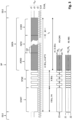
- the bus master sends the bit streams to be sent as sequences of bits in bit stream packets (frames, BP).
- the bus nodes also prefer to send their bit streams as sequences of bits in bit stream packets (frames, BP), which preferably correspond in structure to those of the bus master (ECU). For simplicity, only the bit stream packets are shown here. (English frames, BP) of the bus master (ECU) are discussed. The same applies to the bit stream packets (BP) of the bus nodes ((BK 1 ) to [BK n ]).
- this structure means that when neither the bus master (ECU) nor any of the n bus nodes ((BK 1 ) to [BK n ]) transmits data over the serial, bidirectional, differential two-wire communication bus (DB), the serial, bidirectional, differential two-wire communication bus (DB) assumes the first logic state (Z1) (dashed in Figure 3 ) or the third logical state (Z3) - which is preferred.
- V diff represents the differential level on the serial, bidirectional, differential communication bus (DB), i.e. the voltage difference between the first single-wire bus (DB a ) and the second single-wire bus (DB b ).
- HS-CAN describes the corresponding single levels as well as differential levels when CAN drivers [TR a , TR b ] are used.
- RS485 shows the corresponding single levels as well as differential levels when RS485 drivers [TR a , TR b ] are used.
- the drivers [TR a , TR b ] provide three voltage levels in the HS-CAN scheme, but only two differential voltage levels.
- the drivers (TR a , TR b ) provide two voltage levels and only two differential voltage levels in the RS485 scheme.
- the address recognition units ([Adr 1 ] to [Adr n ]) of the bus nodes ((BK 1 ) to [BK n ]) only allow the contained useful information (INFO) to be used if the content of the address information (ADRD) corresponds to the content of the bus node address register [BKADR j ] of the bus node (BK j ).
- the bus nodes (BK j ) of the n bus nodes ((BK 1 ) to [BK n ]) have means for carrying out an auto-addressing method for a two-wire data bus in order to fill the bus node address register [BAKDR;] with a logical bus node address which corresponds to the physical position of this bus node (BK j ) of the n bus nodes ((BK 1 ) to [BK n ]) within the serial, bidirectional, differential two-wire communication bus (DB).
- BAKDR bus node address register
- DB serial, bidirectional, differential two-wire communication bus
- each bus node (BK j ) of the n bus nodes has a microcontroller [ ⁇ C j ], which can take over some of the previously mentioned tasks, such as those of the address recognition unit [ADR j ] of the respective bus node (BK j ) and/or the scanning device [AT j ] of the respective bus node (BK j ) via a software program.
- At least one bus node (BK j ) of the n bus nodes ((BK 1 ) to [BK n ]) additionally has at least one light source [LED;] and at least one energy supply means [EV j ].
- the at least one energy supply means [EV j ] of the at least one bus node (BK j ) of the n bus nodes ((BK 1 ) to [BK n ]) is then provided for the energy supply of the at least one light source [LED j ] of the at least one bus node (BK j ) of the n bus nodes ((BK 1 ) to [BK n ]).
- At least part of the useful information (INFO) includes lighting information (ILD) for controlling the energy supply of the lamps [LED j ] of the bus node (BK j ) by the energy supply means [EV j ] of the bus node (BK j ) depending on this lighting information.
- ILD lighting information
- a lighting register within the energy supply means [EV j ] is typically written with a value depending on the received lighting information (ILD), which determines the radiation properties such as color, color temperature and brightness of the connected light source [LED j ].
- the logical content of the address information (ADRD) must match the content of the bus node address register [BKADR j ] of the bus node (BK j ). If this is not the case, the data information (DATA) is ignored. The same applies if checking the integrity of the received data information (DATA) using the test data (CHKD) that is also received shows that the reception was faulty.
- the respective address recognition unit [ADR j ] of the respective bus node (BK j ) evaluates the address information (ADRD) of a received bit stream packet (BP) and only allows the contained useful information (INFO) to be used by the rest of the bus node devices of the bus node (BK j ) if the content of the received address information (ADRD) corresponds to the content of the bus node address register [BKADR j ] of the bus node (BK j ) and is error-free.
- bus nodes ((BK 1 ) to [BK n ]) have means for carrying out an auto-addressing method for a serial, bidirectional and differential communication bus (DB).
- the bus node address register [BAKDR;] of these bus nodes ((BK 1 ) to [BK n ]) is filled with a logical bus node address which corresponds to the physical position of this bus node (BK j ) of the n bus nodes ((BK 1 ) to [BK n ]) within the serial, bidirectional, differential two-wire communication bus (DB).
- the bus master (ECU) and/or bus nodes ((BK 1 ) to [BK n ]) are equipped with means to conclude, based on the evaluation of the test information (CHKD), that the clock generator [CLKG j ] of one or more bus nodes (BK j ) is not running correctly.
- bus nodes ((BK 1 ) to [BK n ]) determine their physical position within the data bus system in the serial, bidirectional, differential two-wire communication bus (DB) and receive a bus node address based on it, so that the logical address corresponds to the physical address.
- DB serial, bidirectional, differential two-wire communication bus
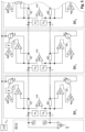
- a first bus shunt resistor (R2) is inserted into the first single-wire bus (DB a ) for each bus node ((BK 1 ) to [BK n ]).
- a second differential amplifier (D2) is used to measure the first current through the first single-wire bus (DB a ) by means of the first shunt resistor (R2).
- the output of the second differential amplifier (D2), which is used to measure the first current through the first single-wire bus (DB a ) is connected to a third comparator (D3), which compares the output value of the second differential amplifier (D2) with a first reference value (Ref).
- the data bus system with its bus nodes ((BK 1 ) to [BK n ]) can now be put into an addressing state and a normal state by the bus master (ECU) using a special bus signal. During the addressing state, an auto-addressing process is carried out. If the data bus system is in the addressing state, the bus nodes ((BK 1 ) to [BK n ]) that can carry out the auto-addressing process are in a corresponding addressing state of the bus nodes.
- the first addressing current source (Iq j ) (with 1 ⁇ j ⁇ n) of the respective bus node (BK j ) is switched off in the normal state or fulfills another function such as supplying power to a light source [LED j ].
- the first addressing current source (Iq j ) (with 1 ⁇ j ⁇ n) of the respective bus node (BK j ) is switched off in the addressing state if the respective bus node (BK j ) detects by means of these first means (R2, D2, D3) a first current through its first bus shunt resistor (R2) which is above a threshold value corresponding to the first reference current [I Ref ].
- the respective first addressing current source (Iq j ) of a bus node (BK j ) feeds its first addressing current into the first single-wire bus (DB a ) before the respective first bus shunt resistor (R2) of the respective bus node (BK j ) as seen from the bus master (ECU), if the bus node (BK j ) determines by means of the first means (R2, D2, D3) described above that only a first current below this threshold value flows through its first bus shunt resistor (R2) in the direction of the bus master (ECU).
- This has the disadvantage that a self-test of the bus node (BK j ) at this feed-in point of the first addressing current is not possible.
- the first driver [TR a ] of the bus master (ECU) may be overloaded during the switch-on process. Therefore, the first addressing current of the first addressing current sources ((Iq 1 ) to [Iq n ]) must be limited to an n-th part of the maximum current value that the first driver [TR a ] can still absorb. This limits the resistance value of the first bus shunt resistor (R2) downwards, since otherwise the level of the voltage drop across the first bus shunt resistor (R2) of a bus node (BK j ) would be too small for detection by the first means (R2, D2, D3) of this bus node (BK j ). This leads to increased sensitivity to electromagnetic radiation, which is actually what should be avoided.
- a bus node (BK j ) in the addressing state determines, after a certain, predetermined waiting time after entering the addressing state, that its first addressing current source (Iq j ) has not yet been switched off, then it is the last bus node (BK;) not yet provided with a valid bus node address. It then adopts a bus node address to be assigned, typically offered by the bus master (ECU), as its new valid bus node address.
- the bus node [BK j-1 ] which is the next bus node to determine in the next initialization run that its addressing current source (Iq j ) is not switched off, then takes the next bus node address to be assigned offered by the bus master (ECU) as its valid bus node address and so on. This continues until all bus nodes ((BK 1 ) to [BK n ]) of the data bus system have received a valid bus node address in this way.
- the bus master then typically returns the data bus system and its bus nodes ((BK 1 ) to [BK n ]) to the normal state, whereby the valid bus node addresses are retained.
- This recommended retention of the valid bus node addresses when transitioning from the addressing state to the normal state applies preferably to the entire document.
- DB serial, bidirectional, differential two-wire communication bus
- DB a and DB b the two single-wire buses
- the data bus system should therefore have bus nodes (BK j ) with a first bus shunt resistor (R2) inserted into the first single-wire bus (DB 1 ) and a second single-wire bus (DB 2 ) for the two-wire communication bus (DB), which consists of a first single-wire bus (DB 1 ) and a second single-wire bus (DB 2 ), and a second bus shunt resistor (R2') inserted into the second single-wire bus (DB 2 ).
- DB bus nodes
- R2 bus shunt resistor
- the two bus shunt resistors (R2, R2') per bus node (BK j ) of the bus nodes ((BK 1 ) to [BK n ]) are preferably monolithically integrated and manufactured to match with a relative resistance value deviation within the respective bus node (BK j ) of less than 10% and/or better less than 5% and/or better less than 2% and/or better less than 1% and/or better less than 0.5%.
- Each bus node (BK j ) is now equipped, in addition to the first means (R2, D2, D3) for detecting the first current through the first bus shunt resistor (R2) in the first single-wire bus (DB a ), with second means (R2', D2', D3') for detecting the second current through the second bus shunt resistor (R2') in the second single-wire bus (DB b ).
- a second bus shunt resistor (R2') is inserted into the second single-wire bus (DB b ) for each bus node ((BK 1 ) to [BK n ]).
- a further second differential amplifier (D2') is used to measure the second current through the second single-wire bus (DB b ) using the second shunt resistor (R2') of the relevant bus node (BK j ).
- the output of the further second differential amplifier (D2'), which is used to measure the second current through the second single-wire bus (DB b ), is connected to a further third comparator (D3'), which compares the output value of the further second differential amplifier (D2') with a further reference value (Ref), which is typically equal to the previously mentioned reference value (Ref).
- the second addressing current source (Iq' j ) (with 1 ⁇ j ⁇ n) of the respective bus node (BK j ) is switched off when the respective bus node (BK j ) detects by means of these second means (R2', D2', D3') a first current through its second bus shunt resistor (R2') which is above a threshold value corresponding to the first reference current [I Ref ].
- the respective second addressing current source (Iq' j ) of a bus node (BK j ) also feeds the second addressing current into the second single-wire bus (DB b ) before the respective second bus shunt resistor (R2') of the respective bus node (BK j ) as seen from the bus master (ECU), if the bus node (BK j ) determines by means of the previously described second means (R2', D2', D3') that only a second current below this threshold value is flowing through its second bus shunt resistor (R2') in the direction of the bus master (ECU).
- both addressing current sources (Iq j , Iq' j ) of a bus node (BK j ) are always switched off when the bus node (BK j ) determines by means of the previously described first means (R2, D2, D3) that a first current above the threshold value is flowing through its first bus shunt resistor (R2) in the direction of the bus master (ECU) or determines by means of the previously described second means (R2', D2', D3') that only a second Current above this threshold flows through its second bus shunt resistor (R2') towards the bus master (ECU).
- Figure 6 now shows another suggestion based on the Figure 5 .
- Essential difference to Figure 5 is that the respective first addressing current sources ((Iq 1 ) to [Iq n ]) as seen from the bus master (ECU) feed the first addressing current behind the first bus shunt resistors (R2) in the addressing phase in which the respective bus node (BK j ) is in an addressing state, if the respective bus node (BK j ) determines by means of the first means (R2, D2, D3) a current value of the first current through the first bus shunt resistor (R2) that is smaller than a predetermined first reference current value [I ref ].
- the third comparator (D3) is preferably now a third differential amplifier (D3).
- the respective second addressing current sources ((Iq' 1 ) to [Iq' n ]) as seen from the bus master (ECU) also apply the respective second addressing current behind the corresponding second bus shunt resistors (R2') in the addressing phase in which the respective bus node (BK j ) is in an addressing state, if the respective bus node (BK j ) determines by means of the second means (R2', D2', D3') a current value of the second current through the second bus shunt resistor (R2) that is smaller than a predetermined second reference current value [I' ref ], which is preferably equal to the first reference current value [I ref ].
- the further third comparator (D3') is preferably now a further third differential amplifier (D3').
- the second addressing current of the respective second addressing current source (Iq' j ) of the respective bus node (BK j ) is now also adjusted until the second current through the second bus shunt resistor (R2') corresponds to the predetermined second reference current [I' ref ].
- the bus node (BK j ) is thus provided with a first addressing current source (Iq j ) for determining the bus position of the bus node (BK j ) in the serial, bidirectional, differential two-wire communication bus (DB), which can additionally feed a first addressing current into the first single-wire bus (DB a ) of the serial, bidirectional, differential two-wire communication bus (DB) in a controlled manner such that the first total current (i j ) through the first bus shunt resistor (R2) of the bus node (BK j ) corresponds to a predetermined or calculated or otherwise determined first total current [I ref ].
- the first addressing current preferably flows through the first bus shunt resistor (R2).
- the respective bus node (BK j ) is now provided with a second addressing current source (Iq' j ) for determining the bus position of the bus node (BK j ) in the serial, bidirectional, differential two-wire communication bus (DB), which can additionally feed a second addressing current into the second single-wire bus (DB b ) of the serial, bidirectional, differential two-wire communication bus (DB) in a controlled manner such that the second total current (i j ) through the second bus shunt resistor (R2') of the bus node (BK j ) corresponds to a predetermined or calculated or otherwise determined second total current [I' ref ].
- Iq' j second addressing current source
- the second addressing current now flows through the second bus shunt resistor (R2').
- R2' the second bus shunt resistor
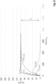
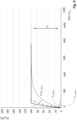
- the Figures 7 to 9 represent advantageous properties of the control.
- the control is explained using the example of the first addressing current sources ((Iq 1 ) to [Iq n ]), but also applies to the second addressing current sources ([Iq' 1 ] to [Iq' n ]) in an analogous manner.
- the units for the abscissa and ordinate are designated with [an] as a placeholder for an arbitrary unit.
- the control characteristic for the first addressing current source (Iq j ) of a bus node (Bk j ) is preferably generated in each case by a first filter (F) or a first controller, which generates a first control signal [rw j ] from the output signal of the third differential amplifier (D3), with which the first addressing current source (Iq j ) of the relevant bus node (BK j ) is controlled.
- the control characteristic for the second addressing current source (Iq' j ) of a bus node (Bk j ) is preferably generated in each case by a second filter (F) or a second controller, which generates a second control signal (rw' j ) from the output signal of the further third differential amplifier (D3'), with which the second addressing current source (Iq' j ) of the relevant bus node (BK j ) is controlled.
- the time constants for the increase in the first addressing current of the first addressing current sources and the decrease in the first addressing current of the first addressing current sources are approximately the same. An overshoot occurs.
- the first addressing current (I 1_internal ) of the first addressing current source (Iq 1 ) of the first bus node (BK 1 ) and the first addressing current (I 2_internal ) of the first addressing current source (Iq 2 ) of the second bus node (BK 2 ) are regulated down by the regulators of these first auto-addressing bus nodes, while the first addressing current (I 3_internal ) of the first addressing current source (Iq 3 ) of the third bus node (BK 3 ) is regulated to the reference value [I ref ].
- the settling time is determined by a first time constant [ ⁇ 1 ] for increasing the first addressing current of the first addressing current sources (Iq 1 to Iq 3 ).
- Figure 8 shows the course of the output current (i 1 ) of the first bus node (BK 1 ), the output current (i 2 ) of the second bus node (BK 2 ) and the output current (i 3 ) of the third bus node (BK 3 ). It also shows the current (I 1_internal ) of the first addressing current source (Iq 1 ) of the first bus node (BK 1 ), the current (I 2_internal ) of the first addressing current source (Iq 2 ) of the second bus node (BK 2 ) and the current (I 3_internal ) of the first addressing current source (Iq 3 ) of the third bus node (BL 3 ).
- the first time constants [ ⁇ 1 ] for the increase in the first addressing current of the first addressing current sources are approximately ten times as long as the second time constants [ ⁇ 2 ] for the decrease in the first addressing current of the first addressing current sources. Only a minimal overshoot occurs.
- Figure 9 shows the course of the output current (i 1 ) of the first bus node (BK 1 ), the output current (i 2 ) of the second bus node (BK 2 ) and the output current (i 3 ) of the third bus node (BK 3 ). It also shows the first addressing current (I 1_internal ) of the first addressing current source (Iq 1 ) of the first bus node (BK 1 ), the first addressing current (I 2_internal ) of the first addressing current source (Iq 2 ) of the second bus node (BK 2 ) and the first addressing current (I 3_internal ) of the first addressing current source (Iq 3 ) of the third bus node (BK 3 ).
- the first time constants [ ⁇ 1 ] for the increase in the first addressing current of the first addressing current sources are approximately one hundred times as long as the second time constants [ ⁇ 2 ] for the decrease in the first addressing current of the first addressing current sources. There is no overshoot.
- the bus node (BK j ) comprises first means (R2, D2) for detecting the current through the first bus shunt resistor (R2) and/or second means (R2', D2') for detecting the current through the second bus shunt resistor (R2').
- the data bus system is designed in such a way that the first and second addressing current of the two addressing current sources (Iq j , Iq' j ) are always fed in behind the bus shunt resistors (R2, R2') as seen from the bus master (ECU), the current detected by the first bus shunt resistor (R2) and/or the second bus shunt resistor (R2') can be used for a self-test.
- both voltage drops across both Bus shunt resistors (R2, R2') should preferably be equal. A cold solder joint, for example, can therefore be easily detected in this way.
- the bus node (BK j ) with a first detection device (DET) that checks the internal signals (ds1, ds3) of the bus node (BK j ) for plausibility.
- the internal signals are preferably control signals within the bus node (BK j ).
- bus symmetry for example, the symmetry of these signals can be checked.
- tests per channel are also possible.
- the first detection device changes the feed point for the first addressing current of the regulated first addressing current source (Iq j ) of the j-th bus node (BK j ), for example with the aid of a first analog demultiplexer (X3), and swaps the polarity of the inputs or the output of the second differential amplifier (D2) by means of the polarity signal (pol).
- the second detection device can, for example, change the feed point for the second addressing current of the regulated second addressing current source (Iq' j ) of the j-th bus node (BK j ), for example with the aid of a second analog demultiplexer (X3'), and swap the polarity of the inputs or the output of the further second differential amplifier (D2') by means of a second polarity signal (pol').
- a reparameterization of internal sub-devices such as current sources for neutralizing the error is possible if, instead of a first addressing current source (Iq j ) of the j-th bus node (BK j ) and a first multiplexer (X3), a first addressing current source [Iq j1 ] of the j-th bus node (BK j ) and, for example, a further first addressing current source [Iq j2 ] of the j-th bus node (BK j ) are used, of which the first addressing current source [Iq j1 ] of the j-th bus node (BK j ) feeds its first addressing current before the first bus shunt resistor (R2) and the further first Addressing current source [Iq j2 ] of the j-th bus node (BK j ) feeds its further first addressing current behind the first bus shunt resistor (
- the first detection device would set the first addressing current of one of the two first addressing current sources ([Iq j1 ], [Iq j2 ]) to zero, so that the equivalent effect is achieved as with the combination of a first addressing current source (Iq j ) of the j-th bus node (BK j ) with the switching by a first demultiplexer (X3).
- a second addressing current source [Iq' j1 ] of the j-th bus node (BK j ) and, for example, a further second addressing current source [Iq' j2 ] of the j-th bus node (BK j ) would be used, of which the second addressing current source [Iq' j1 ] of the j-th bus node (BK j ) feeds its second addressing current upstream of the second bus shunt resistor (R2') and the further second addressing current source [Iq' j2 ] of the j-th bus node (BK j ) feeds its further second addressing current downstream of the second bus shunt resistor (R2').
- the second detection device would set the second addressing current of one of the two second addressing current sources ([Iq' j1 ], [Iq' j2 ]) to zero, so that the equivalent effect is achieved as in the combination of a second addressing current source (Iq' j ) of the j-th bus node (BK j ) with the switching by a further second demultiplexer (X3').
- the first detection device can recognize that the first control value of the first control signal (rw j ) of the j-th bus node (BK j ) maximizes the first addressing current of the first addressing current source (Iq j ). This can be done, for example, with a suitable design, by comparing the first control value of the first control signal (rw j ) with a tenth threshold value (Ref10). If the derivative of the first addressing current of the first auto-addressing current source (Iq j ) with respect to the first control value of the first control signal (rw j ) is positive, this means that the first control value of the first control signal (rw j ) is above the tenth threshold value (Ref10).
- the first detection device (DET) can simultaneously compare the output (ds2) of the second differential amplifier (D2) with an eleventh threshold value (Ref11). If the value of the output (ds2) of the second differential amplifier (D2) is below the eleventh threshold value (Ref11), the first detection device (DET) can conclude that there is a negative voltage drop across the first bus shunt resistor (R2) or that there is a voltage drop across the first bus shunt resistor (R2) close to zero. This state is illegal because the first auto-addressing current source (Iq j ) supplies a positive first addressing current, which, if correctly mounted, should flow through the first bus shunt resistor (R2), but this obviously does not happen.
- Iq j the first auto-addressing current source
- the second detection device can also detect that the second control value of the second control signal (rw' j ) of the j-th bus node (BK j ) maximizes the second addressing current of the second addressing current source (Iq' j ). This can be done, for example, with a suitable design, by comparing the second control value of the second control signal (rw' j ) with a further tenth threshold value (Ref10'), which is preferably equal to the tenth threshold value (Ref10).
- a further tenth threshold value (Ref10')
- the second detection device (DET) can simultaneously compare the further output (ds2') of the further second differential amplifier (D2') with a further eleventh threshold value (Ref11').
- the further eleventh threshold value (Ref11') is preferably equal to the eleventh threshold value (Ref11).
- the second detection device can conclude that there is a negative voltage drop across the second bus shunt resistor (R2') or that there is a voltage drop across the second bus shunt resistor (R2') close to zero.
- This state is illegal because the second auto-addressing current source (Iq' j ) supplies a positive second addressing current, which, if correctly mounted, should flow through the second bus shunt resistor (R2'), but this obviously does not happen.
- the first detection device (DET) and the second detection device (DET) form a unit.
- Switching the bus direction preferably only occurs when both detection devices (DET, DET) detect a swap of the bus connections.
- the detection devices can signal a detected error, for example, via a respective error signal (er, er') to a bus node internal computer or a suitable controller.
- the test results can be used by the bus node (BK j ) or a sub-device (DET, DET) of the bus node (BK j ) to initiate and take predetermined measures if one or more of the detection devices (DET, DET) detect implausible internal signals within the bus node (BK j ).
- the bus node (BK j ) can assume that the input and output have been swapped.
- the bus node (BK j ) has a first sub-device (X3) which can change the feed point of the first addressing current of the first addressing current source (Iq j ) and/or if the bus node (BK j ) has a second sub-device (X3') which can change the feed point of the second addressing current of the second addressing current source (Iq' j ).
- the changes for controlling the first single-wire bus (DB a ) and the first bus shunt resistor (R2) are carried out synchronously with the analog changes for controlling the second single-wire bus (DB b ) and the second bus shunt resistor (R2').
- Such a bus node (BK j ) therefore has, instead of a first addressing current source (Iq j ), a first addressing current source and a further first addressing current source, the first addressing current source feeding its first addressing current into a node connected to the first terminal of the first bus shunt resistor (R2) when it feeds in current, and the further first addressing current source feeding its first addressing current into a node connected to the second terminal of the first bus shunt resistor (R2) when it feeds in current.
- the two first addressing current sources preferably feed their addressing currents in such a way that the resulting total addressing current flows through the first bus shunt resistor (R2), which ensures the self-testing capability.
- the bus node (BK j ) has, instead of a second addressing current source, a second addressing current source and a further second addressing current source, the second addressing current source feeding its addressing current into a node connected to the first terminal of the first bus shunt resistor (R2). the first terminal of the second bus shunt resistor (R2') when it feeds current, and wherein the further second addressing current source feeds its addressing current into a node connected to the second terminal of the second bus shunt resistor (R2') when it feeds current.
- These two second addressing current sources also preferably feed their addressing currents in such a way that the addressing current flows through the second bus shunt resistor (R2') in order to ensure the self-test capability.
- the first addressing current source (Iq j ) increases the first addressing current with a first time constant [ ⁇ 1 ] and decreases it with a second time constant [ ⁇ 2 ] that is smaller than the first time constant [ ⁇ 1 ] and/or if the second addressing current source (Iq' j ) increases the second addressing current with a third time constant [ ⁇ 3 ] and decreases it with a fourth time constant [ ⁇ 4 ] that is smaller than the third time constant [ ⁇ 3 ].
- the third time constant [ ⁇ 3 ] and the first time constant [ ⁇ 1 ] are preferably selected to be the same amount in order to ensure bus symmetry dynamically as well.
- the fourth time constant [ ⁇ 4 ] and the second time constant [ ⁇ 2 ] are preferably chosen to have the same amount in order to ensure dynamic bus symmetry here too.
- the bus node (BK j ) described above is therefore a bus node (BK j ) which is capable of carrying out a method for assigning bus addresses to bus nodes of a serial, bidirectional, differential two-wire communication bus (DB).
- the method for assigning bus addresses to bus nodes ((BK 1 ), (BK 2 ), (BK 3 ), whil [BK n-1 ], [BK n ]) of a serial, bidirectional, differential two-wire communication bus (DB) is carried out with the aid of first bus shunt resistors (R2) and with the aid of second bus shunt resistors (R2') in the individual bus nodes ((BK 1 ), (BK 2 ), (BK 3 ), «
- the bus node (BK j ) is thus characterized in comparison to the prior art by such a first bus shunt resistor (R2) and such a second bus shunt resistor (R2').
- the bus node (BK j ) is provided with a first bus shunt bridging switch (S4) which is open before a bus address is assigned to the bus node (BK j ) in the allocation period and which is closed after a bus address is assigned to the bus node in the allocation period and which is closed during the operating period.
- a second bus shunt bridging switch (S4') is preferably provided in the bus node (BK j ), which is open before a bus address is assigned to the bus node (BK j ) in the allocation period and which is closed after a bus address is assigned to the bus node (BK j ) in the allocation period and which is closed during the operating period.
- These bus shunt bridging switches (S4, S4') massively reduce the bus resistance and reduce the sensitivity to electromagnetic radiation. They therefore improve the EMC behavior.
- a common-mode current source [GLIq j ] of a bus node (BK j ) with two outputs can also be used, both of which feed the same amount of common-mode current into the first single-wire bus (DB a ) and the second single-wire bus (DB b ) of the serial bidirectional differential communication bus (DB) with the same sign.
- a first output of these two outputs therefore corresponds to the first addressing current source (Iq j ).
- the second output then corresponds to the second addressing current source (Iq' j ).
- the first addressing current of the first addressing current source (Iq j ) is then equal in amount to the second addressing current of the second addressing current source (Iq' j ).
- the use of a single common-mode addressing current source [GLIq j ] has the advantage that only one control loop is required.
- a push-pull current source [GGIq j ] of a bus node (BK j ) with two outputs can also be used, both of which feed the same amount of push-pull current into the first single-wire bus (DB a ) and the second single-wire bus (DB b ) of the serial bidirectional differential communication bus (DB), but now with a different sign.
- a first output of these two outputs therefore corresponds to the first addressing current source (Iq j ).
- the second output then corresponds again to the second addressing current source (Iq' j ).
- the first addressing current of the first addressing current source (Iq j ) is then equal in amount but not the same sign as the second addressing current of the second addressing current source (Iq' j ).
- the use of a single push-pull addressing current source[GLIq j ] also has the advantage that only one control loop is required.
- a bus node (BK j ) for a serial, bidirectional, differential two-wire communication bus (DB) with a bus master (ECU) is also proposed here, in which the serial, bidirectional, differential two-wire communication bus (DB) comprises a first single-wire bus (DB 1 ) and a second single-wire bus (DB 2 ).
- a first bus shunt resistor (R2) inserted into the first single-wire bus (DB 1 ) and a second bus shunt resistor (R2') inserted into the second single-wire bus (DB 2 ) are part of the bus node (BK;).
- the bus node further comprises a differential first common-mode addressing current source [GLIq j ] for determining the bus position of the bus node (BK j ) in the serial, bidirectional, differential two-wire communication bus (DB).
- the differential first common-mode addressing current source [GLIq j ] can additionally feed a first common-mode addressing current component into the first single-wire bus (DB a ) of the serial, bidirectional, differential two-wire communication bus (DB) in a controlled manner such that the first total current (i j ) through the first bus shunt resistor (R2) of the bus node (BK j ) corresponds to a predetermined or calculated or otherwise determined first total current [I ref ].
- the differential first common-mode addressing current source [GLIq j ] can additionally feed a second common-mode addressing current component with the same amount and sign into the second single-wire bus (DB b ) of the serial, bidirectional, differential two-wire communication bus (DB) in a regulated manner with the same sign as the sign of the first differential-mode addressing current component, so that the second total current (i' j ) through the second bus shunt resistor (R2') of the bus node (BK j ) also corresponds to the predetermined or calculated or otherwise determined first total current [I ref ].
- the first common-mode addressing current component of the common-mode addressing current source [GLIq j ] of the bus node (BK j ) flows through the first bus shunt resistor (R2) of the bus node (BK j ) in the direction of the bus master (ECU).
- the second common-mode addressing current component of the common-mode addressing current source [GLIq j ] of the bus node (BK j ) flows through the second bus shunt resistor (R2') of the bus node (BK j ) in the direction of the bus master (ECU).
- a bus node (BK j ) for a serial, bidirectional, differential two-wire communication bus (DB) with a bus master (ECU) is therefore proposed, in which the serial, bidirectional, differential two-wire communication bus (DB) comprises a first single-wire bus (DB 1 ) and a second single-wire bus (DB 2 ) and in which a first bus shunt resistor (R2) is inserted into the first single-wire bus (DB 1 ) and a second bus shunt resistor (R2') is inserted into the second single-wire bus (DB 2 ).
- the bus node (BK j ) then has a differential first push-pull addressing current source [GGIq j ] for determining the bus position of the bus node (BK j ) in the serial, bidirectional, differential two-wire communication bus (DB), which has a first Push-pull addressing current component can be additionally fed into the first single-wire bus (DB a ) of the serial, bidirectional, differential two-wire communication bus (DB) in a controlled manner such that the first total current (i j ) through the first bus shunt resistor (R2) of the bus node (BK j ) corresponds to a predetermined or calculated or otherwise determined first total current [I ref ].
- GGIq j differential first push-pull addressing current source
- the push-pull addressing current source [GGIq j ] of the bus node (BK j ) feeds the second push-pull addressing current component, which is the same in magnitude, into the second single-wire bus (DB b ) of the serial, bidirectional, differential two-wire communication bus (DB) in a regulated manner with the opposite sign to the sign of the first push-pull addressing current component, so that the second total current (i' j ) through the second bus shunt resistor (R2') of the bus node (BK j ) also corresponds to the predetermined or calculated or otherwise determined first total current [I ref ].
- the first push-pull addressing current component of the push-pull addressing current source [GGIq j ] of the bus node (BK j ) flows through the first bus shunt resistor (R2) of the bus node (BK j ) in the direction of the bus master (ECU).
- the second push-pull addressing current component of the push-pull addressing current source [GGIq j ] of the bus node (BK j ) flows through the second bus shunt resistor (R2') of the bus node (BK j ) in the direction of the bus master (ECU).
- the bus node (BK j ) preferably has first means (R2, D2) to detect the current through the first bus shunt resistor (R2) and/or second means (R2', D2') to detect the current through the second bus shunt resistor (R2').
- the ability to detect the voltage drop across the respective bus shunt resistor (R2, R2') can also be used for a self-test.
- a bus node (BK j ) is therefore proposed in which the detected current through the first bus shunt resistor (R2) is used for a self-test and/or in which the detected current through the second bus shunt resistor (R2') is used for a self-test.
- the detected voltage drop across the bus shunt resistor is compared with an expected value. If the detected voltage deviates from the expected value by more than a predetermined amount, an error has occurred that can be signaled.
- the proposed bus node (BK j ) preferably comprises at least one detection device (DET) which detects internal signals (ds1, ds3) of the bus node (BK j ) for plausibility.
- the bus node (BK j ) or a sub-device (DET) of the bus node (BK j ) takes measures if the detection device (DET) detects implausible internal signals within the bus node (BK j ).
- One possible measure can be initiated by a first sub-device (X3) of the bus node (BK j ) and a second sub-device (X3') of the bus node (BK j ) in such a way that the feed points of the first common-mode addressing currents of the common-mode addressing current source [GLIq j ] are changed by the first sub-device (X3) of the bus node (BK j ) and the second sub-device (X3') of the bus node (BK j ) when a predetermined error is detected.
- Another possible measure can be initiated by a first sub-device (X3) of the bus node (BK j ) and a second sub-device (X3') of the bus node (BK j ) in such a way that the feed points of the first push-pull addressing currents of the push-pull addressing current source [GGIq j ] are changed by the first sub-device (X3) of the bus node (BK j ) and the second sub-device (X3') of the bus node (BK j ) upon detection of a predetermined error.
- a bus node (BK j ) is therefore proposed in which the common-mode addressing current source [GLIq j ] increases the common-mode addressing current with a first time constant [ ⁇ 1 ] and decreases it with a second time constant [ ⁇ 2 ] which is smaller than the first time constant [ ⁇ 1 ].
- a bus node (BK j ) is therefore proposed in which the push-pull addressing current source [GGIq j ] increases the push-pull addressing current with a first time constant [ ⁇ 1 ] and decreases it with a second time constant [ ⁇ 2 ] which is smaller than the first time constant [ ⁇ 1 ].
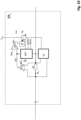
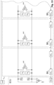
- the bus node (BK j ) described above which is intended for a data bus system with a serial, bidirectional, differential two-wire communication bus (DB), can be used for another auto-addressing method (see Figure 13 ) prepared
- the relevant bus node (BK j ) is then again intended to participate in a process for assigning logical bus node addresses to the bus nodes ((BK 1 ) to [BK n ]) of the data bus system.
- the relevant data bus system then has a bus master (ECU) with an address input (Adr i0 ).
- the data bus system should again have n bus nodes ((BK 1 ) to [BK n ]) including this bus node (BK j ) itself, with n as a positive integer.
- the bus node (BK j ) is connected to the bus master (ECU) for data transmission via a data line section ((DB 1 ) to [DB n ]) or the serial, bidirectional, differential two-wire communication bus (DB) consisting of data line sections ((DB 1 ) to [DB n ]) and further bus nodes ((BK 2 ) to [BK n ]).
- a line [L 1 to L n ] is looped from an address input (Adno) of the bus master (ECU) of the data bus system through all bus nodes ((BK 1 ) to [BK n ]) of the data bus system, including this bus node (BK j ) itself, in such a way that it is divided into n line sections [L 1 to L n ] by the individual bus nodes ((BK 1 ) to [BK n ]), including this bus node (BK j ) itself.
- Each of the bus nodes (BK j ) comprises an associated address input [Adr ij ] and an address output [Adr oj ] associated with this bus node (BK j ).
- the bus node address of the bus node (BK j ) in its bus node address register [BKADR j ] can be valid or invalid, as in this entire document.
- the proposed bus node now provides means and methods to set its bus node address and to make its bus node address valid or invalid.
- the proposed bus node (BK j ) can assume an addressing state and a second operating state (or normal state) that is different from the addressing state.
- the bus node (BK j ) preferably has means for switching between the addressing state and the second operating state depending on commands from the bus master (ECU).
- the bus node (BK j ) then has means, when it is in the addressing state and when its bus node address is invalid, in this case to set the logical state at the address input [Adr i(j-1) ] of a preceding bus node [BK j-1 ] to a first logical value by overwriting it, or, when it is in the addressing state and when its bus node address is invalid, in this case to set the logical state at the address input (Adr i0 ) of a preceding bus master (ECU) to a first logical value by overwriting it.
- the bus node (BK j ) preferably further comprises means for setting the logical state at its address input [Adr ij ] to a second logical value in the addressing state if this second logical value is not overwritten by a subsequent bus node [BK j+1 ] with a first logical value, and means for adopting a bus node address signaled by the bus master (ECU) as its valid future bus node address if its bus node address is invalid and if it is in the addressing state and if its address input [Adr ij ] has a second logical value, and for marking this future bus node address as "valid" in this case.
- the address input [Adr ij ] of the bus node (BK j ) in the second operating state can be used as the input of an interrupt signal of a subsequent bus node [BK j-1 ].
- an interrupt line can be used for the auto-addressing of bus nodes of a serial, bidirectional, differential two-wire communication bus (DB).
- the address output [Adr oj ] of the bus node (BK j ) in the second operating state can be used as the output of an interrupt signal of a subsequent bus node [BK j-1 ] and/or of the bus node (BK j ) itself.
- Figure 14 describes the basic sequence of the preferred address allocation procedure described here.
- the bus master (BM) signals in a first method step (1) by means of a preferred first broadcast command preferably to a bus node or preferably to all or at least a part of the set of bus nodes ((BK 1 ) to [BK n ]) that such a procedure for allocating bus node addresses for these bus nodes is started.
- a preferred first broadcast command preferably to a bus node or preferably to all or at least a part of the set of bus nodes ((BK 1 ) to [BK n ]) that such a procedure for allocating bus node addresses for these bus nodes is started.
- This has the preferred consequence that all of these bus nodes ((BK 1 ) to [BK n ]) invalidate or delete any valid bus node addresses present in these bus nodes.
- this interrupt line [L 1 to L n ] loses this function for the duration of the addressing process and is split into the said point-to-point connections between the bus nodes ((BK 1 ) to [BK n ]) and the point-to-point connection between the first LED bus node (BK 1 ) and the bus master (BM).
- the bus master (ECU) informs the bus nodes ((BK 1 ) to [BK n ]) that a bus node address is to be assigned and which logical bus node address this is.
- the bus node here arbitrarily the j-th bus node (BK j ) as an example for clarity, whose address input [Adn j ] has a second logical value, then takes over the bus node address offered by the bus master (BM) in this process step and sets its address output [Adr oj ] in such a way that it no longer overwrites the address input [Adr i(j-1) ] of a preceding bus node [BK j-1 ] to the first logical value, but allows a second logical value at the address input [Adr i(j-1) ] of a preceding bus node [BK j-1 ].
- This second logical value is then preferably impressed by the preceding bus node [BK j-1 ] itself at its address input [Adr i(j-1) ].
- the bus master (ECU) checks whether the logical value at its address input (Adr i0 ) corresponds to a second logical value or not. If it does not correspond to this (N), the bus master (ECU) repeats the second process step (2). If it corresponds to this logical value (J), the bus master (ECU) ends the process by carrying out a fourth process step (4). If necessary, it first carries out a check to ensure that the allocation has been correct.
- the bus master preferably sends a message to all bus nodes ((BK 1 ) to [BK n ]) that the bus node addresses have been allocated.
- the bus nodes ((BK 1 ) to [BK n ]) change from the addressing state assumed in the first process step (1) to another operating state, preferably the normal operating state or normal state.
- the bus nodes ((BK 1 ) to [BK n ]) use a looped interrupt line that may have been used for the point-to-point connections as an interrupt line again. This concludes the proposed procedure as such (END).
- the data bus system comprises a bus master (ECU), a serial, bidirectional, differential two-wire communication bus (DB) originating from the bus master (ECU), and a plurality of addressable bus nodes ((BK 1 ) to [BK n ]) connected to the serial, bidirectional, differential two-wire communication bus (DB).
- the serial, bidirectional, differential two-wire communication bus (DB) consists of the said first single-wire bus (DB a ) and the said second single-wire bus (DB b ).
- Each bus node (BK j ) of the bus nodes ((BK 1 ) to [BK n ]) that has not yet been addressed does not have a valid bus node address and therefore feeds a first addressing current into the first single-wire bus (DB a ) and a second addressing current into the second single-wire bus (DB b ) for identification purposes. All of these addressing currents flow through the serial, bidirectional, differential two-wire communication bus (DB) in the direction of the bus master (ECU).
- DB serial, bidirectional, differential two-wire communication bus
- Each bus node (BK j ) that has not yet been addressed detects the first current flowing through the first single-wire bus (DB a ) of the serial, bidirectional, differential two-wire communication bus (DB) and the second current flowing through the second single-wire bus (DB b ) of the serial, bidirectional, differential two-wire communication bus (DB).
- Only the bus node (BK j ) that has not yet been addressed and that does not detect a first current or only a first current that is smaller than a predefinable first threshold value and that at the same time does not detect a second current or only a second current that is smaller than a predefinable further first threshold value is identified as a bus node that has not yet been addressed.
- the bus node identified in this way is assigned an address for the purpose of addressing, whereby it receives a valid bus node address.
- the aforementioned steps are carried out without the bus node that was last addressed until all bus nodes that have not yet been addressed have been addressed.
- the first threshold value is equal to the further first threshold value and the value of the first addressing current within a bus node is equal to the value of the second addressing current within this bus node.
- the serial, bidirectional, differential two-wire communication bus can also be used.
- Bus nodes that are not addressed and do not have a valid bus node address can also be connected.
- the bus node that is not addressed feeds a first quiescent current into the first single-wire bus (DB a ) and a second quiescent current into the second single-wire bus (DB b ).
- DB a first single-wire bus
- DB b second quiescent current into the second single-wire bus
- each bus node that is not yet addressed detects the first quiescent current flowing through the first single-wire bus (DB a ) and the second quiescent current flowing through the second single-wire bus (DB b ).
- the bus node identified in this way is assigned an address for the purpose of addressing, whereby it receives a valid bus node address. The previously mentioned steps are carried out without the bus node that was addressed last until all the bus nodes that have not yet been addressed have been addressed.
- the second threshold value is preferably equal to the first threshold value or the further first threshold value.
- each addressable bus node feeds a first quiescent current, which can be zero, into the first single-wire bus (DB a ), and a second quiescent current, which can be zero, into the second single-wire bus (DB b ).
- DB a first single-wire bus
- DB b second single-wire bus
- Each as yet unaddressed bus node without a valid bus node address feeds a first quiescent current into the first single-wire bus (DB a ) and a second quiescent current into the second single-wire bus (DB b ).
- Each as yet unaddressed bus node detects the first current flowing through the first single-wire bus (DB a ) due to the quiescent current feed and the second current flowing through the second single-wire bus (DB b ) due to the quiescent current feed. In this process, it is determined which of the as yet unaddressed bus nodes detects a first current that is above a predefinable third threshold value, and which of the as yet unaddressed bus nodes detects a second current that is above a predefinable further third threshold value.
- the bus node that does not detect a first current or only a first current that is less than a predefinable fourth threshold value and that does not detect a second current or only a second current that is less than a predefinable further fourth threshold value is identified as a not yet addressed bus node.
- the bus node identified in this way is assigned an address for the purpose of addressing.
- the previously mentioned steps are carried out without the bus node that was addressed last in each case until all the not yet addressed bus nodes have been addressed.
- the third and/or fourth threshold value and/or the further third and/or further fourth threshold value and the first threshold value are the same.
- non-addressable bus nodes are connected to the serial, bidirectional, differential two-wire communication bus (DB) in addition to the addressable bus nodes.
- DB serial, bidirectional, differential two-wire communication bus
- Such a non-addressable bus node feeds a first quiescent current into the first single-wire bus (DB a ) and a second quiescent current into the second single-wire bus (DB b ).
- DB a Before feeding the first addressing currents into the first single-wire bus (DB a ), each bus node that has not yet been addressed determines the first current flowing in the first single-wire bus (DB a ) due to the quiescent current feed of all non-addressable bus nodes by means of a first current detection.
- each bus node that has not yet been addressed determines the second current flowing in the second single-wire bus (DB b ) due to the quiescent current feed of all non-addressable bus nodes by means of a second current detection.
- Each addressable bus node then feeds a first quiescent current into the first single-wire bus (DB a ) and a second quiescent current into the second single-wire bus (DB b ).
- the bus node that detects no current difference of the first current compared to the first current detection or only a current difference of the first current that is smaller than a predefinable sixth threshold value, and that detects no current difference of the second current compared to the first current detection or only a current difference of the second current that is smaller than a predefinable further sixth threshold value is identified as a not yet addressed bus node.
- the bus node identified in this way is assigned an address for the purpose of addressing. The aforementioned steps are carried out without the bus node that was last addressed in each case until all the not yet addressed bus nodes have been addressed.
- the fifth threshold value and/or the sixth threshold value and/or the further fifth threshold value and/or the further sixth threshold value and/or the first threshold value are preferably the same.
- the first current detection preferably takes place in the bus node via the first bus shunt resistors (R2) of the first Single-wire bus (DB a ) and the second current detection preferably takes place in the bus node via second bus shunt resistors (R2') of the second single-wire bus (DB b ) assigned to the addressable bus node.
- the first bus shunt resistors (R2) assigned to an addressable bus node preferably correspond to the second bus shunt resistors (R2') assigned to the respective addressable bus node, at least in terms of value.
- All first bus shunt resistors (R2) are preferably connected in series in the first single-wire bus (DB a ) along the first single-wire bus (DB a ) and all second bus shunt resistors (R2') are preferably connected in series in the second single-wire bus (DB b ) along the second single-wire bus (DB b ).
- voltage detection can also be carried out in the bus nodes.
- the assignment of an address is then typically carried out by transmitting an address to the identified bus node in such a way that the same address is transmitted to all bus nodes that have not yet been addressed before a bus node is identified and only the subsequently identified bus node accepts this address as its bus node address.
- the assignment of an address takes place after the first identification of a bus node and/or a verification of the bus node address after the identification of a bus node.
- the identification of a bus node can be verified, for example, by identifying the bus node again and/or by identifying the bus node using the other single-wire bus and comparing the second identification with the first identification.
- the identification of a participant can also be verified by identifying the participant again using a different auto-addressing method and comparing the second identification with the first identification. Any errors that occur are signaled.
- the data bus system has a bus master (ECU), a serial, bidirectional, differential two-wire communication bus (DB) originating from the bus master (ECU), and a plurality of addressable bus nodes ((BK 1 ) to [BK n ]) connected to the serial, bidirectional, differential two-wire communication bus (DB).
- the serial, bidirectional, differential, two-wire communication bus (DB) again consists of a first single-wire bus (DB a ) and a second single-wire bus (DB b ).
- each bus node (BK j ) of the bus nodes ((BK 1 ) to [BK n ]) that has not yet been addressed feeds an addressing current into at least ONE single-wire bus of the single-wire buses (DB a , DB b ) for identification.
- Each bus node that has not yet been addressed feeds the addressing current into at least one single-wire bus, referred to below as the addressing single-wire bus.
- this addressing current is fed into both single-wire buses (DB a , DB b ). All other bus nodes that have not yet been addressed also feed their respective addressing current into the addressing single-wire bus.
- All addressing currents flow through the serial, bidirectional, differential two-wire communication bus (DB) in the direction of the bus master (ECU).
- Each bus node that has not yet been addressed (BK j ) detects the current flowing through the addressing single-wire bus of the serial, bidirectional, differential two-wire communication bus (DB). This detection preferably takes place via the bus shunt resistors (R2, R2') mentioned above.
- R2, R2' bus shunt resistors
- Only the bus node (BK j ) that has not yet been addressed and that detects no current or only a current that is less than a predeterminable first threshold value is identified as a bus node that has not yet been addressed.
- the bus node identified in this way is assigned an address for addressing purposes, which gives it a valid bus node address. This is preferably determined by the bus master (ECU). The previously mentioned steps are carried out again without the last bus node addressed, i.e. another initialization run is carried out until all bus nodes
- non-addressed bus nodes are connected to the serial, bidirectional, differential two-wire communication bus (DB), which feed a quiescent current into the addressing single-wire bus.
- DB serial, bidirectional, differential two-wire communication bus
- the procedure described above must be modified. This modification then requires that each bus node that has not yet been addressed detects the quiescent current flowing through the addressing single-wire bus before feeding in the addressing currents. Only the non-addressed Bus nodes feed the addressing currents into the addressing single-wire bus.
- the bus node identified in this way is assigned an address for the purpose of addressing, which gives it a valid bus node address. The previously mentioned steps are carried out without the bus node that was addressed last until all the bus nodes that have not yet been addressed have been addressed.
- the second threshold value is preferably equal to the first threshold value.
- Every addressable bus node feeds a quiescent current into the addressing single-wire bus, and that every bus node that has not yet been addressed feeds a quiescent current into the addressing single-wire bus.
- the process is then modified in a similar way to that described above: every bus node that has not yet been addressed again detects the current flowing through the addressing single-wire bus due to the quiescent current feed.
- a circuit within the bus nodes (BK j ) then determines which of the bus nodes that have not yet been addressed detects a current that is above a predeterminable third threshold value.
- the third and/or fourth threshold value is preferably equal to the first threshold value.
- At least one non-addressable bus node is connected to the serial, bidirectional, differential two-wire communication bus (DB), which feeds a quiescent current into the addressing one-wire bus.
- DB serial, bidirectional, differential two-wire communication bus
- Each bus node that has not yet been addressed determines the Addressing currents detect the current flowing in the addressing single-wire bus due to the quiescent current feed of all non-addressable bus nodes through a first current detection. Then each addressable bus node feeds a quiescent current into the addressing single-wire bus. It is then determined which of the not yet addressed bus nodes detects a current that is above a predefinable fifth threshold value.
- the current detection in the bus nodes preferably takes place via the shunt resistors of the addressing single-wire bus assigned to the addressable bus nodes, wherein in the other single-wire bus, which is not the addressing single-wire bus, further bus shunt resistors assigned to the addressable participants are preferably, but not necessarily, arranged in the participants, which preferably each correspond in value to the shunt resistors in the addressing single-wire bus.
- the bus shunt resistors (R2, R2') in the two single-wire buses (DB a , DB b ) most preferably match each other. All shunt resistors in the addressing single-wire bus along the addressing single-wire bus are preferably connected in series. All shunt resistors in the other single-wire bus along this other single-wire bus are also preferably connected in series.
- a variant of the method provides that the assignment of an address is carried out by transmitting an address to the identified bus node or by all bus nodes that have not yet been addressed are each transmitted the same address before a bus node is identified and only the subsequently identified bus node accepts this address as its bus node address.
- a further variant of the proposed method provides that the assignment of an address takes place after the first identification of a bus node or that a verification of the bus node address takes place after the identification of a bus node.
- a further variant of the proposed method provides that the verification of the identification of a bus node is carried out by identifying the bus node again and/or by identifying the bus node by means of the other single-wire bus and comparing the second identification with the first identification.
- Another variant of the proposed method provides that the identification of a participant is verified by identifying the participant again using a different auto-addressing method and comparing the second identification with the first identification.
- the bus node and/or the bus master then signal an error.
- This basic method can be supplemented with an additional step after or together with the acceptance of the bus node address to be assigned. It then includes bridging the first bus shunt resistor (R2) using a first bus shunt bridging switch (S4) and/or bridging the second bus shunt resistor (R2') using a second bus shunt bridging switch (S4') when changing from the addressing state with an invalid bus node address of the respective bus node (BK j ) to the addressing state with a valid bus node address of the respective bus node (BK j ) or when changing to the normal state.
- This procedure has the advantage that the bus resistance is reduced during operation (normal state after address assignment).
- the bridging of the bus shunt resistors (R2, R2') is reversed.
- the method then comprises opening the first bus shunt bridging switch (S4) if the bus node address of the relevant auto-addressing bus node (BK j ) is not valid and/or opening the second bus shunt bridging switch (S4') if the bus node address of the relevant auto-addressing bus node (BK j ) is not valid.
- the third time constant [ ⁇ 3 ] is preferably selected to be smaller than the first time constant [ ⁇ 1 ] and the second time constant [ ⁇ 2 ] by a factor of more than 10.
- the third time constant ⁇ 3 preferably depends in a method variant within the relevant auto-addressing bus node (BK j ) on the first value of the first bus node output current (i j ) of the relevant auto-addressing bus node (BK j ) detected by means of first measuring means (R2, D2, D3) and/or on the second value of the second bus node output current (i' j ) of the relevant auto-addressing bus node (BK j ) detected by means of second measuring means (R2', D2', D3').
- the first time constant [ ⁇ 1 ] within the relevant auto-addressing bus node (BK j ) depends on the first value of the first bus node output current (i j ) of the relevant auto-addressing bus node (BK j ) detected by means of first measuring means (R2, D1, D3) and/or the second time constant [ ⁇ 2 ] within the relevant auto-addressing bus node (BK j ) depends on the first value of the first bus node output current (i j ) of the relevant auto-addressing bus node (BK j ) detected by means of second measuring means (R2', D1', D3') detected second value of the second bus node output current (i' j ) of the respective auto-addressing bus node (BK j ).
- the first time constant [ ⁇ 1 ] within the relevant auto-addressing bus node (BKj) can depend on the value of the first bus node output current (i j ) of the relevant auto-addressing bus node (BK j ) detected by means of first measuring means (R2, D2, D3) in such a way that the value of the first time constant [ ⁇ 1 ] has a first value below a threshold value and a second value above this threshold value, and/or depend on the value of the second bus node output current (i' j ) of the relevant auto-addressing bus node (BK j ) detected by means of second measuring means (R2', D2', D3') in such a way that the value of the second time constant ⁇ 2 has a third value below a threshold value and a fourth value above this threshold value.
- the detected first value of the first bus node output current (i j ) and/or the detected second value of the second bus node output current (i' j ) of the relevant auto-addressing bus node (BK j ) is additionally checked for plausibility and if necessary measures are initiated if the detected first value of the first bus node output current (i j ) of the relevant auto-addressing bus node (BK j ) and/or the detected second value of the second bus node output current (i' j ) of the relevant auto-addressing bus node (BK j ) or their combination is not plausible.
- the feed point of the first addressing current (i j ) is redetermined if the detected first value of the first bus node output current (i j ) of the relevant auto-addressing bus node (BK j ) is not plausible.
- the feed point of the first addressing current (i j ) and the feed point of the second addressing current (i' j ) are redetermined in a similar manner if the detected first value of the first bus node output current (i j ) and/or the detected second value of the second bus node output current (i' j ) of the relevant auto-addressing bus node (BK j ) and/or their combination is not plausible.
- an error is preferably signalled via the serial bidirectional differential communication bus (DB) upon request by a bus master (ECU) if the detected first value of the first bus node output current (i j ) of the respective auto-addressing bus node (BK j ) and/or the detected second value of the second bus node output current (i' j ) of the respective auto-addressing bus node (BK j ) or their combination is not plausible.
- the step of detecting the first value of the first bus node output current (i j ) of the relevant auto-addressing bus node (BK j ) by means of first measuring means (R2, D1, D3) is carried out as detecting the first value of the first bus node output current (i j ) of the relevant auto-addressing bus node (BK j ) by means of first measuring means (R2, D1, D3) with a first sign if the detected first value of the first bus node output current (i j ) of the relevant auto-addressing bus node (BK j ) is plausible, and detecting the first value of the first bus node output current (i j ) of the relevant auto-addressing bus node (BK j ) by means of first measuring means (R2, D1, D3) with a second sign which is inverted to the first sign if the detected first value of the first bus node output current (i j ) of the relevant auto-addressing bus node (BK j ) is not
- the step of detecting the second value of the second bus node output current (i' j ) of the relevant auto-addressing bus node (BK j ) by means of second measuring means (R2', D1', D3') is carried out as follows:
- the step comprises detecting the second value of the second bus node output current (i' j ) of the relevant auto-addressing bus node (BK j ) by means of second measuring means (R2', D1', D3') with a first sign if the detected second value of the second bus node output current (i' j ) of the relevant auto-addressing bus node (BK j ) is plausible, and detecting the second value of the second bus node output current (i' j ) of the relevant auto-addressing bus node (BK j ) by means of second measuring means (R2', D1', D3') with a second sign that is inverted to the first
- a further method variant additionally comprises detecting the second value of the second bus node output current (i' j ) of the relevant auto-addressing bus node (BK j ) by means of second measuring means (R2', D1', D3') in the following manner:
- This step first comprises detecting the second value of the second bus node output current (i' j ) of the relevant auto-addressing bus node (BK j ) by means of second Measuring means (R2', D1', D3') with a first sign if the previously detected first value of the first bus node output current (i j ) of the relevant auto-addressing bus node (BK j ) is plausible and if the previously detected second value of the second bus node output current (i' j ) of the relevant auto-addressing bus node (BK j ) is plausible, and detecting the second value of the second bus node output current (i' j ) of the relevant auto-addressing bus node (BK j ) by
- Two values are plausible in the sense of this disclosure if they are the result of two different tests which, due to their design, should not necessarily produce an identical result but should nevertheless produce an equal result and which are equal to one another.
- Equality here means a deviation of the magnitude of the norm of the results by less than a predetermined threshold.
- Two values are not plausible in the sense of this disclosure if they are the result of two different tests which, due to their design, should not necessarily produce an identical result but should nevertheless produce an equal result and which are not equal to one another.
- this variant comprises carrying out the step of detecting the first value of the first bus node output current (i j ) of the relevant auto-addressing bus node (BK j ) by means of first measuring means (R2, D1, D3) in the following manner:
- the step comprises detecting the first value of the first bus node output current (i j ) of the relevant auto-addressing bus node (BK j ) by means of first measuring means (R2, D1, D3) with a first sign if the previously detected first value of the first bus node output current (i j ) of the relevant auto-addressing bus node (BK j ) is plausible and if the previously detected second value of the second bus node output current (i' j ) of the relevant auto-addressing bus node (BK j ) is plausible, and detecting the first value of the first bus node output current (i j ) of the relevant auto-addressing bus node (BK j ) by means of first measuring means (R2, D1, D3) with a second sign
- a variant of the method with plausibility checks comprises the use of an error address as a valid bus node address of the relevant auto-addressing bus node (BK j ) if the detected first value of the first bus node output current (i j ) of the relevant auto-addressing bus node (BK j ) is not plausible or if the detected second value of the second bus node output current (i' j ) of the relevant auto-addressing bus node (BK j ) is not plausible.
- DB serial, bidirectional, differential two-wire communication bus
- Each of the n bus nodes ((BK 2 ) to [BK n ]) is connected to the bus master (ECU) for data transmission via a data line section (DB 1 to DB n ) or a serial, bidirectional, differential two-wire communication bus (DB).
- a line that is used here to signal the auto-addressing information and is typically an interrupt line is now looped from an address input (Adr i0 ) of the bus master (ECU) through all bus nodes ((BK 1 ) to [BK n ]) in such a way that it is divided into n line sections [L 1 to L n ] by the individual bus nodes ((BK 1 ) to [BK n ]).
- Each of the bus nodes referred to below for better clarity as the j-th bus node (BK j ) with 1 ⁇ j ⁇ n, now has an address input [Adn j ] associated with this j-th bus node (BK j ) and an address output [Adr oj ] associated with this j-th bus node (BK j ). These are used as inputs and outputs to stimulate the auto-addressing information and to pass it on.
- Each of the bus nodes (BK j ) with 2 ⁇ j ⁇ n is connected with its address output [Adr oj ] with the address input (Adr i(j-1) ) of a preceding bus node [BK j-1 ] with 2 ⁇ j ⁇ n by a j-th line section [L j ] belonging to the bus node (BK j ).
- the first bus node (BK 1 ) is connected with its address output (Adr o1 ) to the address input (Adr i0 ) of the bus master (ECU) by a line section (L 1 ) belonging to the first bus node (BK 1 ).
- the respective bus node address of each bus node ((BK 1 ) to [BK n ]) can be valid or invalid.
- a first step of this method it is proposed to invalidate all or at least some of the respective bus node addresses of the bus nodes ((BK 1 ) to [BK n ]) and to move at least this part of the bus nodes ((BK 1 ) to [BK n ]), e.g. from a normal state to an addressing state.
- the first step has the purpose of establishing a defined initial state.
- the second step has the purpose of starting the address allocation in all bus nodes ((BK 1 ) to [BK n ]). As long as the bus node is in the addressing state, the line in question is not used for its normal function, e.g. as an interrupt request line, but for transporting the auto-addressing function.
- the level of the address input (Adr i0 ) of the bus master (ECU) is first set to a second logical value if the level of this address input (Adr i0 ) of this bus master (ECU) is not overwritten by the address output (Adr o1 ) of the first bus node (BK 1 ) of the bus nodes ((BK 1 ) to [BK n ]).
- the driver stage within the address input [Adr in ] of the last bus node [BK n ] determines the logical state at the address input [Adn in ]. This enables the last bus node to recognize that it is the last in the series of bus nodes that does not yet have a valid bus node address and can therefore accept the address offered by the bus master as a new valid bus node address if it does not have a valid bus node address, provided that it does not have a valid bus node address by any means.
- this bus node (BK j ) then switches off its address output [Adr oj ], causing the driver stage of the previous address input [Adr i(j-1) ] of the previous bus node [BK j-1 ] is no longer overwritten by the address output [Adr oj ] of the bus node (BK j ) and the preceding bus node [BK j-1 ] can then recognize itself as the last bus node without a valid bus node address in the series of bus nodes that have not yet been addressed and thus, during the next initialization process, the preceding bus node [BK j-1 ] can then adopt the newly assigned bus node address offered by the bus master (ECU) in the same way as its valid bus node address.
- ECU bus master
- this preceding bus node [BK j-1 ] then switches off its address output [Adr 0(j-1) ], whereby the driver stage of the next but one previous address input [Adr i(j-2) ] of the next but one previous bus node [BK j-2 ] is no longer overwritten by the address output [Adr o(j-1) ] of the previous bus node [BK j-1 ] and the next but one previous bus node [BK j-2 ] can then recognize itself as the last bus node without a valid bus node address in the series of bus nodes that have not yet been addressed and thus, during the next but one initialization process, the next but one previous bus node [BK j-2 ] can then assign the newly assigned bus node address offered by the bus master (ECU) to the same type as its valid bus node address.
- ECU bus master
- the level at the address input (Adr i0 ) of the bus master (ECU) is overwritten by the first bus node (BK 1 ) with a first logic level if the bus node address of the first bus node (BK 1 ) is invalid and the level at the address input (Adr o1 ) of this first bus node (BK 1 ) has a first logical value and setting the level of the address input (Adr i1 ) of this first bus node (BK 1 ) to a second logical value if the level of this address input (Adr i1 ) of this first bus node (BK 1 ) is not overwritten by the address output (Adr o2 ) of the bus node (BK 2 ) of the bus nodes ((BK 2 ) to [BK n ]) following the first bus node (BK 1 ).
- a bus node address is signaled to all bus nodes ((BK 1 ) to [BK n ]) by the bus master (ECU) and the signaled bus node address is adopted as a valid bus node address by that bus node (BK j ) of the bus nodes ((BK 1 ) to [BK n ]) whose bus node address is invalid and whose address input [Adn j ] has a second logical value and this signaling is repeated by the bus master (ECU) until the address input (Adr i0 ) of the bus master (ECU) has a second logical value, i.e. is not overwritten.
- the line [L 1 to L n ] is used as an interrupt line in the second operating state.
- an auto-addressing method for assigning bus node addresses within a data bus system with a communication bus in particular a serial, bidirectional, differential two-wire communication bus (DB), with n bus nodes ((BK 1 ), (BK 2 ), (BK 3 ), uff [BK n-1 ], [BK n ]), with n as a whole positive number greater than zero, and a bus master (ECU) is proposed, in which the bus nodes are supplied with electrical energy via a supply voltage line (V bat ), the communication bus (DB) is connected to the bus master (ECU), each bus node ((BK 1 ), (BK 2 ), .
- V bat supply voltage line
- [BK n-1 ], [BK n ]) is connected to the communication bus (DB) and in which within the bus nodes ((BK 1 ) to [BK n ]) there is a bus node assigned to the respective bus node (BK j ) of the n bus nodes ((BK 1 ) to [BK n ]) assigned measuring resistor [Rm j ] in the Supply voltage line (V bat ) is inserted.
- the data bus system proposed here therefore has n measuring resistors ((Rm 1 ) to [Rm n ]).
- the measuring resistors ((Rm 1 ) to [Rm n ]) of the bus nodes ((BK 1 ) to [BK n ]) thus divide the supply voltage line (V bat ) into n supply voltage line sections.
- the measuring resistors should preferably be chosen with as low a resistance as possible in order to minimize losses.
- measuring resistors (( Rm 1 ) to [Rm n ]) instead of dedicated measuring resistors ((Rm 1 ) to [Rm n ]).
- measuring resistors ((Rm 1 ) to [Rm n ])
- dedicated measuring resistors ((Rm 1 ) to [Rm n ])
- Each bus node (BK j ) of the bus nodes ((BK 1 ) to [BK n ]) has an addressing current source (Iq j ).
- Current sources which are used in the normal state of the bus node, for example , as a current source for a light-emitting diode or other light source [LED j ] can also be used as such addressing current sources (Iq j ).
- Each bus node (BK j ) of the bus nodes ((BK 1 ) to [BK n ]) preferably has means ((D2), (D3), [Rm j ]) for detecting the current through the measuring resistor [Rm j ] of this bus node (BK j ) of the bus nodes ((BK 1 ) to [BK n ]).
- the second differential amplifier (D2) of a bus node (BK j ) detects the voltage drop across the respective measuring resistor [Rm j 9 of the relevant bus node (BK j ).
- a third differential amplifier (D3) compares the value of the output signal of the second differential amplifier (D2) with a reference value (Ref) by forming a difference.
- the third differential amplifier (D3) of the bus node (BK j ) generates a control signal (rw j ) that is specific to this bus node (BK j ) depending on the result of this comparison, together with a controller or filter (F) of the bus node (BK j ) .
- the value of this control signal (rw j ) determines which value the addressing current of the addressing current source (Iq j ) of the relevant bus node (BK j ) assumes when the bus node (BK j ) has previously been brought from the normal state into the addressing state by the bus master (ECU).
- the addressing current source is typically (Iq j ) is switched off if it has no other task in this normal state. It is also possible, for example, to use a current source that is used in normal operation to supply energy to consumers, such as lamps and/or LEDs [LED j ], as an addressing current source (Iq j ) of the bus node (BK j ) in the addressing state of the bus node (BK j ).
- a bus node (BK j ) will therefore preferentially take part in an auto-addressing sequence if this is started by the bus master (ECU). This also applies to the other auto-addressing methods.
- the addressing current source (Iq j ) of each bus node (BK j ) of the bus nodes ((BK 1 ) to [BK n ]) then feeds an addressing current in the direction of the voltage supply (SUP) into the supply voltage line (V bat ) into the connection of the measuring resistor [Rm j ] of this bus node (BK j ) which is located furthest away from the voltage supply (SUP) along the supply voltage line (V bat ).
- the bus nodes ((BK 1 ) to [BK j-1 ]), which are located closer to the power supply (SUP), each measure the additional voltage drop across their respective measuring resistors (Rm 1 to Rm j-1 ) with their respective measuring devices ((Rm 1 ) to [Rm j-1 ], (D2), (D3)) and regulate their addressing current sources ((Iq 1 ) to [Iq j-1 ]) down or, depending on the implementation of the method, switch them off in this addressing state of the bus nodes ((BK 1 ) to [BK n ]).
- This shutdown can be detected by a threshold value comparison, e.g.
- the addressing process is, as always in this disclosure, typically carried out by a command from the bus master (ECU) which typically causes all bus nodes ((BK 1 ) to [BK n ]) to terminate the addressing state and, for example, to enter the normal state.
- ECU bus master
- the bus nodes ((BK 1 ) to [BK n ]) switch their addressing current sources ((Iq 1 ) to [Iq n ]) or operate them in the function intended for these addressing current sources ((Iq 1 ) to [Iq n ]) in this operating state, here the normal state.
- Carrying out a further initialization sequence is useful if not all bus nodes ((BK 1 ) to [BK n ]) that should receive a bus node address have received a valid bus node address. In principle, it is useful if the second time constant [ ⁇ 2 ] is smaller than the first time constant [ ⁇ 1 ] by a factor of more than 10.
- the first time constant [ ⁇ 1 ] should be greater than the second time constant [ ⁇ 2 ]. It is advantageous if the first time constant [ ⁇ 1 ] within the relevant auto-addressing bus node (BK j ) depends on the value of the voltage drop across the measuring resistor [Rm j ] of the relevant auto-addressing bus node (BK j ) as measured by means of measuring means ([Rm j ], (D2), (D3)) and/or the second time constant [ ⁇ 2 ] within the relevant auto-addressing bus node (BK j ) depends on the value of the voltage drop across the measuring resistor [Rm j ] of the relevant auto-addressing bus node (BK j ) as measured by means of measuring means ([Rm j ], (D2), (D3 ) ). This enables faster regulation of the voltage drop across the measuring resistor [Rm j ] of the relevant bus node (BK;).
- second addressing current sources (Iq' j ) of the relevant bus nodes (BK j ) are now used for auto-addressing via the power supply line (V bat ).
- Second measuring devices (D2', D3') are also used in addition to the first measuring devices ((Rm 1 ) to [Rm n ], (D2), (D3)). This redundancy can be used for testing and monitoring purposes, since each auto-addressing run should lead to the same result for both branches. If this is not the case, the bus node address offered is preferably not accepted, but rather a specially reserved and predetermined error address is assumed, for example.
- the bus node at which the error occurred responds to the bus master (ECU), which it should not do if no error had occurred in the bus node.
- the test can be carried out in concrete terms, for example, by calculating the difference between the value of the first control signal (rw j ) of a bus node (BK j ) and the value of the second control signal (rw' j ) of this bus node (BK j ). If the amount of this difference is above a predetermined limit, at least one of the circuits is not functioning correctly.
- Figure 18 shows such a proposed device, which allows the implementation of several auto-addressing methods and thus has increased security.
- the Figure 18 is a combination of Figures 17 , 13 , 6 and 5 .
- a first multiplexer (X1) of the respective bus node (BK j ) and a second multiplexer (X2) of this bus node (BK j ) are used to switch the inputs of the second differential amplifier (D2) of this bus node (BK j ) to the first bus shunt resistor (R2) of this bus node (BK j ) or to the measuring resistor [Rm j ] of this bus node (BK j ).
- a further first multiplexer (X1') of the respective bus node (BK j ) and a further second multiplexer (X2') of this bus node (BK j ) are also used to switch the inputs of the further second differential amplifier (D2') of this bus node (BK j ) to the second bus shunt resistor (R2') of this bus node (BK j ) or to the measuring resistor (Rm j ) of this bus node (BK j ).
- the first addressing current source (Iq j ) of this bus node (BK j ) is connected either to a reference potential (GND) or to the first single-wire bus (DB a ) by a third demultiplexer (X3) of this bus node (BK j ).
- the third demultiplexer (X3) of this bus node (BK j ) also determines whether the first addressing current of the first addressing current source (Iq j ) of this bus node (BK j ) is fed into the first single-wire bus (DB a ) before or after the first bus shunt resistor (R2) of this bus node (BK j ).
- the second addressing current source (Iq';) of this bus node (BK j ) is connected either to a reference potential (GND) or to the second single-wire bus (DB b ) by a further third multiplexer (X3') of this bus node (BK j ).
- the further third multiplexer (X3') of this bus node (BK j ) also determines whether the second addressing current of the second addressing current source (Iq' j ) of this bus node (BK j ) is fed into the second single-wire bus (DB b ) before or after the second bus shunt resistor (R2') of this bus node (BK j ).
- Figure 20 now additionally shows in the exemplary bus nodes ((BK 1 ) to [BK n ]) a fourth multiplexer (X4) per bus node (BK;), with which a control within this bus node (BK j ) can swap the two inputs of the second differential amplifier (D2) of this bus node (BK j ).
- a further fourth multiplexer (X4') per bus node (BK j ) in the exemplary bus nodes ((BK 1 ) to [BK n ]) a further fourth multiplexer (X4') per bus node (BK j ), with which the control within this bus node (BK j ) the two inputs of the further second differential amplifier (D2') of this bus node (BK j ) can be swapped.
- the second bus node (BK 2 ) is installed in the wrong way. This can now be determined very easily by controlling the second bus node (BK 2 ) in a self-test, which is preferably carried out at the beginning of the initialization procedure.
- the bus master (ECU) signals to the bus nodes ((BK 1 ) to [BK n ]) that they should carry out such a self-test.
- Other start scenarios e.g. in a switch-on phase, are conceivable.
- the bus node (BK j ) can use its measuring means (R2, R2', D2, D2', D3, D3', Iq j , Iq' j , X1, X1', X2, X2', X3, X3') to determine whether the first addressing current of its first addressing current source (Iq j ) flows through its first bus shunt resistor (R2) when it should flow through its first bus shunt resistor (R2), and whether the second addressing current of its second addressing current source (Iq' j ) flows through its second bus shunt resistor (R2') when it should flow through the second bus shunt resistor (R2').
- R2' measuring means
- the control of the bus node can determine this on the basis of the corresponding measurement results and, by means of a fourth multiplexer (X4) of this bus node (BK j ) and the third multiplexer (X3) of this bus node (BK j ), on the one hand, swap the inputs of the second differential amplifier (D2) of this bus node (BK j ) and, on the other hand, place the feed point for the first addressing current of the first addressing current source (Iq j ) of this bus node (BK j ) on the other side of the first bus shunt resistor (R2) of this bus node (BK j ).
- control of the bus node by means of a further fourth multiplexer (X4') of this bus node (BK j ) and the further third multiplexer (X3') of this bus node (BK j ) can, on the one hand, also swap the inputs of the further second differential amplifier (D2') of this bus node (BK j ) and, on the other hand, place the feed point for the second addressing current of the second addressing current source (Iq' j ) of this bus node (BK j ) on the other side of the second bus shunt resistor (R2') of this bus node (BK j ).
- the first auto-addressing current source (Iq j ) in the normal state of the bus node (BK j ), for example, represents the energy source of the bus node's lighting devices (LEDs).
- the transistors of the fifth multiplexer (X5) (not shown) would be too large and therefore too expensive.
- switching the feed point of the second addressing current source (Iq' j ) of this bus node (BK j ) into the supply voltage line (V bat ) to the other side of the measuring resistor (Rm j ) by means of a further fifth multiplexer (X5') (not shown) is no longer shown.
- the same considerations apply here.
- the input of the address input (Adr ij ) of the relevant bus node (BK j ) can be swapped with the output of the address output (Adr oj ) of the relevant bus node (BK j ) by means of two multiplexers (X6, X7), if such a swap is carried out as in Figure 21 by the control of the bus node (BK j ), e.g. in the manner described above.
- Individual embodiments of the invention have one or more of the groups of features of the individual patent claims and/or one or more features from individual groups of features or from any combination of individual groups of features of the patent claims.
Landscapes
- Engineering & Computer Science (AREA)
- Computer Networks & Wireless Communication (AREA)
- Signal Processing (AREA)
- Quality & Reliability (AREA)
- Small-Scale Networks (AREA)
- Dc Digital Transmission (AREA)
Applications Claiming Priority (13)
| Application Number | Priority Date | Filing Date | Title |
|---|---|---|---|
| DE102018104862.9A DE102018104862B4 (de) | 2018-03-02 | 2018-03-02 | Vorrichtung zur Ansteuerung elektrischer und/oder elektronischer Komponenten eines Kfz-Moduls und ein derartiges Kfz-Modul mit automatischer Moduladressierung und Bus-Shunt-Überbrückungsschaltern |
| DE102018104855.6A DE102018104855A1 (de) | 2018-03-02 | 2018-03-02 | Verfahren zur Ansteuerung elektrischer und/oder elektronischer Komponenten eines Kfz-Moduls und ein derartiges Kfz-Modul mit automatischer Moduladressierung mittels differenziellen Bus-Shunt-Widerständen |
| DE102018104864.5A DE102018104864B3 (de) | 2018-03-02 | 2018-03-02 | Vorrichtung zur Ansteuerung elektrischer und/oder elektronischer Komponenten eines Kfz-Moduls und ein derartiges Kfz-Modul mit automatischer Moduladressierung mit Taktsynchronisation und Adressierungsmodussignalisierung |
| DE102018104847.5A DE102018104847B4 (de) | 2018-03-02 | 2018-03-02 | Verfahren zur Ansteuerung elektrischer und/oder elektronischer Komponenten eines Kfz-Moduls und ein derartiges Kfz-Modul mit automatischer Moduladressierung mittels Daisy-Chain |
| DE102018104865.3A DE102018104865B3 (de) | 2018-03-02 | 2018-03-02 | Vorrichtung zur Ansteuerung elektrischer und/oder elektronischer Komponenten eines Kfz-Moduls und ein derartiges Kfz-Modul mit automatischer Moduladressierung mit Taktsynchronisation |
| DE102018104852.1A DE102018104852A1 (de) | 2018-03-02 | 2018-03-02 | Verfahren zur Ansteuerung elektrischer und/oder elektronischer Komponenten eines Kfz-Moduls und ein derartiges Kfz-Modul mit automatischer Moduladressierung mittels Bus-Shunt-Widerständen in einem differenziellen Bus |
| DE102018104866.1A DE102018104866B3 (de) | 2018-03-02 | 2018-03-02 | Vorrichtung zur Ansteuerung elektrischer und/oder elektronischer Komponenten eines Kfz-Moduls und ein derartiges Kfz-Modul mit automatischer Moduladressierung |
| DE102018104868.8A DE102018104868A1 (de) | 2018-03-02 | 2018-03-02 | Vorrichtung zur Ansteuerung elektrischer und/oder elektronischer Komponenten eines Kfz-Moduls und ein derartiges Kfz-Modul mit automatischer Moduladressierung mittels eines Bus-Shunt-Widerstands |
| DE102018104850.5A DE102018104850A1 (de) | 2018-03-02 | 2018-03-02 | Vorrichtung zur Ansteuerung elektrischer und/oder elektronischer Komponenten eines Kfz-Moduls und ein derartiges Kfz-Modul mit automatischer Moduladressierung mit Verifikation |
| DE102018104858.0A DE102018104858A1 (de) | 2018-03-02 | 2018-03-02 | Vorrichtung zur Ansteuerung elektrischer und/oder elektronischer Komponenten eines Kfz-Moduls und ein derartiges Kfz-Modul mit automatischer Moduladressierung über eine Interruptleitung |
| DE102018104871.8A DE102018104871A1 (de) | 2018-03-02 | 2018-03-02 | Vorrichtung zur Ansteuerung elektrischer und/oder elektronischer Komponenten eines Kfz-Moduls und ein derartiges Kfz-Modul mit automatischer Moduladressierung mittels Gleichtakt- oder Gegentaktstromquellen |
| PCT/EP2019/054879 WO2019166500A1 (fr) | 2018-03-02 | 2019-02-27 | Procédé et dispositif de commande de composants électriques et/ou électroniques d'un module de véhicule à moteur |
| EP19708281.1A EP3759872B1 (fr) | 2018-03-02 | 2019-02-27 | Procédé et dispositif de commande de composants électriques et/ou électroniques d'un module de véhicule à moteur |
Related Parent Applications (1)
| Application Number | Title | Priority Date | Filing Date |
|---|---|---|---|
| EP19708281.1A Division EP3759872B1 (fr) | 2018-03-02 | 2019-02-27 | Procédé et dispositif de commande de composants électriques et/ou électroniques d'un module de véhicule à moteur |
Publications (2)
| Publication Number | Publication Date |
|---|---|
| EP4475494A2 true EP4475494A2 (fr) | 2024-12-11 |
| EP4475494A3 EP4475494A3 (fr) | 2025-02-19 |
Family
ID=65628768
Family Applications (8)
| Application Number | Title | Priority Date | Filing Date |
|---|---|---|---|
| EP21174454.5A Active EP3886371B1 (fr) | 2018-03-02 | 2019-02-27 | Procédé et dispositif de commande des composants électriques et/ou électroniques d'un module de véhicule à moteur |
| EP24207813.7A Pending EP4475494A3 (fr) | 2018-03-02 | 2019-02-27 | Procédé et dispositif de commande de composants électriques et/ou électroniques d'un module de véhicule automobile |
| EP25205772.4A Pending EP4651450A3 (fr) | 2018-03-02 | 2019-02-27 | Procédé et dispositif de commande de composants électriques et/ou électroniques d'un module de véhicule automobile |
| EP24207781.6A Pending EP4475492A3 (fr) | 2018-03-02 | 2019-02-27 | Procédé et dispositif de commande de composants électriques et/ou électroniques d'un module de véhicule automobile |
| EP24207821.0A Pending EP4475495A3 (fr) | 2018-03-02 | 2019-02-27 | Procédé et dispositif de commande de composants électriques et/ou électroniques d'un module de véhicule automobile |
| EP19708281.1A Active EP3759872B1 (fr) | 2018-03-02 | 2019-02-27 | Procédé et dispositif de commande de composants électriques et/ou électroniques d'un module de véhicule à moteur |
| EP24207785.7A Pending EP4475493A3 (fr) | 2018-03-02 | 2019-02-27 | Procédé et dispositif de commande de composants électriques et/ou électroniques d'un module de véhicule automobile |
| EP21174472.7A Active EP3886372B1 (fr) | 2018-03-02 | 2019-02-27 | Procédé et dispositif de commande de composants électriques et/ou électroniques d'un module de véhicule à moteur |
Family Applications Before (1)
| Application Number | Title | Priority Date | Filing Date |
|---|---|---|---|
| EP21174454.5A Active EP3886371B1 (fr) | 2018-03-02 | 2019-02-27 | Procédé et dispositif de commande des composants électriques et/ou électroniques d'un module de véhicule à moteur |
Family Applications After (6)
| Application Number | Title | Priority Date | Filing Date |
|---|---|---|---|
| EP25205772.4A Pending EP4651450A3 (fr) | 2018-03-02 | 2019-02-27 | Procédé et dispositif de commande de composants électriques et/ou électroniques d'un module de véhicule automobile |
| EP24207781.6A Pending EP4475492A3 (fr) | 2018-03-02 | 2019-02-27 | Procédé et dispositif de commande de composants électriques et/ou électroniques d'un module de véhicule automobile |
| EP24207821.0A Pending EP4475495A3 (fr) | 2018-03-02 | 2019-02-27 | Procédé et dispositif de commande de composants électriques et/ou électroniques d'un module de véhicule automobile |
| EP19708281.1A Active EP3759872B1 (fr) | 2018-03-02 | 2019-02-27 | Procédé et dispositif de commande de composants électriques et/ou électroniques d'un module de véhicule à moteur |
| EP24207785.7A Pending EP4475493A3 (fr) | 2018-03-02 | 2019-02-27 | Procédé et dispositif de commande de composants électriques et/ou électroniques d'un module de véhicule automobile |
| EP21174472.7A Active EP3886372B1 (fr) | 2018-03-02 | 2019-02-27 | Procédé et dispositif de commande de composants électriques et/ou électroniques d'un module de véhicule à moteur |
Country Status (4)
| Country | Link |
|---|---|
| EP (8) | EP3886371B1 (fr) |
| KR (1) | KR102736135B1 (fr) |
| CN (1) | CN111801913B (fr) |
| WO (1) | WO2019166500A1 (fr) |
Families Citing this family (7)
| Publication number | Priority date | Publication date | Assignee | Title |
|---|---|---|---|---|
| DE102020200802A1 (de) * | 2020-01-23 | 2021-07-29 | Robert Bosch Gesellschaft mit beschränkter Haftung | Sende-/Empfangseinrichtung und Kommunikationssteuereinrichtung für eine Teilnehmerstation eines seriellen Bussystems und Verfahren zur Kommunikation in einem seriellen Bussystem |
| US11603038B2 (en) | 2020-06-18 | 2023-03-14 | Custom Dynamics Llc | Smart rear lighting system |
| EP4024773A1 (fr) * | 2020-12-29 | 2022-07-06 | Elmos Semiconductor SE | Abonné pour un système de bus de communication |
| CN114301732B (zh) * | 2022-03-08 | 2022-06-10 | 深圳市驰普科达科技有限公司 | 实现总线通讯的电路、总线通讯系统及电源储能装置 |
| CN115150222B (zh) * | 2022-09-02 | 2022-12-16 | 上海泰矽微电子有限公司 | 一种lin总线自动分配节点地址的方法、系统及soc |
| DE102022210907B3 (de) * | 2022-10-14 | 2024-01-11 | Elmos Semiconductor Se | Datenverarbeitungsvorrichtung zur verbindung mit einem kommunikationsbus eines kraftfahrzeugs und verfahren zum betreiben der datenverarbeitungsvorrichtung |
| CN116866108B (zh) * | 2023-07-31 | 2024-03-12 | 苏州纳芯微电子股份有限公司 | 总线通信方法、通信系统控制方法和通信系统 |
Citations (13)
| Publication number | Priority date | Publication date | Assignee | Title |
|---|---|---|---|---|
| DE102017100718A1 (de) | 2016-01-19 | 2017-07-20 | Elmos Semiconductor Aktiengesellschaft | Verketteter Zweidrahtdatenbus bestehend aus zwei Eindrahtdatenbussen mit jeweils mehreren differentiellen Pegeln zur bidirektionalen Übertragung von Beleuchtungsdaten auf Basis des JTAG-Protokolls |
| DE102017122365B3 (de) | 2017-09-26 | 2018-07-19 | Elmos Semiconductor Aktiengesellschaft | Selbsttestfähiges Bussystem und Verwendung dieser Selbsttestfähigkeit zur Vergabe von Busknotenadressen |
| DE102018104864B3 (de) | 2018-03-02 | 2019-05-16 | Elmos Semiconductor Aktiengesellschaft | Vorrichtung zur Ansteuerung elektrischer und/oder elektronischer Komponenten eines Kfz-Moduls und ein derartiges Kfz-Modul mit automatischer Moduladressierung mit Taktsynchronisation und Adressierungsmodussignalisierung |
| DE102018104866B3 (de) | 2018-03-02 | 2019-06-27 | Elmos Semiconductor Aktiengesellschaft | Vorrichtung zur Ansteuerung elektrischer und/oder elektronischer Komponenten eines Kfz-Moduls und ein derartiges Kfz-Modul mit automatischer Moduladressierung |
| DE102018104865B3 (de) | 2018-03-02 | 2019-06-27 | Elmos Semiconductor Aktiengesellschaft | Vorrichtung zur Ansteuerung elektrischer und/oder elektronischer Komponenten eines Kfz-Moduls und ein derartiges Kfz-Modul mit automatischer Moduladressierung mit Taktsynchronisation |
| DE102018104871A1 (de) | 2018-03-02 | 2019-09-05 | Elmos Semiconductor Aktiengesellschaft | Vorrichtung zur Ansteuerung elektrischer und/oder elektronischer Komponenten eines Kfz-Moduls und ein derartiges Kfz-Modul mit automatischer Moduladressierung mittels Gleichtakt- oder Gegentaktstromquellen |
| DE102018104862A1 (de) | 2018-03-02 | 2019-09-05 | Elmos Semiconductor Aktiengesellschaft | Vorrichtung zur Ansteuerung elektrischer und/oder elektronischer Komponenten eines Kfz-Moduls und ein derartiges Kfz-Modul mit automatischer Moduladressierung und Bus-Shunt-Überbrückungsschaltern |
| DE102018104868A1 (de) | 2018-03-02 | 2019-09-05 | Elmos Semiconductor Aktiengesellschaft | Vorrichtung zur Ansteuerung elektrischer und/oder elektronischer Komponenten eines Kfz-Moduls und ein derartiges Kfz-Modul mit automatischer Moduladressierung mittels eines Bus-Shunt-Widerstands |
| DE102018104858A1 (de) | 2018-03-02 | 2019-09-05 | Elmos Semiconductor Aktiengesellschaft | Vorrichtung zur Ansteuerung elektrischer und/oder elektronischer Komponenten eines Kfz-Moduls und ein derartiges Kfz-Modul mit automatischer Moduladressierung über eine Interruptleitung |
| DE102018104852A1 (de) | 2018-03-02 | 2019-09-05 | Elmos Semiconductor Aktiengesellschaft | Verfahren zur Ansteuerung elektrischer und/oder elektronischer Komponenten eines Kfz-Moduls und ein derartiges Kfz-Modul mit automatischer Moduladressierung mittels Bus-Shunt-Widerständen in einem differenziellen Bus |
| DE102018104855A1 (de) | 2018-03-02 | 2019-09-05 | Elmos Semiconductor Aktiengesellschaft | Verfahren zur Ansteuerung elektrischer und/oder elektronischer Komponenten eines Kfz-Moduls und ein derartiges Kfz-Modul mit automatischer Moduladressierung mittels differenziellen Bus-Shunt-Widerständen |
| DE102018104847A1 (de) | 2018-03-02 | 2019-09-05 | Elmos Semiconductor Aktiengesellschaft | Verfahren zur Ansteuerung elektrischer und/oder elektronischer Komponenten eines Kfz-Moduls und ein derartiges Kfz-Modul mit automatischer Moduladressierung mittels Daisy-Chain |
| DE102018104850A1 (de) | 2018-03-02 | 2019-09-05 | Elmos Semiconductor Aktiengesellschaft | Vorrichtung zur Ansteuerung elektrischer und/oder elektronischer Komponenten eines Kfz-Moduls und ein derartiges Kfz-Modul mit automatischer Moduladressierung mit Verifikation |
Family Cites Families (11)
| Publication number | Priority date | Publication date | Assignee | Title |
|---|---|---|---|---|
| DE10256631B4 (de) * | 2002-12-03 | 2005-07-14 | Elmos Semiconductor Ag | Verfarhen zur Adressierung der Teilnehmer eines Bussystems |
| DE102008003082A1 (de) * | 2008-01-03 | 2009-07-09 | Robert Bosch Gmbh | Steuergerät und Verfahren zur Ansteuerung von Personenschutzmitteln, sowie Sensor zur Ausgabe von einem unfallrelevanten Signal |
| DE102011015327B4 (de) * | 2011-03-28 | 2023-04-27 | Sew-Eurodrive Gmbh & Co Kg | Umrichteranordnung, Verfahren zum Herstellen einer Umrichteranordnung und Verfahren zum Betreiben einer Umrichteranordnung |
| DE102013214870A1 (de) * | 2013-07-30 | 2015-02-05 | Robert Bosch Gmbh | Teilnehmerstation für ein Bussystem und Verfahren zur Verbesserung derFehlerrobustheit einer Teilnehmerstation eines Bussystems |
| US9886407B2 (en) * | 2014-03-14 | 2018-02-06 | Infineon Technologies Ag | Connectivity of slave devices in mobile devices |
| DE102014205120A1 (de) * | 2014-03-19 | 2015-09-24 | Robert Bosch Gmbh | Teilnehmerstation für ein Bussystem und Verfahren zur Erhöhung der Übertragungskapazität in einem Bussystem |
| GB2527534A (en) * | 2014-06-24 | 2015-12-30 | Eaton Ind Netherlands Bv | Selective circuit breaker |
| DE102014223122A1 (de) * | 2014-11-12 | 2016-05-12 | Leoni Bordnetz-Systeme Gmbh | Kommunikationssystem zur Ansteuerung von mehreren Teilnehmern insbesondere in einem Kraftfahrzeug sowie Datenbus für ein solches Kommunikationssystem |
| DE102015222504A1 (de) * | 2015-11-16 | 2017-05-18 | Bayerische Motoren Werke Aktiengesellschaft | Beleuchtungsvorrichtung für ein Kraftfahrzeug |
| DE102015223253A1 (de) * | 2015-11-25 | 2017-06-01 | Minimax Gmbh & Co. Kg | Verfahren zum Bestimmen von Schwellenwerten einer Zustandsüberwachungseinheit für eine Brandmelder- und/oder Löschsteuerzentrale sowie Zustandsüberwachungseinheit und System damit |
| DE102016100847B3 (de) * | 2016-01-19 | 2017-03-16 | Elmos Semiconductor Aktiengesellschaft | Verfahren zur Initialisierung eines Eindrahtlichtsteuerbusses |
-
2019
- 2019-02-27 EP EP21174454.5A patent/EP3886371B1/fr active Active
- 2019-02-27 EP EP24207813.7A patent/EP4475494A3/fr active Pending
- 2019-02-27 EP EP25205772.4A patent/EP4651450A3/fr active Pending
- 2019-02-27 WO PCT/EP2019/054879 patent/WO2019166500A1/fr not_active Ceased
- 2019-02-27 KR KR1020207024938A patent/KR102736135B1/ko active Active
- 2019-02-27 EP EP24207781.6A patent/EP4475492A3/fr active Pending
- 2019-02-27 CN CN201980016587.6A patent/CN111801913B/zh active Active
- 2019-02-27 EP EP24207821.0A patent/EP4475495A3/fr active Pending
- 2019-02-27 EP EP19708281.1A patent/EP3759872B1/fr active Active
- 2019-02-27 EP EP24207785.7A patent/EP4475493A3/fr active Pending
- 2019-02-27 EP EP21174472.7A patent/EP3886372B1/fr active Active
Patent Citations (14)
| Publication number | Priority date | Publication date | Assignee | Title |
|---|---|---|---|---|
| DE102017100718A1 (de) | 2016-01-19 | 2017-07-20 | Elmos Semiconductor Aktiengesellschaft | Verketteter Zweidrahtdatenbus bestehend aus zwei Eindrahtdatenbussen mit jeweils mehreren differentiellen Pegeln zur bidirektionalen Übertragung von Beleuchtungsdaten auf Basis des JTAG-Protokolls |
| DE102016125290A1 (de) | 2016-01-19 | 2017-09-14 | Elmos Semiconductor Aktiengesellschaft | Verketteter Zweidrahtdatenbus bestehend aus zwei Eindrahtdatenbussen mit jeweils mehreren differentiellen Pegeln zur bidirektionalen Übertragung von Beleuchtungsdaten auf Basis des JTAG-Protokolls |
| DE102017122365B3 (de) | 2017-09-26 | 2018-07-19 | Elmos Semiconductor Aktiengesellschaft | Selbsttestfähiges Bussystem und Verwendung dieser Selbsttestfähigkeit zur Vergabe von Busknotenadressen |
| DE102018104864B3 (de) | 2018-03-02 | 2019-05-16 | Elmos Semiconductor Aktiengesellschaft | Vorrichtung zur Ansteuerung elektrischer und/oder elektronischer Komponenten eines Kfz-Moduls und ein derartiges Kfz-Modul mit automatischer Moduladressierung mit Taktsynchronisation und Adressierungsmodussignalisierung |
| DE102018104866B3 (de) | 2018-03-02 | 2019-06-27 | Elmos Semiconductor Aktiengesellschaft | Vorrichtung zur Ansteuerung elektrischer und/oder elektronischer Komponenten eines Kfz-Moduls und ein derartiges Kfz-Modul mit automatischer Moduladressierung |
| DE102018104865B3 (de) | 2018-03-02 | 2019-06-27 | Elmos Semiconductor Aktiengesellschaft | Vorrichtung zur Ansteuerung elektrischer und/oder elektronischer Komponenten eines Kfz-Moduls und ein derartiges Kfz-Modul mit automatischer Moduladressierung mit Taktsynchronisation |
| DE102018104871A1 (de) | 2018-03-02 | 2019-09-05 | Elmos Semiconductor Aktiengesellschaft | Vorrichtung zur Ansteuerung elektrischer und/oder elektronischer Komponenten eines Kfz-Moduls und ein derartiges Kfz-Modul mit automatischer Moduladressierung mittels Gleichtakt- oder Gegentaktstromquellen |
| DE102018104862A1 (de) | 2018-03-02 | 2019-09-05 | Elmos Semiconductor Aktiengesellschaft | Vorrichtung zur Ansteuerung elektrischer und/oder elektronischer Komponenten eines Kfz-Moduls und ein derartiges Kfz-Modul mit automatischer Moduladressierung und Bus-Shunt-Überbrückungsschaltern |
| DE102018104868A1 (de) | 2018-03-02 | 2019-09-05 | Elmos Semiconductor Aktiengesellschaft | Vorrichtung zur Ansteuerung elektrischer und/oder elektronischer Komponenten eines Kfz-Moduls und ein derartiges Kfz-Modul mit automatischer Moduladressierung mittels eines Bus-Shunt-Widerstands |
| DE102018104858A1 (de) | 2018-03-02 | 2019-09-05 | Elmos Semiconductor Aktiengesellschaft | Vorrichtung zur Ansteuerung elektrischer und/oder elektronischer Komponenten eines Kfz-Moduls und ein derartiges Kfz-Modul mit automatischer Moduladressierung über eine Interruptleitung |
| DE102018104852A1 (de) | 2018-03-02 | 2019-09-05 | Elmos Semiconductor Aktiengesellschaft | Verfahren zur Ansteuerung elektrischer und/oder elektronischer Komponenten eines Kfz-Moduls und ein derartiges Kfz-Modul mit automatischer Moduladressierung mittels Bus-Shunt-Widerständen in einem differenziellen Bus |
| DE102018104855A1 (de) | 2018-03-02 | 2019-09-05 | Elmos Semiconductor Aktiengesellschaft | Verfahren zur Ansteuerung elektrischer und/oder elektronischer Komponenten eines Kfz-Moduls und ein derartiges Kfz-Modul mit automatischer Moduladressierung mittels differenziellen Bus-Shunt-Widerständen |
| DE102018104847A1 (de) | 2018-03-02 | 2019-09-05 | Elmos Semiconductor Aktiengesellschaft | Verfahren zur Ansteuerung elektrischer und/oder elektronischer Komponenten eines Kfz-Moduls und ein derartiges Kfz-Modul mit automatischer Moduladressierung mittels Daisy-Chain |
| DE102018104850A1 (de) | 2018-03-02 | 2019-09-05 | Elmos Semiconductor Aktiengesellschaft | Vorrichtung zur Ansteuerung elektrischer und/oder elektronischer Komponenten eines Kfz-Moduls und ein derartiges Kfz-Modul mit automatischer Moduladressierung mit Verifikation |
Non-Patent Citations (3)
| Title |
|---|
| AUS NN: "High-Brightness LED Matrix Manager for Automotive Headlight Systems", XP055348745, 1 February 2016 (2016-02-01), pages 1 - 53, XP055348745, Retrieved from the Internet <URL:URL:http://www.ti.com/lit/ds/symlink/tps92661-q1.pdfam2017-02-23> |
| GUO JINYAN ET AL.: "IEEE", vol. 22, 2010, ASIA PACIFIC CONFERENCE ON POSTGRADUATE RESEARCH, article "The design and realization of CAN bit timing logic", pages: 333 - 337 |
| SCHLIESSLICH GIBT ZENG WEIYING ET AL.: "In-Vehicle Networks Outlook: Achievements and Challenges", IEEE COMMUNICATIONS SURVEYS & TUTORIALS, vol. 18, no. 3, 27 February 2016 (2016-02-27), pages 1552 - 1571, XP011620858, DOI: 10.1109/COMST.2016.2521642 |
Also Published As
| Publication number | Publication date |
|---|---|
| WO2019166500A1 (fr) | 2019-09-06 |
| EP3759872C0 (fr) | 2024-10-23 |
| EP4475493A3 (fr) | 2025-02-19 |
| EP3886372A1 (fr) | 2021-09-29 |
| EP4475495A2 (fr) | 2024-12-11 |
| EP4475492A3 (fr) | 2025-02-19 |
| KR102736135B1 (ko) | 2024-12-02 |
| EP3886371B1 (fr) | 2025-10-01 |
| EP4475493A2 (fr) | 2024-12-11 |
| EP4475492A2 (fr) | 2024-12-11 |
| EP4475494A3 (fr) | 2025-02-19 |
| EP4651450A3 (fr) | 2026-02-11 |
| EP3886372B1 (fr) | 2024-05-01 |
| EP3886371C0 (fr) | 2025-10-01 |
| EP3759872B1 (fr) | 2024-10-23 |
| CN111801913B (zh) | 2022-09-27 |
| EP3759872A1 (fr) | 2021-01-06 |
| EP4475495A3 (fr) | 2025-02-12 |
| EP3886372C0 (fr) | 2024-05-01 |
| CN111801913A (zh) | 2020-10-20 |
| EP4651450A2 (fr) | 2025-11-19 |
| KR20200126982A (ko) | 2020-11-09 |
| EP3886371A1 (fr) | 2021-09-29 |
Similar Documents
| Publication | Publication Date | Title |
|---|---|---|
| EP3759872B1 (fr) | Procédé et dispositif de commande de composants électriques et/ou électroniques d'un module de véhicule à moteur | |
| EP3683690B1 (fr) | Procede de transmission de donnees dans un système de bus de données à deux fils avec un bus de données différentiel à deux fils et un protocole de bus de données avec plus de deux niveaux physiques différentiels de tension et/ou de courant | |
| DE102012101747B4 (de) | Zuverlässige datenübertragung mit verringerter bit-fehlerrate | |
| EP3461068B1 (fr) | Procédé d'attribution d'adresses dans un système de bus de données série et noeuds de bus pour un tel système de bus de données série | |
| EP3493479B1 (fr) | Procédé d'alimentation de flux d'adressage au moyen des n uds de bus d'un système de bus de données série et n uds de bus pour un tel système de bus de données | |
| EP3496341B1 (fr) | Procédé de commande d'un système de base de données série et noeuds de bus pour un tel système de base de données | |
| DE102013008308A1 (de) | System und Verfahren zur Adressierung von Vorrichtungen, die mit einem Bussystem, insbesondere einem LIN-Bus, verbunden sind | |
| DE102018104852A1 (de) | Verfahren zur Ansteuerung elektrischer und/oder elektronischer Komponenten eines Kfz-Moduls und ein derartiges Kfz-Modul mit automatischer Moduladressierung mittels Bus-Shunt-Widerständen in einem differenziellen Bus | |
| DE202018006211U1 (de) | Segmentierte Steuerungsanordnung | |
| DE102018104865B3 (de) | Vorrichtung zur Ansteuerung elektrischer und/oder elektronischer Komponenten eines Kfz-Moduls und ein derartiges Kfz-Modul mit automatischer Moduladressierung mit Taktsynchronisation | |
| EP3183846B1 (fr) | Station participante pour un système de bus et procédé de contrôle de l'exactitude d'un message | |
| EP3219055B1 (fr) | Système de communication pour la commande de plusieurs participants dans un véhicule automobile, application du système de communication, ainsi que bus de données correspondant | |
| DE102018104873A1 (de) | Vorrichtung zur Ansteuerung elektrischer und/oder elektronischer Komponenten eines Kfz-Moduls und ein derartiges Kfz-Modul mit automatischer Moduladressierung über Powerline | |
| EP3570056B1 (fr) | Interfaces jtag destinées à la commande du dispositif de commande des éléments lumineux d'une chaîne lumineuse | |
| DE102018104862B4 (de) | Vorrichtung zur Ansteuerung elektrischer und/oder elektronischer Komponenten eines Kfz-Moduls und ein derartiges Kfz-Modul mit automatischer Moduladressierung und Bus-Shunt-Überbrückungsschaltern | |
| DE102018104847B4 (de) | Verfahren zur Ansteuerung elektrischer und/oder elektronischer Komponenten eines Kfz-Moduls und ein derartiges Kfz-Modul mit automatischer Moduladressierung mittels Daisy-Chain | |
| DE102018104850A1 (de) | Vorrichtung zur Ansteuerung elektrischer und/oder elektronischer Komponenten eines Kfz-Moduls und ein derartiges Kfz-Modul mit automatischer Moduladressierung mit Verifikation | |
| DE102018104872A1 (de) | Verfahren zur Ansteuerung elektrischer und/oder elektronischer Komponenten eines Kfz-Moduls und ein derartiges Kfz-Modul mit automatischer Moduladressierung über Powerline | |
| DE102018104866B3 (de) | Vorrichtung zur Ansteuerung elektrischer und/oder elektronischer Komponenten eines Kfz-Moduls und ein derartiges Kfz-Modul mit automatischer Moduladressierung | |
| DE102018104864B3 (de) | Vorrichtung zur Ansteuerung elektrischer und/oder elektronischer Komponenten eines Kfz-Moduls und ein derartiges Kfz-Modul mit automatischer Moduladressierung mit Taktsynchronisation und Adressierungsmodussignalisierung | |
| EP2012469A1 (fr) | Procédé de fonctionnement d'un quasi-bus pour un système de protection des personnes, appareil de commande destiné à la commande d'un système de protection des personnes et dispositif de transmission de données de capteurs vers un appareil de commande destiné à la commande d'un système de protection des personnes par au moins un quasi-bus | |
| DE102018104868A1 (de) | Vorrichtung zur Ansteuerung elektrischer und/oder elektronischer Komponenten eines Kfz-Moduls und ein derartiges Kfz-Modul mit automatischer Moduladressierung mittels eines Bus-Shunt-Widerstands | |
| DE102018104855A1 (de) | Verfahren zur Ansteuerung elektrischer und/oder elektronischer Komponenten eines Kfz-Moduls und ein derartiges Kfz-Modul mit automatischer Moduladressierung mittels differenziellen Bus-Shunt-Widerständen | |
| DE102018104858A1 (de) | Vorrichtung zur Ansteuerung elektrischer und/oder elektronischer Komponenten eines Kfz-Moduls und ein derartiges Kfz-Modul mit automatischer Moduladressierung über eine Interruptleitung | |
| DE102018104871A1 (de) | Vorrichtung zur Ansteuerung elektrischer und/oder elektronischer Komponenten eines Kfz-Moduls und ein derartiges Kfz-Modul mit automatischer Moduladressierung mittels Gleichtakt- oder Gegentaktstromquellen |
Legal Events
| Date | Code | Title | Description |
|---|---|---|---|
| PUAI | Public reference made under article 153(3) epc to a published international application that has entered the european phase |
Free format text: ORIGINAL CODE: 0009012 |
|
| STAA | Information on the status of an ep patent application or granted ep patent |
Free format text: STATUS: THE APPLICATION HAS BEEN PUBLISHED |
|
| AC | Divisional application: reference to earlier application |
Ref document number: 3759872 Country of ref document: EP Kind code of ref document: P |
|
| AK | Designated contracting states |
Kind code of ref document: A2 Designated state(s): AL AT BE BG CH CY CZ DE DK EE ES FI FR GB GR HR HU IE IS IT LI LT LU LV MC MK MT NL NO PL PT RO RS SE SI SK SM TR |
|
| PUAL | Search report despatched |
Free format text: ORIGINAL CODE: 0009013 |
|
| AK | Designated contracting states |
Kind code of ref document: A3 Designated state(s): AL AT BE BG CH CY CZ DE DK EE ES FI FR GB GR HR HU IE IS IT LI LT LU LV MC MK MT NL NO PL PT RO RS SE SI SK SM TR |
|
| RIC1 | Information provided on ipc code assigned before grant |
Ipc: H04L 12/403 20060101AFI20250113BHEP |
|
| STAA | Information on the status of an ep patent application or granted ep patent |
Free format text: STATUS: REQUEST FOR EXAMINATION WAS MADE |
|
| 17P | Request for examination filed |
Effective date: 20250815 |
|
| GRAP | Despatch of communication of intention to grant a patent |
Free format text: ORIGINAL CODE: EPIDOSNIGR1 |
|
| STAA | Information on the status of an ep patent application or granted ep patent |
Free format text: STATUS: GRANT OF PATENT IS INTENDED |
|
| INTG | Intention to grant announced |
Effective date: 20260223 |
|
| RAP3 | Party data changed (applicant data changed or rights of an application transferred) |
Owner name: ELMOS SEMICONDUCTOR SE |