EP4478065A1 - Teilentladungsdetektor - Google Patents
Teilentladungsdetektor Download PDFInfo
- Publication number
- EP4478065A1 EP4478065A1 EP23774305.9A EP23774305A EP4478065A1 EP 4478065 A1 EP4478065 A1 EP 4478065A1 EP 23774305 A EP23774305 A EP 23774305A EP 4478065 A1 EP4478065 A1 EP 4478065A1
- Authority
- EP
- European Patent Office
- Prior art keywords
- partial discharge
- electrode
- electrical equipment
- housing
- discharge detector
- Prior art date
- Legal status (The legal status is an assumption and is not a legal conclusion. Google has not performed a legal analysis and makes no representation as to the accuracy of the status listed.)
- Pending
Links
Images


Classifications
-
- G—PHYSICS
- G01—MEASURING; TESTING
- G01R—MEASURING ELECTRIC VARIABLES; MEASURING MAGNETIC VARIABLES
- G01R31/00—Arrangements for testing electric properties; Arrangements for locating electric faults; Arrangements for electrical testing characterised by what is being tested not provided for elsewhere
- G01R31/12—Testing dielectric strength or breakdown voltage ; Testing or monitoring effectiveness or level of insulation, e.g. of a cable or of an apparatus, for example using partial discharge measurements; Electrostatic testing
- G01R31/1227—Testing dielectric strength or breakdown voltage ; Testing or monitoring effectiveness or level of insulation, e.g. of a cable or of an apparatus, for example using partial discharge measurements; Electrostatic testing of components, parts or materials
- G01R31/1254—Testing dielectric strength or breakdown voltage ; Testing or monitoring effectiveness or level of insulation, e.g. of a cable or of an apparatus, for example using partial discharge measurements; Electrostatic testing of components, parts or materials of gas-insulated power appliances or vacuum gaps
-
- G—PHYSICS
- G01—MEASURING; TESTING
- G01R—MEASURING ELECTRIC VARIABLES; MEASURING MAGNETIC VARIABLES
- G01R31/00—Arrangements for testing electric properties; Arrangements for locating electric faults; Arrangements for electrical testing characterised by what is being tested not provided for elsewhere
- G01R31/12—Testing dielectric strength or breakdown voltage ; Testing or monitoring effectiveness or level of insulation, e.g. of a cable or of an apparatus, for example using partial discharge measurements; Electrostatic testing
- G01R31/1227—Testing dielectric strength or breakdown voltage ; Testing or monitoring effectiveness or level of insulation, e.g. of a cable or of an apparatus, for example using partial discharge measurements; Electrostatic testing of components, parts or materials
-
- G—PHYSICS
- G01—MEASURING; TESTING
- G01R—MEASURING ELECTRIC VARIABLES; MEASURING MAGNETIC VARIABLES
- G01R27/00—Arrangements for measuring resistance, reactance, impedance, or electric characteristics derived therefrom
- G01R27/02—Measuring real or complex resistance, reactance, impedance, or other two-pole characteristics derived therefrom, e.g. time constant
- G01R27/26—Measuring inductance or capacitance; Measuring quality factor, e.g. by using the resonance method; Measuring loss factor; Measuring dielectric constants ; Measuring impedance or related variables
- G01R27/2605—Measuring capacitance
-
- G—PHYSICS
- G01—MEASURING; TESTING
- G01R—MEASURING ELECTRIC VARIABLES; MEASURING MAGNETIC VARIABLES
- G01R31/00—Arrangements for testing electric properties; Arrangements for locating electric faults; Arrangements for electrical testing characterised by what is being tested not provided for elsewhere
- G01R31/12—Testing dielectric strength or breakdown voltage ; Testing or monitoring effectiveness or level of insulation, e.g. of a cable or of an apparatus, for example using partial discharge measurements; Electrostatic testing
- G01R31/14—Circuits therefor, e.g. for generating test voltages, sensing circuits
-
- G—PHYSICS
- G01—MEASURING; TESTING
- G01R—MEASURING ELECTRIC VARIABLES; MEASURING MAGNETIC VARIABLES
- G01R31/00—Arrangements for testing electric properties; Arrangements for locating electric faults; Arrangements for electrical testing characterised by what is being tested not provided for elsewhere
- G01R31/12—Testing dielectric strength or breakdown voltage ; Testing or monitoring effectiveness or level of insulation, e.g. of a cable or of an apparatus, for example using partial discharge measurements; Electrostatic testing
- G01R31/16—Construction of testing vessels; Electrodes therefor
-
- G—PHYSICS
- G08—SIGNALLING
- G08C—TRANSMISSION SYSTEMS FOR MEASURED VALUES, CONTROL OR SIMILAR SIGNALS
- G08C17/00—Arrangements for transmitting signals characterised by the use of a wireless electrical link
- G08C17/02—Arrangements for transmitting signals characterised by the use of a wireless electrical link using a radio link
-
- G—PHYSICS
- G01—MEASURING; TESTING
- G01R—MEASURING ELECTRIC VARIABLES; MEASURING MAGNETIC VARIABLES
- G01R31/00—Arrangements for testing electric properties; Arrangements for locating electric faults; Arrangements for electrical testing characterised by what is being tested not provided for elsewhere
- G01R31/327—Testing of circuit interrupters, switches or circuit-breakers
- G01R31/3271—Testing of circuit interrupters, switches or circuit-breakers of high voltage or medium voltage devices
- G01R31/3272—Apparatus, systems or circuits therefor
- G01R31/3274—Details related to measuring, e.g. sensing, displaying or computing; Measuring of variables related to the contact pieces, e.g. wear, position or resistance
-
- H—ELECTRICITY
- H04—ELECTRIC COMMUNICATION TECHNIQUE
- H04Q—SELECTING
- H04Q9/00—Arrangements in telecontrol or telemetry systems for selectively calling a substation from a main station, in which substation desired apparatus is selected for applying a control signal thereto or for obtaining measured values therefrom
Definitions
- the present disclosure relates to technology for detecting partial discharge that occurs in electrical equipment covering transformers or switchboards.
- Transient earth voltage (TEV) sensors are known as sensors for detecting the partial discharge.
- the TEV sensors are sensors that detect changes in ground voltage that occur due to the partial discharge in the electrical equipment.
- the TEV sensor is conventionally configured with an electrode provided inside a housing. When the TEV sensor is mounted on the electrical equipment, the electrical equipment and the electrode are placed at a predetermined distance from each other. Taking advantage of an electrostatic coupling occurring between the electrical equipment and the electrode, the TEV sensor detects, with the electrode, a change in the ground voltage of the electrical equipment.
- Patent Literature (PTL) 1 discloses technology for detection with the reduced frequency of a waveform signal detected by the TEV sensor.
- the conventional TEV sensors have poor sensitivity, making it difficult to ensure accuracy in detection of partial discharge. Also, the conventional TEV sensors have high susceptibility to ambient noise. Furthermore, the partial discharge takes the form of very high-frequency pulses. To detect such partial discharge, detection and sampling must be performed at a high frequency, which tends to make a detection apparatus more expensive and increase power consumption required for the detection.
- the present disclosure is made in view of these issues and aims to solve at least some of these issues in the detection of the partial discharge.
- the present disclosure can be configured as: a partial discharge detector configured to detect partial discharge occurring inside electrical equipment covering a transformer or switchboard, the partial discharge detector including:
- the dielectric interposed between the electrical equipment and the electrode increases the capacitance of the electrode and thus increases sensitivity. Therefore, according to the first aspect, it is possible to detect, with high sensitivity, the partial discharge occurring inside the electrical equipment.
- the dielectric there are a variety of material properties
- the film may be made of fluoroplastic.
- the fluoroplastic is suitable because of relative ease of obtainment and handling, and having a sufficient relative dielectric constant to improve the sensitivity.
- a material in which a glass fiber sheet substrate is coated with the fluoroplastic can be used.
- the fluoroplastic can be said to be a suitable material for the present disclosure from this perspective as well.
- the partial discharge detector may be configured to have a capacitance of 200 pF or more when mounted on the electrical equipment.
- the use of the dielectric is also useful to increase the sensitivity while suppressing the size of the detection sensor.
- TEV sensors are generally provided with an electrode inside a housing in order to maintain a distance between the electrode and the electrical equipment.
- the electrode can be mounted on the outer surface of the housing because the surface of the electrode is provided with the dielectric film.
- a method of mounting a magnet on the housing and mounting the housing on the electrical equipment using this magnetic force is suitable in terms of ease of handling.
- the present disclosure can be configured as: a partial discharge detector configured to detect partial discharge occurring inside electrical equipment covering a transformer or switchboard, the partial discharge detector including:
- the housing since the housing has the electrode and the antenna plate, electromagnetic waves caused by the partial discharge occurring inside the electrical equipment can be captured by the antenna plate, and ground voltage can be detected by the electrode.
- TEV sensors capture, by the electrical equipment, the electromagnetic waves caused by the partial discharge, and detect the ground voltage caused thereby.
- the electrical equipment captures both the external noise and the partial discharge. This makes it difficult for the partial discharge detector to distinguish between the partial discharge and the noise, resulting in low detection accuracy for the partial discharge.
- mounting the partial discharge detector on the inside of the electrical equipment allows the antenna plate to capture the partial discharge inside the electrical equipment, while allowing the electrical equipment to block noise from outside. Therefore, the partial discharge can be detected with high accuracy without being affected by the noise.
- the first distance between the electrode and the antenna plate can be set arbitrarily, but from the perspective of increasing the detection sensitivity, the first distance is preferably narrower.
- the second distance between the electrical equipment and the electrode can also be set arbitrarily, but from the perspective of avoiding the influence of noise, the second distance is preferably wider.
- a dielectric film may be provided between the electrode and the antenna plate.
- the detection sensitivity can increase, as in the first aspect.
- the partial discharge detector can detect the partial discharge by being mounted on the inside of the electrical equipment. This aspect is useful in noisy environment.
- the partial discharge detector can detect the partial discharge by being mounted on the outside (or inside) of the electrical equipment, by utilizing the electrical equipment itself as an antenna. This aspect is useful in environment with low noise.
- the antenna By making the antenna removable, as described above, it is possible to switch the aspect of use depending on the environment, to mount the partial discharge detector on the inside or outside of the electrical equipment.
- the third distance can be determined arbitrarily to the extent that the electrical equipment and the electrode can be coupled electrostatically.
- the third distance may be the same as or different from the first distance.
- the partial discharge detector according to the present disclosure may be mounted so that a surface opposite the electrode is affixed to the electrical equipment when the antenna plate is mounted, and may be flipped over and mounted so that the electrode side is affixed to the electrical equipment when the antenna plate is removed.
- the partial discharge detector may also be able to vary the thickness of the housing.
- the partial discharge detector with the thicker housing can be mounted on the inside of the electrical equipment to avoid the influence of noise, and the partial discharge detector with the thinner housing can be mounted on the outside of the electrical equipment to enable electrostatic coupling.
- the housing can be mounted on the electrical equipment with facing either the front or the back. It also has the advantage of a simplified structure because of the use of the magnet with the length extending from the front surface to the back surface.
- the magnet may be provided on each of the front and back surfaces of the housing.
- the antenna plate may be removably mounted with the magnet.
- this magnet may be utilized.
- the first and second aspects of the present disclosure may further include: a conversion circuit configured to reduce the frequency of a detection signal detected at the electrode.
- the partial discharge usually takes the form of very high-frequency pulses.
- the detection and the transmission of the detection result must be performed at a high frequency, which causes increase in power consumption.
- the frequency of the detection signal can be reduced by the conversion circuit, thus allowing curbing the power consumption.
- the conversion circuit may be a circuit that is in tune with the detection signal of 10 MHz to 20 MHz.
- a partial discharge signal detected by the partial discharge detector has peaks at 10 MHz to 20 MHz and at 50 MHz to 100 MHz.
- the 10 MHz to 20 MHz band is easier to convert than the 50 MHz to 100 MHz band.
- the above aspect has the advantage of detecting the frequency of the partial discharge as well as converting the frequency to a lower frequency with high efficiency.
- the conversion circuit may be an amplitude modulation circuit that includes a tuning circuit, a high-frequency amplification circuit, a detection circuit, and a low-frequency amplification circuit.
- the amplitude modulation circuit described above also has the advantage of being obtained relatively inexpensively due to the presence of a single IC chip.
- the present disclosure can be configured as: a partial discharge detection system configured to detect partial discharge occurring inside electrical equipment covering a transformer or switchboard, the partial discharge detection system including:
- the partial discharge can be detected by analysis by the analyzer.
- the analysis can be performed by various methods.
- the partial discharge detector may be provided with a wireless communication apparatus configured to wirelessly communicate the output to the analyzer.
- the output can be transmitted wirelessly, which improves the convenience of the partial discharge detector.
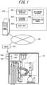
- FIG. 1 is an explanatory view illustrating a configuration of a partial discharge detection system.
- Electrical equipment 10 is equipment in which a switchboard, which transforms high voltage sent from an electric power company, is contained in a box.
- a detection sensor 100 which detects partial discharge
- a communication apparatus 190 which wirelessly communicates a detected signal
- the detection sensor 100 and the communication apparatus 190 correspond to a partial discharge detector.
- the detected signal is transmitted from the communication apparatus 190, through a relay 20, to an analyzer 200 via a network NE.
- the relay 20 is a device for connecting the communication apparatus 190 to the network NE, and various well-known devices can be used.
- the detection sensor 100 and the analyzer 200 can be connected in various ways, and the communication apparatus 190 and the analyzer 200 can be directly connected wirelessly or with wires. Both of the detection sensor 100 and the analyzer 200 may also be configured as a single unit.
- the detection sensor 100 can be mounted on the outside of the electrical equipment 10, as illustrated in solid lines in the figure, or on the inside of the electrical equipment 10, as illustrated in dashed lines.
- the communication apparatus 190A is also mounted on the inside.
- the communication apparatus 190A be configured to allow communication even when mounted on the inside of the electrical equipment 10. For example, a configuration to convey a detection signal to the communication apparatus 190 via electricity, light, or sound through the door of the electrical equipment 10 may be added.
- the analyzer 200 is built in software by installing a program that implements each of functions illustrated in the figure on a server. Some or all of the functions may be configured in hardware.
- a transmitter/receiver 201 performs the function of transmitting and receiving signals to and from the detection sensor 100 or the like via the network NE.
- a discharge detector 202 analyzes, based on a signal detected by the detection sensor 100, whether the signal corresponds to partial discharge.
- An alert unit 203 outputs an alert when the partial discharge is detected, and when it is determined that there is an abnormality in the switchboard.
- the alert can be output in various methods, for example, by transmitting an e-mail to a predetermined notification destination.
- a switchboard database 204 is a database that stores information on the switchboard, i.e., the electrical equipment 10. For example, information that identifies a switchboard, such as its location and name, is stored in correspondence with an identifier attached to the switchboard. This makes it possible to easily identify which switchboard a detection result is from, by receiving, from the detection sensor 100, the detection result together with the identifier.
- a detection log memory 205 stores past detection results for each switchboard. By storing the past detection results, for example, it is possible to check how often the partial discharge occurs and to analyze whether there is an abnormality in the switchboard.
- the partial discharge detection system is not limited to the configuration illustrated in FIG. 1 , but can take various configurations. Additional functions other than those illustrated may be added.
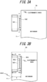
- FIGS. 2A and 2B are explanatory views illustrating the configuration of the detection sensor 100.
- FIG. 2A illustrates a perspective view.
- a housing of the detection sensor 100 is constituted of a main body 120 and a lid 140.
- an upper side of the housing in the figure is referred to as a front side and a lower side as a back side.
- an electrode 101 of a metal plate is affixed to a front surface of the electrode 101.
- a dielectric is affixed to a front surface of the electrode 101.
- the surface to which the electrode 101 is affixed is hereinafter referred to as a front surface, and the opposite side is referred to as a back surface.
- Magnets 107 with a length extending from the front surface to the back surface are embedded at four corners of the housing. With magnetic force of the magnets 107, the detection sensor 100 can be mounted on the electrical equipment 10 in either orientation on the front or back surface.
- the main body 120 of the housing is provided with a terminal 104 for outputting a detection signal.
- the terminal 104 and the electrode 101 are connected with a wire inside the main body 120.
- FIG. 2B illustrates the internal structure of the detection sensor 100 with the main body 120 and the lid 140 removed.
- a mounting portion 122 for mounting the terminal 104 is formed in a side surface 121 of the main body 120.
- the electrode and the terminal 104 are connected with a wire 105.
- Recessed portions 123 are provided at the four corners of the main body 120. Into each recessed portion 123, the cylindrical magnet 107 is inserted. In the lid 140, a mounting portion 142 for holding the terminal 104 is formed on a side surface 141. Convex portions 143 for holding the magnets 107 are formed at the four corners of the lid 140.
- the lid 140 holds the magnets 107 and terminal 104, as described above, so it is possible to easily configure the detection sensor 100 without using screws or other parts.
- the shape and structure of the detection sensor 100 are not limited to the example described above.
- the magnets 107 may be divided and mounted on the front and back surfaces.
- FIGS. 3A and 3B are explanatory views illustrating usage aspects of the detection sensor.
- FIG. 3A illustrates the detection sensor 100 mounted on the outside of the door 11 of the electrical equipment 10. At this time, the detection sensor 100 is mounted, by magnetic force F of the magnets 107, with the front surface facing the door 11. Since a dielectric 102 is affixed to the front surface of the electrode 101, by mounting the detection sensor 100 on the door 11, the dielectric 102 is sandwiched between the door 11 and the electrode 101.
- FIG. 3B illustrates the detection sensor 100 mounted on the inside of the door 11 of the electrical equipment 10.
- the detection sensor 100 is mounted, by magnetic force F1 of the magnets 107, with the back surface facing the door 11.
- an antenna plate 103 is mounted on the front surfaces of the electrode 101 and the dielectric 102 by magnetic force F2 of the magnets 107.
- the antenna plate 103 is a metal plate larger than the electrode 101.
- the electromagnetic waves are captured by the antenna plate 103 and detected by the detection sensor 100.
- the interposition of the dielectric 102 increases the capacitance of the electrode 101, which increases the detection sensitivity.
- the detection sensor 100 When the electrical equipment 10 is installed in noisy environment, noise is captured by the door 11 of the electrical equipment 10, as illustrated in the figure.
- the door 11 also performs the function of shielding the noise.
- the housing of the detection sensor 100 also performs the function of isolating the antenna plate 103, which captures the partial discharge, at a distance t from the door 11. Therefore, as illustrated in FIG. 3B , the detection sensor 100 according to the embodiment can detect the partial discharge with suppressing the influence of noise by being mounted on the inside of the door 11.
- the distance t from the door 11 to the antenna plate 103 (referred to as housing thickness t) can be determined arbitrarily, taking the influence of noise and other factors into consideration.
- FIG. 4 is a graph illustrating the influence of noise depending on the housing thickness. As illustrated in the figure, a noise contamination rate decreases monotonically as the housing thickness t increases. To sufficiently reduce noise, the housing thickness t is preferably set to 10 mm or more. However, since the increased housing thickness results in upsizing of the detection sensor 100, it is preferable to take this into consideration when determining the housing thickness.
- the dielectric 102 is affixed to the front surface of the electrode 101. This improves the detection sensitivity.
- FIG. 5 is a graph illustrating the relationship between the capacitance and the sensitivity.
- the vertical axis represents a sensitivity scaling based on the sensitivity of a conventional TEV sensor (coupling capacitance of the order of 11 pF).
- the sensitivity of the detection sensor 100 increases monotonically as the capacitance increases.
- the sensitivity of the detection sensor 100 does not increase linearly, but rather, in the range of the capacitance up to 204 pF, the sensitivity significantly increases to approximately 5 times by a slight increase in the capacitance, and in the range exceeding this, the influence by the increase in the capacitance becomes moderate and the sensitivity does not increase so significantly even when the capacitance increases. Therefore, in terms of obtaining sufficient sensitivity as the detection sensor 100, the capacitance is preferably set at approximately 200 pF or more.
- the dielectric 102 various materials can be used as the dielectric 102. In the embodiment, the following three materials are tested to select a material suitable for the detection sensor 100.
- FIGS. 6A and 6B are explanatory views illustrating the relationship between the material property and the capacitance of dielectrics.
- CS-3945 ® , ES-3346 ® , and AD-3396 ® are used in the embodiment.
- Characteristics, such as a relative dielectric constant and a sheet thickness, are illustrated in the table in FIG. 6A .
- FIG. 6B illustrates the capacitance in the case of using these materials.
- a curve A is the capacitance of the conventional TEV sensor. As illustrated in the figure, the capacitance is lowered in the order of CS-3945 ® , ES-3346 ® , and AD-3396 ® . It has been found that when CS-3945 ® is used, the capacitance exceeds 200 pF.
- the relative dielectric constant is increased in the order of CS-3945 ® , ES-3346 ® , and AD-3396 ® , but the material thickness becomes thinner in that order, so the overall capacitance of CS-3945 ® is the largest.
- both the relative dielectric constant and the thickness of the material concern with the capacitance.
- the example illustrated in the embodiment is just one example, and materials with various relative dielectric constants and material thicknesses can be selected.
- FIGS. 7A and 7B are explanatory views illustrating the configuration of the communication apparatus 190.
- FIG. 7A illustrates the schematic configuration of the communication apparatus 190.
- the communication apparatus 190 is provided with a conversion circuit 191, an AD converter 198, and a wireless communication unit 199.
- the conversion circuit 191 is a circuit for converting a high-frequency input signal into a low-frequency signal.
- the conversion circuit 191 includes a tuning circuit 192, a high-frequency amplification circuit 193, a detection circuit 194, and a low-frequency amplification circuit 195.
- FIG. 7B illustrates the specific circuit configuration.
- the tuning circuit 192 can be in tune with a wide range of frequencies by increasing the Q value.
- the circuit is designed to be in tune with 10 MHz to 20 MHz, as described below.
- an IC chip for amplitude modulation which constitutes the conversion circuit 191
- the conversion circuit can be thereby configured inexpensively and simply.
- the conversion circuit 191 is not limited to such a configuration, but various configurations that convert a high-frequency input signal into a low-frequency signal can be applied.
- the AD converter 198 converts the low-frequency output signal converted by the conversion circuit 191 into a digital signal.
- the wireless communication unit 199 wirelessly transmits the converted digital signal.
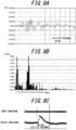
- FIGS. 8A to 8C are explanatory views illustrating the action of the conversion circuit 191.
- FIG. 8A illustrates an output signal from the detection sensor 100 when partial discharge is detected. As illustrated in the figure, the output signal has components of various frequencies.
- FIG. 8B illustrates the strength distribution of the output signal at each frequency.
- the output signal of the partial discharge has peaks of intensity at 10 MHz to 20 MHz and at 50 MHz to 100 MHz. Therefore, in order to detect the partial discharge with high accuracy, it is preferable to detect, by the tuning circuit 192, the frequencies of one or both of these two peaks.
- the circuit is configured to be in tune with 10 MHz to 20 MHz. This is because it is more efficient to convert a signal with lower frequencies of 10 MHz to 20 MHz to a low-frequency signal than to convert a signal with higher frequencies of 50 MHz to 100 MHz to a low-frequency signal. This is also because a tuning circuit for 10 MHz to 20 MHz can be realized at a lower cost.
- FIG. 8C illustrates an input waveform to and an output waveform from the conversion circuit 191.
- the detection signal due to the partial discharge has a very high-frequency pulsed waveform as illustrated in the input waveform in FIG. 8C , though contains various frequencies as illustrated in FIGS. 8A and 8B .
- this detection signal is converted into a low-frequency signal.
- the frequency after the conversion can be selected arbitrarily, but as an example, may be several tens of KHz, e.g., 50 KHz.
- the reason for converting into the low-frequency signal is as follows.
- Such a circuit is expensive, and the amount of data to be transmitted is also large, resulting in high power consumption.
- the embodiment avoids such issues by lowering the frequency, thus enabling the detection of the partial discharge at low cost and with low power consumption.
- the analyzer 200 detects whether the transmitted detection signal corresponds to the partial discharge.
- FIG. 9 is a flowchart of a discharge detection process. This is a process performed by the analyzer 200.
- the analyzer 200 receives a detection signal (step S10), and determines whether there is a discharge (step S11).
- a detection signal step S10
- determines whether there is a discharge step S11
- a method of determining the presence of the discharge is illustrated in the figure. As illustrated in the figure, as an example, it can be determined that there is a partial discharge when the strength of the detection signal exceeds a predetermined threshold value. The determination is not limited to such a method, but can be made by various other methods.
- step S12 When no partial discharge is detected (step S12), the discharge detection process ends.
- the analyzer 200 reads past detection logs (step S13), and outputs an alert (step S14) based on the determination of whether an alert is required. Whether the alert is required can be determined based on, for example, the number of detections of past partial discharge, the frequency of the detections, or the like. The alert can be output, for example, by sending an e-mail to a predetermined notification destination.
- the partial discharge occurring at high frequencies can be detected with high accuracy at low cost and with low power consumption.
- the partial discharge detector is mounted on the outside of the electrical equipment when used in environment with low noise, and on the inside of the electrical equipment when used in noisy environment, thus enabling the detection with suppressing the influence of noise.
- the partial discharge detector and the partial discharge detection system do not necessarily have to have all of the various features described in the embodiment, and may be configured by omitting or combining some of the features as appropriate.
- the present disclosure can be used to detect partial discharge that occurs in electrical equipment covering transformers or switchboards.
Landscapes
- Physics & Mathematics (AREA)
- General Physics & Mathematics (AREA)
- Engineering & Computer Science (AREA)
- Computer Networks & Wireless Communication (AREA)
- Testing Relating To Insulation (AREA)
Applications Claiming Priority (2)
| Application Number | Priority Date | Filing Date | Title |
|---|---|---|---|
| JP2022048110A JP7185966B1 (ja) | 2022-03-24 | 2022-03-24 | 部分放電検出装置 |
| PCT/JP2023/004874 WO2023181706A1 (ja) | 2022-03-24 | 2023-02-14 | 部分放電検出装置 |
Publications (2)
| Publication Number | Publication Date |
|---|---|
| EP4478065A1 true EP4478065A1 (de) | 2024-12-18 |
| EP4478065A4 EP4478065A4 (de) | 2025-05-28 |
Family
ID=84387540
Family Applications (1)
| Application Number | Title | Priority Date | Filing Date |
|---|---|---|---|
| EP23774305.9A Pending EP4478065A4 (de) | 2022-03-24 | 2023-02-14 | Teilentladungsdetektor |
Country Status (6)
| Country | Link |
|---|---|
| US (1) | US20250180624A1 (de) |
| EP (1) | EP4478065A4 (de) |
| JP (1) | JP7185966B1 (de) |
| KR (1) | KR20240137641A (de) |
| CN (1) | CN118742817A (de) |
| WO (1) | WO2023181706A1 (de) |
Families Citing this family (1)
| Publication number | Priority date | Publication date | Assignee | Title |
|---|---|---|---|---|
| WO2026006942A1 (zh) * | 2024-07-01 | 2026-01-08 | 上海华君智能科技有限公司 | 高频电磁波监测传感器及局放监测装置 |
Family Cites Families (11)
| Publication number | Priority date | Publication date | Assignee | Title |
|---|---|---|---|---|
| JPH0339670A (ja) * | 1989-07-06 | 1991-02-20 | Tokyo Electric Power Co Inc:The | 部分放電測定方法 |
| JPH0576122A (ja) * | 1991-09-11 | 1993-03-26 | Mitsubishi Electric Corp | 異常検出装置 |
| JPH09178803A (ja) * | 1995-12-26 | 1997-07-11 | Furukawa Electric Co Ltd:The | 電力ケーブルの部分放電測定方法 |
| JP4732192B2 (ja) * | 2006-02-28 | 2011-07-27 | 三菱電機株式会社 | Gis用部分放電検出センサおよびこれを使用する絶縁異常監視システム |
| JP2008304357A (ja) * | 2007-06-08 | 2008-12-18 | Mitsubishi Electric Corp | 部分放電計測装置 |
| JP6207462B2 (ja) * | 2014-05-26 | 2017-10-04 | 三菱電機株式会社 | 部分放電センサ |
| KR101456134B1 (ko) * | 2014-06-03 | 2014-11-04 | (주)한국이엔씨 | 아크와 코로나 발생에 따른 배전반(고압반, 저압반, 모터 제어반, 분전반)의 과도 대지 전압 검출 방법 |
| CN204575796U (zh) * | 2015-04-09 | 2015-08-19 | 国家电网公司 | 用于高压开关柜局部放电检测的tev传感器 |
| JP7127625B2 (ja) | 2019-08-06 | 2022-08-30 | Jfeスチール株式会社 | 部分放電検出装置および部分放電監視システム |
| CN110865284A (zh) * | 2019-11-12 | 2020-03-06 | 云南电网有限责任公司临沧供电局 | 一种基于聚偏二氟乙烯薄膜的磁吸式电容探头 |
| KR102192609B1 (ko) * | 2020-04-21 | 2020-12-17 | 주식회사 동일일렉트릭 | 순시유도전압센서를 이용한 부분방전 모니터링 감시기능이 탑재된 배전반(고압 배전반, 저압 배전반, 분전반, 모터제어반) |
-
2022
- 2022-03-24 JP JP2022048110A patent/JP7185966B1/ja active Active
-
2023
- 2023-02-14 CN CN202380023465.6A patent/CN118742817A/zh active Pending
- 2023-02-14 EP EP23774305.9A patent/EP4478065A4/de active Pending
- 2023-02-14 KR KR1020247027806A patent/KR20240137641A/ko active Pending
- 2023-02-14 WO PCT/JP2023/004874 patent/WO2023181706A1/ja not_active Ceased
- 2023-02-14 US US18/843,812 patent/US20250180624A1/en active Pending
Also Published As
| Publication number | Publication date |
|---|---|
| JP2023141670A (ja) | 2023-10-05 |
| US20250180624A1 (en) | 2025-06-05 |
| KR20240137641A (ko) | 2024-09-20 |
| JP7185966B1 (ja) | 2022-12-08 |
| EP4478065A4 (de) | 2025-05-28 |
| WO2023181706A1 (ja) | 2023-09-28 |
| CN118742817A (zh) | 2024-10-01 |
Similar Documents
| Publication | Publication Date | Title |
|---|---|---|
| EP3143416B1 (de) | Teilentladungserfassungssystem mit elektrischem feldsensor mit kapazitiver kopplung | |
| US8392134B2 (en) | Antenna testing device and antenna testing method using the same | |
| KR101113193B1 (ko) | 부분방전검출센서, 부분방전검출장치 및부분방전검출센서를 가지는 가스절연 전기기기 | |
| CN107407708A (zh) | 局部放电检测系统 | |
| CN108710074A (zh) | 一种基于无线传输技术的开关柜局部放电检测系统 | |
| GB2474125A (en) | Partial discharge detector for gas insulated electric apparatus | |
| EP4478065A1 (de) | Teilentladungsdetektor | |
| CN101044410B (zh) | 旋转电机的局部放电检测装置和检测方法 | |
| WO1997009627A1 (en) | Electric field measurement system | |
| CN105738786A (zh) | 一种屏蔽外界干扰的gis超高频局部放电信号采集装置 | |
| KR101005230B1 (ko) | 가스절연개폐장치의 부분방전신호 검출용 신호변환장치 및 그를 이용한 부분방전 검출 시스템 | |
| CN114047374B (zh) | 一种gis手窗式vfto传感与触发一体化测量装置 | |
| US7930940B2 (en) | Ultrasonic transducer | |
| CN117723903A (zh) | 一种局部放电检测装置及系统 | |
| JP2000346901A (ja) | 電気機器の部分放電検出装置及び検出器 | |
| US9410997B2 (en) | Crystal unit and method of measuring characteristics of the crystal unit | |
| JP4279517B2 (ja) | アンテナ特性測定方法 | |
| EP4134689A1 (de) | Elektromagnetischer feldsensor | |
| CN120651376B (zh) | 一种gis母线电连接区域温度监测装置及其监测方法 | |
| JP7475740B1 (ja) | 部分放電検出システム | |
| JPH11211760A (ja) | ピーク検出器、並びにそれを用いた高電圧機器の絶縁監視装置及びシステム | |
| CN111800717A (zh) | 一种抗射频干扰电路及驻极体麦克风 | |
| JP2006329636A (ja) | 部分放電検出装置および部分放電試験方法 | |
| CN107271935A (zh) | 一种磁共振耦合空间高频磁场强度测量装置和方法 | |
| JPH1130636A (ja) | 高周波電流測定器 |
Legal Events
| Date | Code | Title | Description |
|---|---|---|---|
| STAA | Information on the status of an ep patent application or granted ep patent |
Free format text: STATUS: THE INTERNATIONAL PUBLICATION HAS BEEN MADE |
|
| PUAI | Public reference made under article 153(3) epc to a published international application that has entered the european phase |
Free format text: ORIGINAL CODE: 0009012 |
|
| STAA | Information on the status of an ep patent application or granted ep patent |
Free format text: STATUS: REQUEST FOR EXAMINATION WAS MADE |
|
| 17P | Request for examination filed |
Effective date: 20240912 |
|
| AK | Designated contracting states |
Kind code of ref document: A1 Designated state(s): AL AT BE BG CH CY CZ DE DK EE ES FI FR GB GR HR HU IE IS IT LI LT LU LV MC ME MK MT NL NO PL PT RO RS SE SI SK SM TR |
|
| A4 | Supplementary search report drawn up and despatched |
Effective date: 20250428 |
|
| RIC1 | Information provided on ipc code assigned before grant |
Ipc: G01R 31/12 20200101AFI20250422BHEP |
|
| DAV | Request for validation of the european patent (deleted) | ||
| DAX | Request for extension of the european patent (deleted) |