EP4478599A1 - Procédé de surmodulation d'un onduleur multiphase, produit de programme informatique et onduleur multiphase - Google Patents
Procédé de surmodulation d'un onduleur multiphase, produit de programme informatique et onduleur multiphase Download PDFInfo
- Publication number
- EP4478599A1 EP4478599A1 EP23216742.9A EP23216742A EP4478599A1 EP 4478599 A1 EP4478599 A1 EP 4478599A1 EP 23216742 A EP23216742 A EP 23216742A EP 4478599 A1 EP4478599 A1 EP 4478599A1
- Authority
- EP
- European Patent Office
- Prior art keywords
- inverter
- angle
- phase
- phase inverter
- voltage
- Prior art date
- Legal status (The legal status is an assumption and is not a legal conclusion. Google has not performed a legal analysis and makes no representation as to the accuracy of the status listed.)
- Pending
Links
Images

Classifications
-
- H—ELECTRICITY
- H02—GENERATION; CONVERSION OR DISTRIBUTION OF ELECTRIC POWER
- H02M—APPARATUS FOR CONVERSION BETWEEN AC AND AC, BETWEEN AC AND DC, OR BETWEEN DC AND DC, AND FOR USE WITH MAINS OR SIMILAR POWER SUPPLY SYSTEMS; CONVERSION OF DC OR AC INPUT POWER INTO SURGE OUTPUT POWER; CONTROL OR REGULATION THEREOF
- H02M7/00—Conversion of AC power input into DC power output; Conversion of DC power input into AC power output
- H02M7/42—Conversion of DC power input into AC power output without possibility of reversal
- H02M7/44—Conversion of DC power input into AC power output without possibility of reversal by static converters
- H02M7/48—Conversion of DC power input into AC power output without possibility of reversal by static converters using discharge tubes with control electrode or semiconductor devices with control electrode
- H02M7/53—Conversion of DC power input into AC power output without possibility of reversal by static converters using discharge tubes with control electrode or semiconductor devices with control electrode using devices of a triode or transistor type requiring continuous application of a control signal
- H02M7/537—Conversion of DC power input into AC power output without possibility of reversal by static converters using discharge tubes with control electrode or semiconductor devices with control electrode using devices of a triode or transistor type requiring continuous application of a control signal using semiconductor devices only, e.g. single switched pulse inverters
- H02M7/5387—Conversion of DC power input into AC power output without possibility of reversal by static converters using discharge tubes with control electrode or semiconductor devices with control electrode using devices of a triode or transistor type requiring continuous application of a control signal using semiconductor devices only, e.g. single switched pulse inverters in a bridge configuration
- H02M7/53871—Conversion of DC power input into AC power output without possibility of reversal by static converters using discharge tubes with control electrode or semiconductor devices with control electrode using devices of a triode or transistor type requiring continuous application of a control signal using semiconductor devices only, e.g. single switched pulse inverters in a bridge configuration with automatic control of output voltage or current
- H02M7/53875—Conversion of DC power input into AC power output without possibility of reversal by static converters using discharge tubes with control electrode or semiconductor devices with control electrode using devices of a triode or transistor type requiring continuous application of a control signal using semiconductor devices only, e.g. single switched pulse inverters in a bridge configuration with automatic control of output voltage or current with analogue control of three-phase output
-
- H—ELECTRICITY
- H02—GENERATION; CONVERSION OR DISTRIBUTION OF ELECTRIC POWER
- H02P—CONTROL OR REGULATION OF ELECTRIC MOTORS, ELECTRIC GENERATORS OR DYNAMO-ELECTRIC CONVERTERS; CONTROLLING TRANSFORMERS, REACTORS OR CHOKE COILS
- H02P27/00—Arrangements or methods for the control of AC motors characterised by the kind of supply voltage
- H02P27/04—Arrangements or methods for the control of AC motors characterised by the kind of supply voltage using variable-frequency supply voltage, e.g. inverter or converter supply voltage
- H02P27/06—Arrangements or methods for the control of AC motors characterised by the kind of supply voltage using variable-frequency supply voltage, e.g. inverter or converter supply voltage using DC to AC converters or inverters
- H02P27/08—Arrangements or methods for the control of AC motors characterised by the kind of supply voltage using variable-frequency supply voltage, e.g. inverter or converter supply voltage using DC to AC converters or inverters with pulse width modulation
-
- H—ELECTRICITY
- H02—GENERATION; CONVERSION OR DISTRIBUTION OF ELECTRIC POWER
- H02M—APPARATUS FOR CONVERSION BETWEEN AC AND AC, BETWEEN AC AND DC, OR BETWEEN DC AND DC, AND FOR USE WITH MAINS OR SIMILAR POWER SUPPLY SYSTEMS; CONVERSION OF DC OR AC INPUT POWER INTO SURGE OUTPUT POWER; CONTROL OR REGULATION THEREOF
- H02M7/00—Conversion of AC power input into DC power output; Conversion of DC power input into AC power output
- H02M7/42—Conversion of DC power input into AC power output without possibility of reversal
- H02M7/44—Conversion of DC power input into AC power output without possibility of reversal by static converters
- H02M7/48—Conversion of DC power input into AC power output without possibility of reversal by static converters using discharge tubes with control electrode or semiconductor devices with control electrode
- H02M7/53—Conversion of DC power input into AC power output without possibility of reversal by static converters using discharge tubes with control electrode or semiconductor devices with control electrode using devices of a triode or transistor type requiring continuous application of a control signal
- H02M7/537—Conversion of DC power input into AC power output without possibility of reversal by static converters using discharge tubes with control electrode or semiconductor devices with control electrode using devices of a triode or transistor type requiring continuous application of a control signal using semiconductor devices only, e.g. single switched pulse inverters
- H02M7/5387—Conversion of DC power input into AC power output without possibility of reversal by static converters using discharge tubes with control electrode or semiconductor devices with control electrode using devices of a triode or transistor type requiring continuous application of a control signal using semiconductor devices only, e.g. single switched pulse inverters in a bridge configuration
- H02M7/53871—Conversion of DC power input into AC power output without possibility of reversal by static converters using discharge tubes with control electrode or semiconductor devices with control electrode using devices of a triode or transistor type requiring continuous application of a control signal using semiconductor devices only, e.g. single switched pulse inverters in a bridge configuration with automatic control of output voltage or current
- H02M7/53875—Conversion of DC power input into AC power output without possibility of reversal by static converters using discharge tubes with control electrode or semiconductor devices with control electrode using devices of a triode or transistor type requiring continuous application of a control signal using semiconductor devices only, e.g. single switched pulse inverters in a bridge configuration with automatic control of output voltage or current with analogue control of three-phase output
- H02M7/53876—Conversion of DC power input into AC power output without possibility of reversal by static converters using discharge tubes with control electrode or semiconductor devices with control electrode using devices of a triode or transistor type requiring continuous application of a control signal using semiconductor devices only, e.g. single switched pulse inverters in a bridge configuration with automatic control of output voltage or current with analogue control of three-phase output based on synthesising a desired voltage vector via the selection of appropriate fundamental voltage vectors, and corresponding dwelling times
Definitions
- the invention relates to a method for overmodulating a multi-phase inverter, a computer program product, and a multi-phase inverter.
- Pulse Width Modulation may be used for the convert alternating current (AC) waveforms from DC power.
- Inverters that make use of PWM can drive 3 phase AC powered motors at varying speeds from DC, in particular using multiple class-D amplifiers.
- EP 1 525 655 B1 discloses a drive system for a three-phase brushless AC motor that is arranged to optimize the transistor switching pattern to improve power output whilst allowing current measurement in all of the phases using a single sensor.
- DE 10 2007 012 350 A1 relates to PWM methods and an apparatus that are provided for loss-minimized control of AC motors.
- the method includes providing a voltage to the AC motor based on a switching cycle, adding a duty cycle of a zero vector to each phase leg of the switching cycle when a duty cycle of a first phase leg of the switching cycle is less than a minimum duty cycle, and subtracting the duty cycle of the zero vector from each phase leg of the switching cycle when a second duty cycle of a second phase leg is greater than a maximum duty cycle.
- a method for overmodulating a multi-phase inverter that is configured to convert a DC input voltage to an AC output voltage comprising:
- a process for determining an optimized overmodulation scheme for an inverter comprises obtaining at least one hardware constraint of the inverter as well as determining a hold and a clamp angle, wherein the hold angle is an angle or angle range in which the duty cycle of the inverter is kept at a constant level, wherein the clamp angle is an angle or angle range in which the voltage is clamped at a maximum level, and wherein the determination of the angles is based on an algorithm which uses the hardware constraint as an input parameter.
- a multi-phase inverter also known as a multi-leg inverter, may be considered as an electronic device that converts DC (direct current) power into AC (alternating current) power in a multi-phase electrical system.
- the multi-phase inverter may comprise multiple, in particular three legs, wherein the legs are responsible for generating one phase of the AC output waveform.
- the multi-phase inverter may be configured to be used at least in a motor drive, in particular of an electric vehicle, a renewable energy system, or a power conversion device.
- the multi-phase inverter may comprise a set of power switching devices, such as insulated-gate bipolar transistors (IGBTs) or metal-oxide-semiconductor field-effect transistors (MOSFETs), which are controlled by a modulation technique, such as pulse width modulation (PWM).
- IGBTs insulated-gate bipolar transistors
- MOSFETs metal-oxide-semiconductor field-effect transistors
- PWM pulse width modulation
- the multi-phase inverter receives a DC power input and, through the controlled switching of the power devices, produces a multi-phase AC output with adjustable voltage magnitude, frequency, and waveform shape.
- the control of the switching devices is achieved by employing the modulation strategy to generate the desired AC output waveform.
- Determining at least one hardware limitation may comprise at least one of a measurement of a hardware limitation, obtaining data from a database, in particular over the internet, or a user input.
- the calculating may be considered as a process of determining an output value based on at least one input value.
- the calculation may include an algorithm.
- a hold angle may be an angle of at least one phase of the inverter or a range of angles of at least one phase of the inverter, for which a duty cycle of the inverter is kept at a constant level.
- a clamp angle may be an angle of at least one phase of the inverter or a range of angles of at least one phase of the inverter, for which the AC output voltage is clamped to one half of the DC input voltage, in particular by the calculation unit. This one half of the DC input voltage may correspond to the maximum achievable AC output voltage.
- Calculating the hold angle and/or the clamp angle is specific for the at least one hardware limitation of the inverter.
- the hardware limitation that is used for the calculation at least partially determines the value or values for the hold angle and/or the clamp angle.
- At least a clamping duty cycle or modulation index may be calculated.
- the method for overmodulating a multi-phase inverter provides a way to obtain an accurate output voltage, in particular at high modulation index values.
- the determination of the at least one hardware limitation of the multi-phase inverter provides information that can be used in the calculation steps. Calculating the hold angle and the clamp angle allows defining a scheme for the overmodulation, which can be immediately used for driving the inverter accordingly.
- the hold angle and/or the clamp angle are specific for the at least one hardware limitation of the inverter, the knowledge of the limitations of the components of the inverter can be used in order to obtain an optimized overmodulation in terms of accuracy.
- a method according to the invention may advantageously provide that the constant level is the maximum duty cycle of the inverter.
- the maximum duty cycle may be a result of a hardware limitation of the switches used and/or of the control of the switches. When the maximum duty cycle of the inverter is used for the constant level, the maximum of energy providable by the inverter may be obtained.
- the hardware limitation is at least one of the maximum duty cycle of the multi-phase inverter, a modulation index of the inverter, a setpoint for the modulation index of the inverter, or a dead time of the inverter.
- the maximum duty cycle refers to the highest allowable value for the duty cycle of the pulse width modulation (PWM) signals used to control the switching in the inverter.
- the duty cycle represents the ratio of an ON-time (time during which the power device is conducting) to the total period of the PWM signal. It may be expressed as a percentage.
- the maximum duty cycle value can be determined by various factors, including the design of the inverter, the specifications of the switches (such as IGBTs or MOSFETs), and the desired operating parameters. It is typically set to ensure safe and reliable operation of the power devices and to avoid exceeding their maximum ratings.
- the modulation index of an inverter may be a parameter that quantifies the level of modulation applied to the pulse width modulation (PWM) signals used to control the switching of the switches in the inverter.
- PWM pulse width modulation
- the modulation index may be defined as the ratio between the peak amplitude of the modulating signal and the peak amplitude of the carrier signal in the PWM scheme. It may represent the extent to which the carrier signal is modulated to generate the desired output waveform.
- the modulation index may determine the relationship between the amplitude of the AC output voltage and the reference voltage or command signal. Thus, adjusting the modulation index may control the output voltage magnitude.
- a modulation index of 1 may indicate a full modulation, where the amplitude of the carrier signal is modulated between zero and the peak value of the reference signal. Lower modulation indices result in reduced output voltage magnitudes, while higher modulation indices lead to larger output voltage magnitudes.
- the setpoint for the modulation index of the inverter may be regarded as a value that is set by a user and/or determined by the application.
- the dead time of the inverter may refer to a time period during which both the upper and lower switches (also known as power devices) of one of the legs are intentionally turned off. This dead time may be introduced to prevent cross-conduction or shoot-through current between the switches.
- a time gap is inserted between turning off one switch and turning on the other switch. This ensures that both switches are not conducting simultaneously, effectively avoiding the cross-conduction condition.
- the dead time allows for the proper commutation of the power devices and reduces the likelihood of short circuits or excessive currents during the switching process.
- the duration of the dead time may be in the order of microseconds.
- the dead time may be determined by at least one of the characteristics of the power devices, the switching speed, and the voltage or current requirements of the application.
- calculating the hold angle and/or the clamp angle is provided by a search algorithm, in particular wherein the search algorithm considers at least a voltage accuracy, a total harmonic distortion or a phase accuracy.
- a search algorithm is a computational method or procedure used to systematically explore a problem space in order to find an optimal solution or make informed decisions. It is a systematic approach to solving problems by iteratively examining different possibilities or configurations.
- a search algorithm can be employed in a method according to the invention that is configured to explore and evaluate various overmodulation strategies, in particular different combinations of hold and/or clamp angles to find the optimal scheme that meets specific criteria or objectives (in particular a voltage accuracy, a total harmonic distortion or a phase accuracy).
- a search algorithm provides that advantage that it can explore a large solution space in a relatively short amount it time.
- specific optimization objectives such as maximizing output voltage magnitude, minimizing harmonic distortion, or improving energy efficiency
- a search algorithm can evaluate different schemes and guide the search towards finding the scheme that best satisfies these objectives.
- constraints and trade-offs may be considered. Inverter systems all have specific constraints, such as limitations on available resources, component specifications, or operating conditions.
- a search algorithm can take these constraints into account and help identify the scheme that optimizes performance while adhering to the given constraints. It can also help in exploring trade-offs between different performance metrics and finding a balanced solution.
- the search strategy is configured to solve a constraint satisfaction problem, wherein in particular the constraint to be satisfied is at least one of voltage accuracy, a total harmonic distortion or a phase accuracy.
- a constraint satisfaction problem may be regarded as a computational problem that involves finding a solution that satisfies a set of constraints and/or conditions.
- the problem is defined by a set of variables, each with a domain of possible values, and a set of constraints that restrict the combinations of values that the variables can take.
- using a CSP formulation offers the advantage of leveraging the defined constraints to efficiently prune the search space, handle the complex relationships, and support incremental refinement. These advantages enhance the search for an optimized overmodulation scheme, enabling the identification of hold and clamp angles that result at least in a high voltage accuracy, a low total harmonic distortion or a high phase accuracy.
- an output is generated, which includes at least one of the hold angle, the clamp angle, a voltage gain factor, or a scaling duty cycle.
- the hold angle, the clamp angle, a voltage gain factor, or a scaling duty cycle may be provided as data or a data set, which can be in particular provided via an interface. This provides the advantage that the overmodulation scheme can be considered by other components, in particular the load driven by the inverter.
- a computer program product comprising instructions which, when the program is executed by a computer, cause the computer to carry out a method according to the invention.
- a multi-phase inverter configured to perform an inventive method.
- a multi-phase inverter brings the same advantages as have already been described in detail with reference to a method according to the invention and/or a computer program product according to the invention.
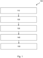
- Figure 1 shows a method 100 for overmodulating a multi-phase inverter that is configured to convert a DC input voltage to an AC output voltage, comprising:
- the method 100 for overmodulating a multi-phase inverter provides a way to obtain an accurate output voltage, in particular at high modulation index values.
- the determination of the at least one hardware limitation of the multi-phase inverter provides information that can be used in the calculation steps.
- Calculating 110, 120 the hold angle 210 and the clamp angle 220 allows defining a scheme for the overmodulation, which can be immediately used for driving the inverter accordingly.
- the hold angle 210 and/or the clamp angle 220 are specific for the at least one hardware limitation of the inverter, the knowledge of the limitations of the components of the inverter can be used in order to obtain an optimized overmodulation in terms of accuracy.
- a method 100 can comprise a switching 140 at least three half bridges of the inverter for converting the DC input voltage to the AC output voltage, wherein the at least three half bridges are switched according to the calculated 120, 130 hold angle 210 and/or clamp angle 220.
- the actual switching of the switches in the half bridges may be part of the method 100.
- an output is generated 150, which includes at least one of the hold angle 210, the clamp angle 220, a voltage gain factor, or a scaling duty cycle.
- the hold angle 210, the clamp angle 220, a voltage gain factor, or a scaling duty cycle may be provided as data or a data set, which can be in particular provided via an interface. This provides the advantage that the overmodulation scheme can be considered by other components, in particular the load driven by the inverter.
- Figure 2 shows an example of a possible duty cycle (on the y-axis) of one phase as a function of the phase angle (on the x-axis) within the overmodulation scheme obtained by a method according to the invention.
- the dashed line represents a second phase.
- the duty cycle is constant for the hold angle 210 and clamped to the maximum duty cycle for the determined clamp angle 220.
Landscapes
- Engineering & Computer Science (AREA)
- Power Engineering (AREA)
- Inverter Devices (AREA)
Applications Claiming Priority (1)
| Application Number | Priority Date | Filing Date | Title |
|---|---|---|---|
| DE102023115622 | 2023-06-15 |
Publications (1)
| Publication Number | Publication Date |
|---|---|
| EP4478599A1 true EP4478599A1 (fr) | 2024-12-18 |
Family
ID=89222881
Family Applications (1)
| Application Number | Title | Priority Date | Filing Date |
|---|---|---|---|
| EP23216742.9A Pending EP4478599A1 (fr) | 2023-06-15 | 2023-12-14 | Procédé de surmodulation d'un onduleur multiphase, produit de programme informatique et onduleur multiphase |
Country Status (1)
| Country | Link |
|---|---|
| EP (1) | EP4478599A1 (fr) |
Citations (3)
| Publication number | Priority date | Publication date | Assignee | Title |
|---|---|---|---|---|
| DE102007012350A1 (de) | 2006-03-16 | 2007-10-18 | GM Global Technology Operations, Inc., Detroit | Verfahren und Vorrichtung zur PWM-Steuerung eines Spannungszwischenkreisumrichters |
| EP1525655B1 (fr) | 2002-06-07 | 2018-02-28 | TRW Limited | Commande de moteur comprenant un seul detecteur de courant et utilisant une technique de vecteur spatial |
| US20190097562A1 (en) * | 2017-09-22 | 2019-03-28 | GM Global Technology Operations LLC | Quasi six-step pwm control |
-
2023
- 2023-12-14 EP EP23216742.9A patent/EP4478599A1/fr active Pending
Patent Citations (3)
| Publication number | Priority date | Publication date | Assignee | Title |
|---|---|---|---|---|
| EP1525655B1 (fr) | 2002-06-07 | 2018-02-28 | TRW Limited | Commande de moteur comprenant un seul detecteur de courant et utilisant une technique de vecteur spatial |
| DE102007012350A1 (de) | 2006-03-16 | 2007-10-18 | GM Global Technology Operations, Inc., Detroit | Verfahren und Vorrichtung zur PWM-Steuerung eines Spannungszwischenkreisumrichters |
| US20190097562A1 (en) * | 2017-09-22 | 2019-03-28 | GM Global Technology Operations LLC | Quasi six-step pwm control |
Non-Patent Citations (2)
| Title |
|---|
| BRIAN A WELCHKO ET AL: "Effects and Compensation of Dead-Time and Minimum Pulse-Width Limitations in Two-Level PWM Voltage Source Inverters", THE 2006 IEEE INDUSTRY APPLICATIONS CONFERENCE FORTY-FIRST IAS ANNUAL MEETING, CONFERENCE RECORD OF, IEEE, PISCATAWAY, NJ, US, 1 October 2006 (2006-10-01), pages 889 - 896, XP031026133, ISBN: 978-1-4244-0364-6 * |
| KAURA V: "A new method to linearize any triangle comparison based PWM by reshaping the modulation command", CONFERENCE RECORD OF THE 1996 IEEE INDUSTRY APPLICATIONS CONFERENCE - 31ST IAS ANNUAL MEETING, IEEE SERVICE CENTER, US, vol. 2, 6 October 1996 (1996-10-06), pages 927 - 933, XP010201408, ISBN: 978-0-7803-3544-8, DOI: 10.1109/IAS.1996.560194 * |
Similar Documents
| Publication | Publication Date | Title |
|---|---|---|
| CN110323991B (zh) | 向多相负载提供多相电流的功率模块和方法 | |
| US6023417A (en) | Generalized discontinuous pulse width modulator | |
| Gulbudak et al. | FPGA-based model predictive controller for direct matrix converter | |
| Kouro et al. | High-performance torque and flux control for multilevel inverter fed induction motors | |
| US7881081B1 (en) | Systems and methods for reducing AC drive common-mode currents | |
| EP0410463B1 (fr) | Système de convertisseur/onduleur du type tension à modulation de largeur d'impulsion et sa méthode de régulation | |
| CN108123653B (zh) | 马达控制系统的自适应脉宽调制 | |
| US8030874B2 (en) | Power converting apparatus | |
| CN101375488A (zh) | 用于控制电压源逆变器的电压线性的方法和设备 | |
| WO2004036755A9 (fr) | Modulateur a modulation d'impulsions en duree a vecteur spatial pour moteur a aimant permanent | |
| KR20160122923A (ko) | 3상 인버터의 옵셋 전압 생성 장치 및 방법 | |
| US11557998B2 (en) | Open loop duty control with automatic field orientation for a permanent magnet AC (PMAC) motor | |
| CN106026724A (zh) | 用于电力逆变器的控制装置 | |
| JPH07227085A (ja) | 電力変換装置 | |
| US11218085B2 (en) | Power conversion device having an inverter circuit including current limitation circuits and a control circuit controlling same | |
| EP4478599A1 (fr) | Procédé de surmodulation d'un onduleur multiphase, produit de programme informatique et onduleur multiphase | |
| US11646676B2 (en) | Method and apparatus for generating a three-phase voltage | |
| Neubert et al. | Performance comparison of inverter and drive configurations with open-end and star-connected windings | |
| WO2018179234A1 (fr) | Convertisseur en pont h et conditionneur d'énergie | |
| EP4195494A1 (fr) | Affaiblissement de flux adaptatif de charge d'un moteur synchrone à aimant permanent fonctionnant en mode de commande de tension | |
| Zhou et al. | Active vector modification for circulating current suppression of paralleled inverters using two-step sector indexing-based discontinuous SVPWM | |
| CN104685780A (zh) | 在变流器中的电流过零 | |
| US6246208B1 (en) | Method of feeding asynchronous motors with an inverter, in particular for battery-powered vehicles | |
| US11705848B2 (en) | Method for actuating an electrical circuit arrangement comprising at least one switching element, a control unit, an electrical circuit device, and a motor vehicle | |
| KR20170015946A (ko) | 유도 전동기 구동용 전압보상장치 및 이를 이용한 전압보상방법 |
Legal Events
| Date | Code | Title | Description |
|---|---|---|---|
| PUAI | Public reference made under article 153(3) epc to a published international application that has entered the european phase |
Free format text: ORIGINAL CODE: 0009012 |
|
| STAA | Information on the status of an ep patent application or granted ep patent |
Free format text: STATUS: THE APPLICATION HAS BEEN PUBLISHED |
|
| AK | Designated contracting states |
Kind code of ref document: A1 Designated state(s): AL AT BE BG CH CY CZ DE DK EE ES FI FR GB GR HR HU IE IS IT LI LT LU LV MC ME MK MT NL NO PL PT RO RS SE SI SK SM TR |
|
| STAA | Information on the status of an ep patent application or granted ep patent |
Free format text: STATUS: REQUEST FOR EXAMINATION WAS MADE |
|
| 17P | Request for examination filed |
Effective date: 20250513 |