EP4481411A1 - Dispositif et procédé de surveillance d'une capacité de coupure - Google Patents
Dispositif et procédé de surveillance d'une capacité de coupure Download PDFInfo
- Publication number
- EP4481411A1 EP4481411A1 EP24183030.6A EP24183030A EP4481411A1 EP 4481411 A1 EP4481411 A1 EP 4481411A1 EP 24183030 A EP24183030 A EP 24183030A EP 4481411 A1 EP4481411 A1 EP 4481411A1
- Authority
- EP
- European Patent Office
- Prior art keywords
- actuating element
- capacitance
- voltage
- actuating
- electrical
- Prior art date
- Legal status (The legal status is an assumption and is not a legal conclusion. Google has not performed a legal analysis and makes no representation as to the accuracy of the status listed.)
- Pending
Links
Images

Classifications
-
- H—ELECTRICITY
- H03—ELECTRONIC CIRCUITRY
- H03K—PULSE TECHNIQUE
- H03K17/00—Electronic switching or gating, i.e. not by contact-making and –breaking
- H03K17/18—Modifications for indicating state of switch
-
- G—PHYSICS
- G01—MEASURING; TESTING
- G01R—MEASURING ELECTRIC VARIABLES; MEASURING MAGNETIC VARIABLES
- G01R31/00—Arrangements for testing electric properties; Arrangements for locating electric faults; Arrangements for electrical testing characterised by what is being tested not provided for elsewhere
- G01R31/26—Testing of individual semiconductor devices
- G01R31/2607—Circuits therefor
- G01R31/2621—Circuits therefor for testing field effect transistors, i.e. FET's
-
- G—PHYSICS
- G01—MEASURING; TESTING
- G01R—MEASURING ELECTRIC VARIABLES; MEASURING MAGNETIC VARIABLES
- G01R31/00—Arrangements for testing electric properties; Arrangements for locating electric faults; Arrangements for electrical testing characterised by what is being tested not provided for elsewhere
-
- G—PHYSICS
- G01—MEASURING; TESTING
- G01R—MEASURING ELECTRIC VARIABLES; MEASURING MAGNETIC VARIABLES
- G01R15/00—Details of measuring arrangements of the types provided for in groups G01R17/00 - G01R29/00, G01R33/00 - G01R33/26 or G01R35/00
- G01R15/04—Voltage dividers
-
- G—PHYSICS
- G01—MEASURING; TESTING
- G01R—MEASURING ELECTRIC VARIABLES; MEASURING MAGNETIC VARIABLES
- G01R19/00—Arrangements for measuring currents or voltages or for indicating presence or sign thereof
- G01R19/0023—Measuring currents or voltages from sources with high internal resistance by means of measuring circuits with high input impedance, e.g. OP-amplifiers
-
- G—PHYSICS
- G01—MEASURING; TESTING
- G01R—MEASURING ELECTRIC VARIABLES; MEASURING MAGNETIC VARIABLES
- G01R19/00—Arrangements for measuring currents or voltages or for indicating presence or sign thereof
- G01R19/25—Arrangements for measuring currents or voltages or for indicating presence or sign thereof using digital measurement techniques
-
- G—PHYSICS
- G01—MEASURING; TESTING
- G01R—MEASURING ELECTRIC VARIABLES; MEASURING MAGNETIC VARIABLES
- G01R31/00—Arrangements for testing electric properties; Arrangements for locating electric faults; Arrangements for electrical testing characterised by what is being tested not provided for elsewhere
- G01R31/327—Testing of circuit interrupters, switches or circuit-breakers
Definitions
- the present disclosure relates to a device for monitoring a switch-off capability of a consumer, in particular by means of a switching element.
- the disclosure further relates to methods for monitoring a switch-off capability, as well as a control device, a system and a computer program.
- a typical challenge with such devices can be to be able to diagnose the ability of a digital output to turn off when it is switched on, especially when a load is connected.
- a safety function should be provided with a very high degree of probability in accordance with its specification to protect against injuries to third parties, irreversible damage and accidents resulting in death. It should be possible to ensure that safe digital outputs can be switched off with a high degree of probability.
- Cyclic switching can be carried out, for example in a time range of 1 ms to every 500 ms. Cyclic switching can be disruptive to the function of the switching elements in practical applications. In this respect, it may be necessary to diagnose the ability to switch off and to ensure it with a high degree of probability without having to switch off.
- the US 2012/0161817 A1 describes a circuit to supply a coil of a relay with electrical power.
- the current required for this can be provided by a battery.
- Two parallel supply lines are provided, each of which has a field effect transistor as a switch.
- the gate voltages of the field effect transistors are synchronously brought to a value at which current flows through both field effect transistors.
- the gate voltage is slightly reduced and the voltage drop between drain and source is measured.
- the measured values are evaluated for a wire break in the supply line to the field effect transistor.
- a disadvantage can be that the junction capacitance is not measured, but the FET is only cyclically controlled with a lower voltage. In addition, the load voltage must be measured. No measurement system with high reliability is shown.
- the EP 133 5471 A2 and the DE 382 1065 show a protective circuit using a "monitor" transistor.
- the main transistor is switched off if the voltage across it is too high.
- the disadvantage here can be that the main transistor is only protected if the voltage across it is too high, but not if it has become faultily low-resistance and can therefore no longer be switched off.
- the object of the present disclosure is to provide a device and a method which are each suitable for at least partially overcoming the aforementioned disadvantages of the prior art and for enriching the prior art.
- the operating state of the second actuating element is characterized by a second electrical quantity, which is a second capacitance on the second actuating element, and a second voltage.
- the first capacitance and the second capacitance are connected in series.
- a control device is provided which is designed to control the second actuating element by means of the second actuating signal at least in measuring intervals spaced apart from one another in time and to evaluate values of the first electrical quantity obtained in this way to detect a malfunction for switching off the first actuating element, and wherein the evaluation includes a comparison of the values of the first electrical quantity obtained with at least one reference default value.
- capacitance can be understood as an electrical quantity with the ability to store an electrical charge and build up a capacitance.
- a capacitance can be built up by applying a voltage.
- turn-off capability may be understood as the ability of an actuating element, for example a field effect transistor (FET), in which a current flow between source and drain can be completely interrupted when a suitable control voltage is applied to the gate.
- FET field effect transistor
- the turn-off capability may occur when the voltage at the gate is adjusted such that the electric field in the channel is strong enough to completely block the current flow. In this state, the FET is considered to be "turned off” and only a very small leakage current flows between source and drain.
- the ratio between the leakage current in the off state and the maximum current in the on state may be referred to as the turn-off ratio or turn-off current ratio.
- an electrical load may represent devices or components in an electrical system that receive electrical energy and convert or use it into another form of energy.
- the current conduction capability of a field effect transistor may refer to the ability of the transistor to conduct an electrical current between the source and drain terminals when an appropriate control voltage is applied to the gate.
- the disclosed device can be used to determine when the voltage of the junction capacitance is below a predefined threshold, so that the control element (field effect transistor) can no longer be switched off and it can therefore no longer be guaranteed that the digital output and/or an electrical load are de-energized. This means that further protective measures can be taken. It can be provided that a second switch-off is activated and the digital output and/or an electrical load are de-energized. In addition, it can be determined for a switching element that the switch-off is no longer guaranteed and an error message can be issued in order to avoid/prevent it being switched on again.
- the control element field effect transistor
- a capacitance is provided in the device.
- the capacitance can be coupled in parallel to the second actuating element to increase the capacitance of the second actuating element.
- a capacitance, in particular the junction capacitance can be measured/determined by a capacitive voltage divider.
- the additional capacitance is connected in series with the capacitance to be measured from the first actuating element (capacitance of the DC path).
- the second actuating element can switch on the capacitance. In the switched state of the second actuating element, the capacitance is bridged. In the non-switched state (blocked state), the capacitance is switched and a voltage drops.
- the second actuating element has a drain-source capacitance that is dimensioned such that that it fulfils the function of the capacitance. If the drain-source capacitance is too small and/or a larger design of the second actuating element is necessary to achieve a corresponding capacitance, a further capacitance can be connected in parallel to the second actuating element, which can have a correspondingly larger capacitance.
- the second capacitance or the second capacitance connected in parallel with the capacitance and the first capacitance behavior have the same capacitance order of magnitude, and wherein the capacitance order of magnitude is in a range of at least 100 pF to at most 10 nF.
- the corresponding voltage divider and a corresponding voltage drop can be achieved in order to still switch the first actuating element, but at the same time to determine a gate-source voltage.
- the first actuating element and the second actuating element is a transistor and the actuating signal is a control current or a control voltage, wherein it is provided that the transistor is an n-channel or a p-channel field effect transistor.
- the voltage measuring device is designed as an operational amplifier.
- the determined value for the gate-source voltage can be compared with a reference value via the operational amplifier.
- the difference can be evaluated accordingly and the result can be traced back to the shutdown behavior or an error in the shutdown behavior.
- the difference can be transmitted to the control device and processed by it.
- the voltage measuring device is designed as an analog-digital converter and provides a digital signal to the control device depending on the value for the first electrical quantity.
- the value for the first electrical quantity obtained as an analog voltage signal can be converted into a digital signal via the analog-digital converter.
- the converted digital signal can be transmitted to the control device for further processing.
- control device compares the value for the first electrical quantity with at least a first and/or second reference preset value, and wherein the reference preset value(s) are provided via a resistance voltage divider.
- the reference preset values can be set via resistors so that they represent the limits of a voltage value at which the first actuating element is still technically able to be switched off. If the first actuating element can no longer be switched off because it has alloyed through, for example, the value obtained for the first electrical quantity lies outside the value range provided by the resistance voltage divider.
- the first electrical variable is reduced by a factor starting from a maximum value, so that the first actuating element is not yet switched off or, if it is switched off, remains switched off, and that a sufficient current flows through the consumer to carry out its function. It can be determined that the junction capacitance is normally present when a reduced voltage is applied which is sufficient to switch through the first actuating element. The first actuating element is therefore still assessed as being capable of being switched off. The method for monitoring the ability to switch off is terminated after a measuring pulse has been sent and the initial state of the device is returned and the circuit works in normal operation, for example to switch the electrical consumer.
- a third actuating element is provided in the first current path, and the third actuating element is connected in series with the first switching element. If the junction capacitance drops due to alloying and thus the falling voltage also falls below a reference value, concluded that the first control element can no longer be switched off and the corresponding tasks in the device are no longer fulfilled in accordance with the standard, whereby the digital output or the electrical load can be switched off via an alternative switch-off path.
- This alternative switch-off path is provided via the third control element.
- an error message can be provided via the control device by means of a signal lamp, display on a screen, or a message transmitted to another device to warn an operator/user.
- the first electrical quantity is reduced by a factor starting from a maximum value so that the first control element is no longer switched off and the current sufficient to carry out the function of the consumer is prevented by means of the third control element.
- the device can thus be switched to a safe state and the digital output or the electrical load can be switched off so that third parties are not harmed.
- the device further comprises a resistance element, and wherein the resistance element is connected in parallel to the first capacitance of the first actuating element.
- the device is designed in such a way that the digital output is switched off when no second control signal is applied to the second actuating element. The switching energy is therefore only provided for the duration of a short test pulse.
- the resistance element can be provided, which can be dimensioned in such a way that any error on the second actuating element cannot lead to the first actuating element not switching off within a predetermined process safety time.
- the switch-off capability of a digital output should be diagnosed in the switched-on state by measuring the junction capacitance of the switching-off field-effect transistor.
- a field effect transistor can be constructed in such a way that a substrate is doped and thus receives N-regions and P-regions.
- a normally-off N-channel FET field effect transistor
- D drain
- S source
- D drain
- S source
- the P-region it can have an insulating layer so that the G (gate) connection is non-conductively connected.
- the depletion layer is located in this region.
- This structure means that a FET has a junction capacitance that can be measured between G and S.
- the capacitance can also be measured in the switched-on state, in which the junction is charged with voltage.
- a FET can have two main fault states between D and S: Firstly, it can become permanently high-resistance. Then it cannot be switched through by applying the voltage from G to S. If the switched-off state is the safe state, then the FET has failed in the safe direction. Secondly, the FET can also become permanently low-resistance. In this case, the blocking region is "alloyed through”. The FET can then no longer be switched off. In the alloyed through state, the FET no longer has the same junction capacitance. It is reduced because the part of the blocking region that is conductive has the potential of the S pole of the junction capacitance. The capacitance between G and S is thus significantly reduced.
- the dielectric must have an area in which charge carriers are enriched and therefore also an area in which charge carriers are depleted.
- the alloying occurs in the most direct connection between the doped regions, which corresponds to the enhancement region. Therefore, it can be assumed that the remaining junction capacitance is less than 50% of the previous one.
- a capacitance can be measured using a capacitive voltage divider. To do this, another capacitance is connected in series with the capacitance to be measured. Another FET can switch on this capacitance.
- the FET itself has a drain-source capacitance that can be dimensioned in such a way that it is sufficient for this purpose on its own. Alternatively, an additional capacitance can be switched on.
- junction capacitance and the series capacitance can be dimensioned so that they are in the same order of magnitude, for example in the range between 100 pF and 10 nF. If the additional FET is switched to high impedance, the charge of the junction capacitance is divided between the capacitive divider. The divided voltage should be dimensioned so that the junction capacitance is sufficiently charged to continue to drive the FET. The divided voltage can be queried for a range within which it must lie.
- Operational amplifiers can be provided to measure the voltages on a capacitive voltage divider, which compare the voltages provided by a resistive voltage divider with a reference voltage.
- the voltage can be measured using other measuring methods, for example with an analog-digital converter from a microcontroller.
- the application has an additional shutdown path, for example another FET connected in series with the FET described above. If during testing it is determined that the FET is no longer capable of being switched off, i.e. is broken, then a shutdown is triggered via the redundant shutdown path.
- the application has a control, for example a gate driver or a digital output of a microcontroller at D of the additional FET.
- the diagnostic circuit is designed in such a way that the output is switched off if there is no voltage at D of the additional FET. The switching energy is therefore only provided for the duration of a short test pulse.
- a resistor can be provided that is dimensioned in such a way that any error from the other FET cannot lead to the FET not switching off within a specified process safety time.
- the circuit is designed in such a way that no single error can lead to the loss of the safety function and there is a very high diagnostic coverage.
- the FET is briefly not fully switched on. This leads to an increased voltage drop (D-S path) and thus to heating.
- An advantageous design of the FET can be over-dimensioning so that a higher power is withstood than would be necessary for the rated current with permanent full switching.
- the following procedure can be used to check the switching capability of the output FET.
- An initial state includes that the further FET D is supplied with voltage, G is supplied with a voltage, the further FET is switched through (D-S path), the FET G is supplied with voltage, FET D is supplied with voltage, the FET is switched through (D-S path).
- a test pulse is applied to the additional FET G, whereby the GS voltage goes to zero and the additional FET becomes high-impedance.
- the measuring capacitor and the blocking capacitance of the additional FET form a capacitive voltage divider with the charged junction capacitance of the FET. This the FET is discharged according to the capacitive ratio and the resulting voltage remains on the FET G.
- the voltage at the FET G can be measured if the junction capacitance is present normally. In this case, a reduced voltage is present, but this is still sufficient to switch the FET through. If the junction capacitance is significantly reduced due to alloying, a significantly reduced voltage is present.
- the evaluation of whether the voltage is below a defined threshold can be carried out using the following criteria. If the voltage is only slightly reduced, the FET can still be switched off.
- the test pulse ends, returning to the initial state.
- the device will shut down.
- the change in the drain-source voltage resulting from the capacitive discharge can be measured. This can be done 1. via a circuit that only measures the alternating voltage component, or 2. via a bandpass filter if it is switched on and off cyclically at a certain frequency. The voltages could also be recorded and measured using an analog-digital converter.
- a method for monitoring the ability of an electrical consumer to be switched off which is connected to a power supply via a first current path, wherein a first electrical actuating element is provided in the first current path, the current conduction capacity of which can be changed by means of a first actuating signal, wherein the operating state of the first actuating element is characterized by a first electrical variable, which is a first capacitance on the first actuating element, and a first voltage, which is determined by a voltage measuring device, wherein the device provides a second actuating element in a second current path with a further power supply for providing the first actuating signal, the current conduction capacity of which can be changed by means of a second actuating signal, wherein the operating state of the second actuating element is characterized by a second electrical variable, which is a second capacitance on the second actuating element, and a second voltage, wherein the first capacitance and the second capacitance are connected in series, and wherein a control device controls the second
- a control device for controlling a device according to the disclosure which is designed to carry out the method according to the disclosure, is provided, with a processor unit which is designed to generate control signals to provide control signals to control a second actuating element at least in measurement intervals spaced apart from one another in time; an interface which is designed to provide control signals and to receive obtained values of a first electrical variable of a first actuating element; and wherein the processor unit is further designed to provide control signals to evaluate a detection of a malfunction for switching off the first actuating element, and wherein the evaluation includes a comparison of the obtained values of the first electrical variable with at least one reference default value.
- a system is provided with a first and a second device according to the disclosure, wherein the first and the second device are thus in particular duplicated and are arranged such that the negative pole of the first (upper) device (100) is coupled to the positive pole of the (lower) device 100.
- the disclosure further relates to a computer program.
- the embodiments of the method described above can also be designed as a computer program, wherein a control device (for example a computer, microcontroller, DSP, FPGA and/or PLC) is caused to carry out the method according to the disclosure when the computer program is executed on a control device or on a processor of the control device.
- the computer program can be provided as a signal via download or stored in a memory unit of the control device with computer-readable program code contained therein in order to cause a control device to execute instructions according to the above-mentioned method.
- the computer program can also be stored on a machine-readable storage medium.
- An alternative solution to the problem therefore provides for a storage medium, in particular a computer-readable storage medium, which is intended for storing the method according to the disclosure (as program code) and is readable by a computer or a processor of the computer.
- the program code causes, when executed by a processor circuit of a computer or a computer network, to carry out an embodiment of the method according to the disclosure.
- the storage medium can, for example, be provided at least partially as a non-volatile data storage device (for example as a flash memory and/or as an SSD - solid state drive) and/or at least partially as a volatile data storage device (for example as a RAM - random access memory).
- the storage medium can be arranged in the processor circuit in its data storage. However, the storage medium can also be operated, for example, as a so-called app store server on the Internet.
- the computer or computer network can provide a processor circuit with at least one microprocessor.
- the program code can be provided as binary code or assembler and/or as source code of a programming language (for example C) and/or as a program script (for example Python).
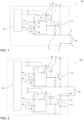
- FIG. 1 shows a schematic representation of a device 100 according to the disclosure.
- the device 100 in particular an electronic device, is provided for monitoring a switch-off capability of an electrical consumer 50 connected to a power supply 1, 3 via a first current path.
- the electrical consumer 50 is connected to the device 100 via the connections 2, 4.
- the connections 2, 4 represent an output that can be switched via a first control element 10.
- the first actuating element 10 is connected in the first current path and has an electrical connection to a voltage source.
- the first actuating element 10 can be designed as a field effect transistor.
- the current conduction capacity of the first actuating element 10 can be changed by means of a first actuating signal 11.
- the first actuating signal 11 can be a current or a voltage.
- the operating state of the first actuating element 10 can be characterized by a first electrical quantity, which is a first capacitance C GS10 at the first actuating element, and a first voltage U GS10 , which is determined by a voltage measuring device 30.
- the voltage measuring device 30 can determine/measure the first voltage at the gate-source path U GS10 of the first actuating element 10.
- the voltage measuring device 30 can be designed as an operational amplifier that receives the voltage at an input.
- the voltage measuring device 30 can be provided which determine and/or provide a value for the first voltage at the gate-source path U GS10 of the first actuating element 10.
- the first actuating element 10 is coupled to the voltage supply 1 by the drain connection. Furthermore, the first actuating element 10 is coupled to the load 50 by the source connection.
- the device 100 has a second actuating element 20 in a second current path.
- the second actuating element 20 can be designed as a field effect transistor.
- the second current path has a further power supply 5.
- the second actuating element 20 is designed to provide the first actuating signal 11 for controlling the first actuating element 10.
- the first actuating signal 11 is provided when the second actuating element 20 is in a switched state.
- the current conduction capacity of the second actuating element 20 can be changed by a second actuating signal 21.
- the second actuating signal 21 can be provided by a control device 60.
- the operating state of the second actuating element 20 can be characterized by a second electrical variable, which is a second capacitance C GS20 at the second actuating element 20 and causes a second voltage (gate-source voltage) U GS20 .
- first capacitance and the second capacitance are connected in series.
- a capacitive voltage divider is set up from the first and second capacitances.
- the drain-source capacitance of the second actuating element 20 and the gate-source capacitance thus form a capacitive voltage divider.
- control device 60 is provided in the device 100.
- the control device 60 can be designed as a microcontroller, FPGA, computer, PLC or the like.
- the control device 60 can be designed as a device that has an interface 62 that is set up to receive signals/data and to provide signals/data.
- the control device 60 is in particular designed to control the second actuating element 20 by means of the second actuating signal 21 at least in measuring intervals spaced apart from one another in time.
- the divided voltage can be queried and evaluated by the first voltage measuring device 30 to determine whether it is still in the range specified for confirming error-free shutdown. If the first actuating element 10 is broken, the voltage can be outside of a valid range. This can be used to diagnose that the first actuating element 10 can no longer be switched off. The values obtained for the first electrical quantity can thus be evaluated to detect a malfunction for switching off the first actuating element 10.
- Two capacitive paths are compared by measuring the voltage drop. If the capacitance of the gate-source path is smaller than the capacitance of the drain-source path, then the gate-source voltage is greater than the drain-source voltage and the first control element 10 should remain switched on.
- an analog-to-digital converter can be provided.
- the analog-digital converter can convert the detected first electrical quantity into a digital signal and provide it to the control device 60, shown in the Fig. 5 , via interface 62.
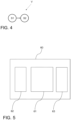
- the control device 60 has in particular a processor unit 61.
- the processor unit 61 is designed to provide control signals in order to control a second actuating element 20 at least in measuring intervals spaced apart from one another.
- the interface 62 is designed to provide control signals and to receive the obtained values of a first electrical variable of the first actuating element 10.
- the processor unit 61 is further designed to provide control signals in order to evaluate a detection of a malfunction for switching off the first actuating element 10, and wherein the evaluation includes a comparison of the obtained values of the first electrical variable with at least one reference default value.
- the processor unit 61 of the control device 60 can compare the digital signals of the analog-digital converter with the stored reference values and signal the detection of a malfunction for switching off the first actuating element 10.
- the control device 60 can provide a signal to this effect that is passed on to other devices for issuing a warning.
- control device 60 can control additional devices to trigger a warning.
- a further capacitance 13 is connected in series with the capacitance to be measured of the first actuating element 10 (junction capacitance). This allows the drain-source capacitance and thus the second actuating element 20 to be designed smaller.
- the additional capacitance 13 can be switched by the second actuating element 20.
- the capacitance 13 is selected such that in a capacitive voltage divider a corresponding voltage is still applied to the first actuating element 10 so that it switches.
- junction capacitance (gate-source) of the first actuating element 10 and the further capacitance 13 can be dimensioned such that they are in the same order of magnitude, for example in the range between 100 pF and 10 nF.
- the charge quantity of the junction capacitance of the first control element 10 is divided between the capacitive divider consisting of the further capacitance 13 (alternatively the capacitance of the drain-source path of the second control element 20).
- the divided voltage should be dimensioned such that the junction capacitance is sufficiently charged to continue to control the first control element 10.
- the divided voltage can be queried for a range within which it must lie.
- the voltage is outside the valid range. This means that it can be evaluated that the first actuating element 10 can no longer be switched off.
- the device 10 is designed in such a way that the output is switched off when no voltage is applied to the drain connection of the second actuating element 20.
- the switching energy is provided for the duration of a short test pulse.
- a resistor 51 can be provided which is dimensioned in such a way that any error from the second actuating element 20 cannot lead to the first actuating element 10 not switching off within a predetermined process safety time.
- the change in the drain-source voltage resulting from the capacitive discharge is measured. This can be done either via a circuit that only measures the alternating voltage component or via a bandpass filter if it is switched on and off cyclically at a certain frequency. The voltages could also be recorded and measured using an analog-digital converter. In this regard, the junction capacitance can be determined using a different/additional measuring principle.
- the junction capacitance can be determined via the discharge time.
- a test pulse can be started and the time that elapses until the voltage falls below a reference value can be measured.
- the device 100 according to the Fig. 3 a third actuating element 70.
- the third actuating element 70 is connected in the first current path in series with the first actuating element 10. If it is evaluated that the voltage has fallen below a predetermined reference value, the first actuating element 10 can no longer be switched off.
- the output 4, 2 and/or the electrical consumer 50 is/are switched off via a second switch-off path comprising the third actuating element 70.
- An error message is output and re-connection is prevented.
- the third actuating element 70 can be controlled via the control device 60.
- FIG. 2 A further embodiment of the device is explained.
- the above-mentioned reference to Fig. 1 The first embodiment of the device explained above is based on the above-mentioned principle; identical or equivalent elements are provided with the same reference symbols and will not be described again in detail.
- the Fig. 2 the disclosed system 200.
- the system 200 comprises a first and a second device 100 according to the disclosure.
- the first and the second device 100 are duplicated and are arranged such that the negative pole of the first (upper) device (100) is coupled to the positive pole of the (lower) device 100.
- the system 200 also comprises an output 201 for tapping the voltage at the negative pole.
- the first device 100 and the second device couple a consumer 50.
- a second shutdown channel is provided.
- the two devices 100 for switching the plus and minus channels mean that a second shutdown channel remains even in the event of a cross-circuit outside the device. If the consumer 50 is supplied with power from an external source on the plus channel due to a fault, the second device 100 (as an M switch) can still prevent the flow of current. If the case occurs in which there is a ground fault on the minus channel of the consumer 50, the first device 100 (as a P switch) can still prevent the flow of current.
- Fig. 4 shows a flow chart of a method according to the disclosure.
- the reference symbol V designates an embodiment of the method according to the disclosure.
- the method V for monitoring a switch-off capability has several method steps.
- the method V can be carried out by the processor unit 61 of the control device 60.
- the second actuating element 20 is controlled by means of the second actuating signal 21 at least in measuring intervals spaced apart from one another in time.
- values of the first electrical variable obtained in this process are evaluated for detection of a malfunction for switching off the first actuating element 10.
Landscapes
- Physics & Mathematics (AREA)
- General Physics & Mathematics (AREA)
- Engineering & Computer Science (AREA)
- Microelectronics & Electronic Packaging (AREA)
- Electronic Switches (AREA)
- Emergency Protection Circuit Devices (AREA)
Applications Claiming Priority (1)
| Application Number | Priority Date | Filing Date | Title |
|---|---|---|---|
| DE102023116488.0A DE102023116488A1 (de) | 2023-06-22 | 2023-06-22 | Vorrichtung und Verfahren zum Überwachen einer Abschaltfähigkeit |
Publications (1)
| Publication Number | Publication Date |
|---|---|
| EP4481411A1 true EP4481411A1 (fr) | 2024-12-25 |
Family
ID=91617237
Family Applications (1)
| Application Number | Title | Priority Date | Filing Date |
|---|---|---|---|
| EP24183030.6A Pending EP4481411A1 (fr) | 2023-06-22 | 2024-06-19 | Dispositif et procédé de surveillance d'une capacité de coupure |
Country Status (4)
| Country | Link |
|---|---|
| US (1) | US12153081B1 (fr) |
| EP (1) | EP4481411A1 (fr) |
| CN (1) | CN119178937B (fr) |
| DE (1) | DE102023116488A1 (fr) |
Citations (6)
| Publication number | Priority date | Publication date | Assignee | Title |
|---|---|---|---|---|
| EP1335471A2 (fr) | 2002-02-08 | 2003-08-13 | Tyco Electronics Corporation | Relais à semi-conducteurs |
| US7702302B1 (en) | 2005-12-12 | 2010-04-20 | Linear Technology Corporation | Combination of high-side and low-side current control in system for providing power over communication link |
| US20120161817A1 (en) | 2010-12-27 | 2012-06-28 | Denso Corporation | Electrical load driving apparatus |
| US20190056448A1 (en) * | 2017-08-16 | 2019-02-21 | Infineon Technologies Ag | Testing mos power switches |
| DE102020113822A1 (de) | 2019-06-13 | 2020-12-17 | Turck Holding Gmbh | Vorrichtung und Verfahren zur elektrischen Stromkreisüberwachung |
| DE102022118881A1 (de) * | 2021-09-20 | 2023-03-23 | Infineon Technologies Ag | Treiberschaltung, verfahren und system für gate-zu-source-überwachung von leistungsschaltern während der laufzeit |
Family Cites Families (10)
| Publication number | Priority date | Publication date | Assignee | Title |
|---|---|---|---|---|
| US4893158A (en) | 1987-06-22 | 1990-01-09 | Nissan Motor Co., Ltd. | MOSFET device |
| US8299820B2 (en) * | 2008-09-30 | 2012-10-30 | Infineon Technologies Austria Ag | Circuit including a resistor arrangement for actuation of a transistor |
| EP2180392A1 (fr) * | 2008-10-22 | 2010-04-28 | Micronas GmbH | Alimentation en courant électrique |
| EP2980660B1 (fr) * | 2014-07-28 | 2016-11-23 | Pepperl & Fuchs GmbH | Procédé et dispositif de surveillance et de commutation d'un circuit de charge |
| DE102015121194A1 (de) | 2015-12-04 | 2017-06-08 | Infineon Technologies Ag | Vorrichtung mit integriertem Schutzverlauf und Verfahren |
| US10707856B2 (en) | 2017-09-19 | 2020-07-07 | Infineon Technologies Ag | MOS power transistors in parallel channel configuration |
| US10451669B2 (en) * | 2017-09-29 | 2019-10-22 | Infineon Technologies Ag | Evaluating a gate-source leakage current in a transistor device |
| US10895601B2 (en) * | 2019-05-10 | 2021-01-19 | Infineon Technologies Ag | System and method of monitoring a switching transistor |
| EP3748794A1 (fr) * | 2019-06-05 | 2020-12-09 | Siemens Aktiengesellschaft | Protection électronique pour une alimentation électrique |
| DE102021206219A1 (de) | 2021-06-17 | 2022-12-22 | Robert Bosch Gesellschaft mit beschränkter Haftung | Schaltungsanordnung zum Messen einer elektrischen Spannung |
-
2023
- 2023-06-22 DE DE102023116488.0A patent/DE102023116488A1/de active Pending
-
2024
- 2024-06-18 CN CN202410781906.5A patent/CN119178937B/zh active Active
- 2024-06-19 EP EP24183030.6A patent/EP4481411A1/fr active Pending
- 2024-06-20 US US18/748,409 patent/US12153081B1/en active Active
Patent Citations (6)
| Publication number | Priority date | Publication date | Assignee | Title |
|---|---|---|---|---|
| EP1335471A2 (fr) | 2002-02-08 | 2003-08-13 | Tyco Electronics Corporation | Relais à semi-conducteurs |
| US7702302B1 (en) | 2005-12-12 | 2010-04-20 | Linear Technology Corporation | Combination of high-side and low-side current control in system for providing power over communication link |
| US20120161817A1 (en) | 2010-12-27 | 2012-06-28 | Denso Corporation | Electrical load driving apparatus |
| US20190056448A1 (en) * | 2017-08-16 | 2019-02-21 | Infineon Technologies Ag | Testing mos power switches |
| DE102020113822A1 (de) | 2019-06-13 | 2020-12-17 | Turck Holding Gmbh | Vorrichtung und Verfahren zur elektrischen Stromkreisüberwachung |
| DE102022118881A1 (de) * | 2021-09-20 | 2023-03-23 | Infineon Technologies Ag | Treiberschaltung, verfahren und system für gate-zu-source-überwachung von leistungsschaltern während der laufzeit |
Also Published As
| Publication number | Publication date |
|---|---|
| CN119178937A (zh) | 2024-12-24 |
| US12153081B1 (en) | 2024-11-26 |
| DE102023116488A1 (de) | 2024-12-24 |
| CN119178937B (zh) | 2026-04-24 |
Similar Documents
| Publication | Publication Date | Title |
|---|---|---|
| DE102010007784A1 (de) | Vorrichtung zur elektrischen Stromkreisüberwachung | |
| EP1980019A1 (fr) | Ensemble circuit pourvu d'une protection contre l'alimentation en retour et servant a effectuer une commutation dans des applications de puissance | |
| DE102016109137B3 (de) | Überwachungsvorrichtung und Überwachungsverfahren | |
| DE10118189A1 (de) | Verfahren und Vorrichtung zum Abfragen eines Schaltzustandes eines Schalters | |
| DE102011107734B4 (de) | Schaltungsanordnung zum Schalten eines Relais in einen sicheren Schaltzustand | |
| EP4012926B1 (fr) | Commutateur à courant continu | |
| EP2342946A1 (fr) | Circuit et procédé pour faire fonctionner une oled | |
| EP1594021B1 (fr) | Dispositif de circuit et procédé de test de contacts de commutation d'un circuit numérique de sortie | |
| DE102008029680B4 (de) | Verfahren und elektronische Schaltung für eine elektronische Schaltungseinheit | |
| WO2023011768A1 (fr) | Unité de disjoncteur | |
| EP4481411A1 (fr) | Dispositif et procédé de surveillance d'une capacité de coupure | |
| DE102012111070B4 (de) | Sicherheitsbezogene Vorrichtung zum sicheren Schalten einer elektrischen Last | |
| DE19604041C1 (de) | Schaltungsanordnung zur Erkennung eines durch eine Last fließenden Laststroms | |
| EP2503669B1 (fr) | Système d'automatisation de sécurite avec comportement de commutation contrôlé et avec dispositif d'accélération de commutation | |
| EP3314765B1 (fr) | Montage de circuits pour sortie de circuit numérique sûre et module de sortie ainsi que procédé de contrôle d'un tel montage de circuits | |
| EP2874258A2 (fr) | Circuit électronique | |
| EP3709513B1 (fr) | Dispositif de commutation ainsi que procédé de fonctionnement d'un dispositif de commutation | |
| EP2876509B1 (fr) | Commande de sécurité | |
| WO2009103584A1 (fr) | Procédé et dispositif pour faire fonctionner une unité de commutation | |
| DE102020210339B4 (de) | Schaltungsanordnung und Verfahren zur Fehlererkennung | |
| DE102008029679B4 (de) | System, Verfahren und elektronische Schaltung für mindestens eine elektronische Schaltungseinheit | |
| DE202014004493U1 (de) | Elektronisches Relais | |
| DE102019204429A1 (de) | Schutzvorrichtung für eine Treiberschaltung und Verfahren zum Schutz einer Treiberschaltung | |
| DE102011015220B4 (de) | Kommunikationssystem mit überwachtem Eingangszustand einer Eingangseinrichtung sowie Stromerhöhungseinrichtung | |
| DE102008008047A1 (de) | Externer Watchdog sowie Schaltgerät, insbesondere Niederspannungsschaltgerät, mit einem externen Watchdog |
Legal Events
| Date | Code | Title | Description |
|---|---|---|---|
| PUAI | Public reference made under article 153(3) epc to a published international application that has entered the european phase |
Free format text: ORIGINAL CODE: 0009012 |
|
| STAA | Information on the status of an ep patent application or granted ep patent |
Free format text: STATUS: THE APPLICATION HAS BEEN PUBLISHED |
|
| AK | Designated contracting states |
Kind code of ref document: A1 Designated state(s): AL AT BE BG CH CY CZ DE DK EE ES FI FR GB GR HR HU IE IS IT LI LT LU LV MC ME MK MT NL NO PL PT RO RS SE SI SK SM TR |
|
| STAA | Information on the status of an ep patent application or granted ep patent |
Free format text: STATUS: REQUEST FOR EXAMINATION WAS MADE |
|
| STAA | Information on the status of an ep patent application or granted ep patent |
Free format text: STATUS: EXAMINATION IS IN PROGRESS |
|
| 17P | Request for examination filed |
Effective date: 20250521 |
|
| 17Q | First examination report despatched |
Effective date: 20250618 |