EP4482279A1 - Dispositif électronique comprenant une caméra udc - Google Patents
Dispositif électronique comprenant une caméra udc Download PDFInfo
- Publication number
- EP4482279A1 EP4482279A1 EP23792061.6A EP23792061A EP4482279A1 EP 4482279 A1 EP4482279 A1 EP 4482279A1 EP 23792061 A EP23792061 A EP 23792061A EP 4482279 A1 EP4482279 A1 EP 4482279A1
- Authority
- EP
- European Patent Office
- Prior art keywords
- area
- pixel
- subpixel
- display
- electronic device
- Prior art date
- Legal status (The legal status is an assumption and is not a legal conclusion. Google has not performed a legal analysis and makes no representation as to the accuracy of the status listed.)
- Granted
Links
Images












Classifications
-
- G—PHYSICS
- G09—EDUCATION; CRYPTOGRAPHY; DISPLAY; ADVERTISING; SEALS
- G09G—ARRANGEMENTS OR CIRCUITS FOR CONTROL OF INDICATING DEVICES USING STATIC MEANS TO PRESENT VARIABLE INFORMATION
- G09G3/00—Control arrangements or circuits, of interest only in connection with visual indicators other than cathode-ray tubes
- G09G3/20—Control arrangements or circuits, of interest only in connection with visual indicators other than cathode-ray tubes for presentation of an assembly of a number of characters, e.g. a page, by composing the assembly by combination of individual elements arranged in a matrix no fixed position being assigned to or needed to be assigned to the individual characters or partial characters
- G09G3/22—Control arrangements or circuits, of interest only in connection with visual indicators other than cathode-ray tubes for presentation of an assembly of a number of characters, e.g. a page, by composing the assembly by combination of individual elements arranged in a matrix no fixed position being assigned to or needed to be assigned to the individual characters or partial characters using controlled light sources
- G09G3/30—Control arrangements or circuits, of interest only in connection with visual indicators other than cathode-ray tubes for presentation of an assembly of a number of characters, e.g. a page, by composing the assembly by combination of individual elements arranged in a matrix no fixed position being assigned to or needed to be assigned to the individual characters or partial characters using controlled light sources using electroluminescent panels
- G09G3/32—Control arrangements or circuits, of interest only in connection with visual indicators other than cathode-ray tubes for presentation of an assembly of a number of characters, e.g. a page, by composing the assembly by combination of individual elements arranged in a matrix no fixed position being assigned to or needed to be assigned to the individual characters or partial characters using controlled light sources using electroluminescent panels semiconductive, e.g. using light-emitting diodes [LED]
- G09G3/3208—Control arrangements or circuits, of interest only in connection with visual indicators other than cathode-ray tubes for presentation of an assembly of a number of characters, e.g. a page, by composing the assembly by combination of individual elements arranged in a matrix no fixed position being assigned to or needed to be assigned to the individual characters or partial characters using controlled light sources using electroluminescent panels semiconductive, e.g. using light-emitting diodes [LED] organic, e.g. using organic light-emitting diodes [OLED]
-
- H—ELECTRICITY
- H10—SEMICONDUCTOR DEVICES; ELECTRIC SOLID-STATE DEVICES NOT OTHERWISE PROVIDED FOR
- H10D—INORGANIC ELECTRIC SEMICONDUCTOR DEVICES
- H10D86/00—Integrated devices formed in or on insulating or conducting substrates, e.g. formed in silicon-on-insulator [SOI] substrates or on stainless steel or glass substrates
- H10D86/40—Integrated devices formed in or on insulating or conducting substrates, e.g. formed in silicon-on-insulator [SOI] substrates or on stainless steel or glass substrates characterised by multiple TFTs
- H10D86/421—Integrated devices formed in or on insulating or conducting substrates, e.g. formed in silicon-on-insulator [SOI] substrates or on stainless steel or glass substrates characterised by multiple TFTs having a particular composition, shape or crystalline structure of the active layer
-
- H—ELECTRICITY
- H10—SEMICONDUCTOR DEVICES; ELECTRIC SOLID-STATE DEVICES NOT OTHERWISE PROVIDED FOR
- H10K—ORGANIC ELECTRIC SOLID-STATE DEVICES
- H10K50/00—Organic light-emitting devices
-
- H—ELECTRICITY
- H10—SEMICONDUCTOR DEVICES; ELECTRIC SOLID-STATE DEVICES NOT OTHERWISE PROVIDED FOR
- H10K—ORGANIC ELECTRIC SOLID-STATE DEVICES
- H10K50/00—Organic light-emitting devices
- H10K50/10—OLEDs or polymer light-emitting diodes [PLED]
- H10K50/11—OLEDs or polymer light-emitting diodes [PLED] characterised by the electroluminescent [EL] layers
-
- H—ELECTRICITY
- H10—SEMICONDUCTOR DEVICES; ELECTRIC SOLID-STATE DEVICES NOT OTHERWISE PROVIDED FOR
- H10K—ORGANIC ELECTRIC SOLID-STATE DEVICES
- H10K50/00—Organic light-emitting devices
- H10K50/80—Constructional details
-
- H—ELECTRICITY
- H10—SEMICONDUCTOR DEVICES; ELECTRIC SOLID-STATE DEVICES NOT OTHERWISE PROVIDED FOR
- H10K—ORGANIC ELECTRIC SOLID-STATE DEVICES
- H10K50/00—Organic light-emitting devices
- H10K50/80—Constructional details
- H10K50/805—Electrodes
- H10K50/81—Anodes
- H10K50/813—Anodes characterised by their shape
-
- H—ELECTRICITY
- H10—SEMICONDUCTOR DEVICES; ELECTRIC SOLID-STATE DEVICES NOT OTHERWISE PROVIDED FOR
- H10K—ORGANIC ELECTRIC SOLID-STATE DEVICES
- H10K50/00—Organic light-emitting devices
- H10K50/80—Constructional details
- H10K50/805—Electrodes
- H10K50/81—Anodes
- H10K50/816—Multilayers, e.g. transparent multilayers
-
- H—ELECTRICITY
- H10—SEMICONDUCTOR DEVICES; ELECTRIC SOLID-STATE DEVICES NOT OTHERWISE PROVIDED FOR
- H10K—ORGANIC ELECTRIC SOLID-STATE DEVICES
- H10K50/00—Organic light-emitting devices
- H10K50/80—Constructional details
- H10K50/85—Arrangements for extracting light from the devices
- H10K50/858—Arrangements for extracting light from the devices comprising refractive means, e.g. lenses
-
- H—ELECTRICITY
- H10—SEMICONDUCTOR DEVICES; ELECTRIC SOLID-STATE DEVICES NOT OTHERWISE PROVIDED FOR
- H10K—ORGANIC ELECTRIC SOLID-STATE DEVICES
- H10K59/00—Integrated devices, or assemblies of multiple devices, comprising at least one organic light-emitting element covered by group H10K50/00
-
- H—ELECTRICITY
- H10—SEMICONDUCTOR DEVICES; ELECTRIC SOLID-STATE DEVICES NOT OTHERWISE PROVIDED FOR
- H10K—ORGANIC ELECTRIC SOLID-STATE DEVICES
- H10K59/00—Integrated devices, or assemblies of multiple devices, comprising at least one organic light-emitting element covered by group H10K50/00
- H10K59/10—OLED displays
- H10K59/12—Active-matrix OLED [AMOLED] displays
- H10K59/121—Active-matrix OLED [AMOLED] displays characterised by the geometry or disposition of pixel elements
-
- H—ELECTRICITY
- H10—SEMICONDUCTOR DEVICES; ELECTRIC SOLID-STATE DEVICES NOT OTHERWISE PROVIDED FOR
- H10K—ORGANIC ELECTRIC SOLID-STATE DEVICES
- H10K59/00—Integrated devices, or assemblies of multiple devices, comprising at least one organic light-emitting element covered by group H10K50/00
- H10K59/10—OLED displays
- H10K59/12—Active-matrix OLED [AMOLED] displays
- H10K59/121—Active-matrix OLED [AMOLED] displays characterised by the geometry or disposition of pixel elements
- H10K59/1213—Active-matrix OLED [AMOLED] displays characterised by the geometry or disposition of pixel elements the pixel elements being TFTs
-
- H—ELECTRICITY
- H10—SEMICONDUCTOR DEVICES; ELECTRIC SOLID-STATE DEVICES NOT OTHERWISE PROVIDED FOR
- H10K—ORGANIC ELECTRIC SOLID-STATE DEVICES
- H10K59/00—Integrated devices, or assemblies of multiple devices, comprising at least one organic light-emitting element covered by group H10K50/00
- H10K59/10—OLED displays
- H10K59/12—Active-matrix OLED [AMOLED] displays
- H10K59/124—Insulating layers formed between TFT elements and OLED elements
-
- H—ELECTRICITY
- H10—SEMICONDUCTOR DEVICES; ELECTRIC SOLID-STATE DEVICES NOT OTHERWISE PROVIDED FOR
- H10K—ORGANIC ELECTRIC SOLID-STATE DEVICES
- H10K59/00—Integrated devices, or assemblies of multiple devices, comprising at least one organic light-emitting element covered by group H10K50/00
- H10K59/10—OLED displays
- H10K59/12—Active-matrix OLED [AMOLED] displays
- H10K59/131—Interconnections, e.g. wiring lines or terminals
-
- H—ELECTRICITY
- H10—SEMICONDUCTOR DEVICES; ELECTRIC SOLID-STATE DEVICES NOT OTHERWISE PROVIDED FOR
- H10K—ORGANIC ELECTRIC SOLID-STATE DEVICES
- H10K59/00—Integrated devices, or assemblies of multiple devices, comprising at least one organic light-emitting element covered by group H10K50/00
- H10K59/30—Devices specially adapted for multicolour light emission
- H10K59/35—Devices specially adapted for multicolour light emission comprising red-green-blue [RGB] subpixels
-
- H—ELECTRICITY
- H10—SEMICONDUCTOR DEVICES; ELECTRIC SOLID-STATE DEVICES NOT OTHERWISE PROVIDED FOR
- H10K—ORGANIC ELECTRIC SOLID-STATE DEVICES
- H10K59/00—Integrated devices, or assemblies of multiple devices, comprising at least one organic light-emitting element covered by group H10K50/00
- H10K59/30—Devices specially adapted for multicolour light emission
- H10K59/35—Devices specially adapted for multicolour light emission comprising red-green-blue [RGB] subpixels
- H10K59/353—Devices specially adapted for multicolour light emission comprising red-green-blue [RGB] subpixels characterised by the geometrical arrangement of the RGB subpixels
-
- H—ELECTRICITY
- H10—SEMICONDUCTOR DEVICES; ELECTRIC SOLID-STATE DEVICES NOT OTHERWISE PROVIDED FOR
- H10K—ORGANIC ELECTRIC SOLID-STATE DEVICES
- H10K59/00—Integrated devices, or assemblies of multiple devices, comprising at least one organic light-emitting element covered by group H10K50/00
- H10K59/60—OLEDs integrated with inorganic light-sensitive elements, e.g. with inorganic solar cells or inorganic photodiodes
- H10K59/65—OLEDs integrated with inorganic image sensors
-
- G—PHYSICS
- G09—EDUCATION; CRYPTOGRAPHY; DISPLAY; ADVERTISING; SEALS
- G09G—ARRANGEMENTS OR CIRCUITS FOR CONTROL OF INDICATING DEVICES USING STATIC MEANS TO PRESENT VARIABLE INFORMATION
- G09G2300/00—Aspects of the constitution of display devices
- G09G2300/04—Structural and physical details of display devices
- G09G2300/0421—Structural details of the set of electrodes
- G09G2300/0426—Layout of electrodes and connections
-
- G—PHYSICS
- G09—EDUCATION; CRYPTOGRAPHY; DISPLAY; ADVERTISING; SEALS
- G09G—ARRANGEMENTS OR CIRCUITS FOR CONTROL OF INDICATING DEVICES USING STATIC MEANS TO PRESENT VARIABLE INFORMATION
- G09G2320/00—Control of display operating conditions
- G09G2320/02—Improving the quality of display appearance
- G09G2320/0233—Improving the luminance or brightness uniformity across the screen
-
- G—PHYSICS
- G09—EDUCATION; CRYPTOGRAPHY; DISPLAY; ADVERTISING; SEALS
- G09G—ARRANGEMENTS OR CIRCUITS FOR CONTROL OF INDICATING DEVICES USING STATIC MEANS TO PRESENT VARIABLE INFORMATION
- G09G2320/00—Control of display operating conditions
- G09G2320/04—Maintaining the quality of display appearance
- G09G2320/043—Preventing or counteracting the effects of ageing
Definitions
- the disclosure relates to an electronic device including an under display camera (UDC).
- UDC under display camera
- An electronic device may include at least one camera.
- the electronic device may include at least one camera disposed around a display or overlapping with at least a portion of the display.
- UDC under display camera
- an electronic device in which the UDC is disposed under the active area of the display needs to increase transmittance in at least a portion (hereinafter referred to as "UDC area") of the display overlapping with the UDC in order to increase the amount of light introduced into the UDC.
- UDC area a portion of the display overlapping with the UDC in order to increase the amount of light introduced into the UDC.
- a method of forming, in the UDC area, a transmission area in which no pixels and/or lines are formed by lowering the arrangement density of pixels and/or lines of the display may be proposed.
- a plurality of first pixels in the UDC area may be disposed to have a first density
- a plurality of second pixels in a normal area e.g., an area not overlapping with the UDC
- a normal area e.g., an area not overlapping with the UDC
- An electronic device including a UDC may require a technique for reducing a visibility problem that a UDC area is recognized by a user due to a decrease in the arrangement density of a plurality of first pixels disposed in the UDC area.
- an electronic device including a UDC may require a technique for reducing the luminance difference.
- An electronic device including a UDC may require a design for reducing not only a luminance difference between a UDC area and a normal area, but also a difference between the lifespans of second pixels disposed in the normal area and the lifespans of first pixels disposed in the UDC area.
- Embodiments of the disclosure may provide an electronic device capable of increasing the transmittance of a UDC area and reducing a luminance difference and/or lifetime difference between first pixels disposed in the UDC area and second pixels disposed in a normal area, by changing the structure of the first pixel disposed in the UDC area and/or the shape of a driving circuit for driving the first pixel.
- Embodiments of the disclosure may provide an electronic device capable of reducing a visibility problem in which a UDC area is viewed by a user, by changing the structure of a first pixel disposed in the UDC area.
- An electronic device includes: a housing; a display; and a camera disposed inside the housing overlapping a portion of the display and configured to acquire light passing through the display from outside, wherein the display includes a first area in which a first pixel overlapping with at least a portion of the camera and a first pixel driving circuit for driving the first pixel are disposed, and a second area, other than the first area, in which a second pixel and a second pixel driving circuit for driving the second pixel are disposed, wherein the first pixel driving circuit includes: a first driving thin film transistor (TFT) having a first channel region having a straight shape that does not include a curved shape, wherein the second pixel driving circuit includes: a second driving TFT having a second channel region having a curved shape, wherein a first channel width of the first driving TFT is greater than a second channel width of the second driving TFT, and wherein a first channel length of the first driving TFT is less than a second channel length of the second driving
- TFT thin
- An electronic device can increase the transmittance of a UDC area and reduce a luminance difference and/or lifetime difference between first pixels disposed in the UDC area and second pixels disposed in a normal area, by changing the structure of the first pixel disposed in the UDC area and/or the shape of a driving circuit for driving the first pixel.
- An electronic device can reduce a visibility problem in which a UDC area is viewed by a user, by changing the structure of a first pixel disposed in the UDC area.
- FIG. 1 is a front perspective view of an electronic device 100 according to various embodiments.
- FIG. 2 is a rear perspective view of the electronic device 100 of FIG. 1 according to various embodiments.
- the electronic device 100 may include a housing 110 having a first surface (or a front surface) 110A, a second surface (or a rear surface) 110B, and a side surface 110C surrounding a space between the first surface 110A and the second surface 110B.
- the housing 110 may refer to a structure that forms some of the first surface 110A, the second surface 110B, and the side surface 110C.
- the first surface 110A may be formed by a front plate 102 (e.g., a glass plate including various coating layers, or a polymer plate) that is substantially transparent at least in part.
- the second surface 110B may be formed by a substantially opaque rear plate 111.
- the rear plate 111 may be formed, for example, of coated or colored glass, ceramic, polymer, metal (e.g., aluminum, stainless steel (STS), or magnesium), or a combination of at least two of the foregoing materials.
- the side surface 110C may be combined with the front plate 102 and the rear plate 111 and formed by a lateral bezel structure 118 (or "lateral member") including metal and/or polymer.
- the rear surface plate 111 and the lateral bezel structure 118 may be integrally formed and include the same material (e.g., a metal material such as aluminum).
- the electronic device 100 may include at least one of a display 101, an input device 103, sound output devices 107 and 114, sensor modules 104 and 119, cameras 105 and 112, a key input device 117, an indicator (not shown), and connectors 108 and 109.
- the electronic device 100 may omit at least one (e.g., the key input device 117, the connectors 108 and 109, or the indicator) of the above components or additionally include other components.
- the display 101 may be visible through a portion of the front plate 102, for example. In various embodiments, at least a portion of the display 101 may be viewed through the front plate 102 forming the first surface 110A. In various embodiments, the edge of the display 101 may be substantially identical to an adjacent outer shape of the front plate 102. In an embodiment (not shown), in order to expand the area where the display 101 is visible (as used herein with reference to the display, the terms "exposed”, “visible”, “visually exposed”, etc. may be used interchangeably and include a display having a cover layer, cover sheet, cover plate, or the like), a distance between the periphery of the display 101 and the periphery of the front plate 102 may be substantially unchanged.
- the surface (or the front plate 102) of the housing 110 may include a screen display area formed as the display 101 is visually exposed (e.g., visible).
- the screen display area may include a camera overlapping area A1 (e.g., a first area) in which the first camera 105 is disposed below (e.g., in the z2 direction), and a normal display area A2 (e.g., a second area) where no camera is disposed below (e.g., in the z2 direction).
- the screen display area may further include a sensor overlapping area (not shown) in which at least one sensor module (not shown) is disposed below (e.g., in the z2 direction).
- the at least one sensor module may be a sensor of various types that operates by acquiring external light.
- the cameras 105 and 112 may include the first camera 105 disposed on the first surface 110A of the electronic device 100 and/or the second camera 112 disposed on the second surface 110B.
- the cameras 105 and 112 may include one or more lenses, an image sensor, and/or an image signal processor.
- the cameras 105 and 112 may further include a flash 113.
- two or more lenses (wide-angle lens, ultra-wide-angle lens, or telephoto lens) and image sensors may be disposed on the first surface 110A or the second surface 110B of the electronic device 100.
- the electronic device 100 may include a plurality of cameras 105 and 112.
- the electronic device 100 may include a plurality of cameras (e.g., a dual camera or a triple camera) having different properties (e.g., angle of view) or functions.
- a plurality of cameras 105 and 112 including lenses with different angles of view, and the electronic device 100 may control the angles of view of the cameras 105 and 112 to be changed in response to a user's selection.
- the plurality of cameras 105 and 112 may include at least one of a wide-angle camera, a telephoto camera, a color camera, a monochrome camera, or an infrared (IR) camera (e.g., a time of flight (TOF) camera, a structured light camera).
- the IR camera may operate as at least a part of the sensor module.
- the first camera 105 may be disposed under (e.g., in the z2 direction) the camera overlapping area A1 of the display.
- the first camera 105 may be referred to as an under display camera (UDC).
- UDC under display camera
- the first camera 105 is disposed under (e.g., in the z2 direction) the camera overlapping area A1 of the display, the position of the first camera 105 may not be visually distinguished (or exposed).
- the first camera 105 when the display 101 is viewed from above (e.g., the z1 direction), the first camera 105 is disposed in the camera overlapping area A1, which is a part of the display, not to be visually exposed to the outside, and it can acquire an image of an external subject.
- the first camera 105 may be disposed to overlap with at least a part of the camera overlapping area A1 and not to be visually exposed, thus acquiring an image of an external subject.
- a recess or an opening may be formed in a portion of a screen display area (e.g., the first surface 110A or the first area 110D) of the display 101, and at least one of the sound output device 114, the sensor module 104, a light emitting device (e.g., the flash), and the camera 105 may be included to be aligned at least in part with the recess or the opening.
- at least one of the sound output device 114, the sensor module 119, the light emitting device (e.g., the flash), and the camera 112 may be included under the screen display area of the display 101.
- the display 101 may be disposed to be combined with or adjacent to a touch sensing circuit, a pressure sensor capable of measuring the intensity (pressure) of a touch, and/or a digitizer for detecting a magnetic stylus pen.
- the input device 103 may include a microphone 103.
- the input device 103 may include a plurality of microphones 103 disposed to detect the direction of sound.
- the sound output devices 107 and 114 may include speakers 107 and 114.
- the speakers 107 and 114 may include an external speaker 107 and a call receiver 114.
- the microphone 103, the speakers 107 and 114, and the connectors 108 and 109 may be disposed in the space of the electronic device 100 and exposed to the external environment through at least one hole formed in the housing 110.
- the hole formed in the housing 110 may be commonly used for the microphone 103 and the speakers 107 and 114.
- the sound output devices 107 and 114 may include a speaker (e.g., a piezo speaker) that operates without any hole formed in the housing 110.
- the sensor modules 104 and 119 may generate electrical signals or data values corresponding to an internal operating state of the electronic device 100 or an external environmental state.
- the sensor modules 104 and 119 may include, for example, a first sensor module 104 (e.g., a proximity sensor) and/or a second sensor module (not shown) (e.g., a fingerprint sensor) disposed on the first surface 110A of the housing 110, and/or a third sensor module 119 (e.g., an HRM sensor) disposed on the second surface 110B of the housing 110.
- the fingerprint sensor may be disposed under the first surface 110A of the housing 110, a portion of the second surface 110B, or the display 101.
- the electronic device 100 may further include a sensor module (not shown), for example, at least one of a gesture sensor, a gyro sensor, an air pressure sensor, a magnetic sensor, an acceleration sensor, a grip sensor, a color sensor, an infrared (IR) sensor, a bio sensor, a temperature sensor, a humidity sensor, or an illuminance sensor.
- a sensor module for example, at least one of a gesture sensor, a gyro sensor, an air pressure sensor, a magnetic sensor, an acceleration sensor, a grip sensor, a color sensor, an infrared (IR) sensor, a bio sensor, a temperature sensor, a humidity sensor, or an illuminance sensor.
- the electronic device 100 may have a bar-type or plate-type appearance, but the disclosure is not limited thereto.
- the electronic device 100 may include various forms of electronic devices such as a foldable electronic device, a slidable electronic device, a stretchable electronic device, and/or a rollable electronic device.
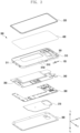
- FIG. 3 is an exploded perspective view of the electronic device 100 of FIG. 1 according to various embodiments.
- the electronic device 300 of FIG. 3 may be similar at least in part to the electronic device 100 of FIGS. 1 and 2 or further include various embodiments of the electronic device.
- an electronic device 300 may include a lateral member 310 (e.g., the lateral bezel structure 118 in FIG. 1 ), a first support member 311 (e.g., a bracket or support structure), a front plate 320 (e.g., a front cover, the front plate 102 in FIG. 1 ), a display 400 (e.g., the display 101 in FIG.
- a lateral member 310 e.g., the lateral bezel structure 118 in FIG. 1
- a first support member 311 e.g., a bracket or support structure
- a front plate 320 e.g., a front cover, the front plate 102 in FIG. 1
- a display 400 e.g., the display 101 in FIG.
- the electronic device 300 may omit at least one (e.g., the first support member 311 or the second support member 360) of the above components or additionally include other components. At least one of the components of the electronic device 300 may be identical to or similar to at least one of the components of the electronic device 100 in FIG. 1 or 2 , and thus overlapping descriptions may not be repeated hereinafter.
- the first support member 311 may be disposed inside the electronic device 300 and connected to the lateral member 310 or integrally formed with the lateral member 310.
- the first support member 311 may be formed of, for example, a metal material and/or a non-metal (e.g., polymer) material.
- the first support member 311 may be combined with the display 400 on one surface thereof and combined with the printed circuit board 340 on the other surface.
- a processor, a memory, and/or an interface may be mounted on the printed circuit board 340.
- the processor may include, for example, one or more of a central processing unit, an application processor, a graphics processing unit, an image signal processor, a sensor hub processor, or a communication processor.
- the memory may include, for example, a volatile memory or a non-volatile memory.
- the interface may include, for example, a high definition multimedia interface (HDMI), a universal serial bus (USB) interface, an SD card interface, and/or an audio interface.
- HDMI high definition multimedia interface
- USB universal serial bus
- the interface may electrically or physically connect the electronic device 300 to an external electronic device, and may include a USB connector, an SD card/MMC connector, or an audio connector.
- the battery 350 is a device for supplying power to at least one component of the electronic device 300 and may include, for example, a non-rechargeable primary battery, a rechargeable secondary battery, or a fuel cell. At least a portion of the battery 350 may be disposed, for example, substantially on the same plane as the printed circuit board 340.
- the battery 350 may be integrally disposed inside the electronic device 300. In an embodiment, the battery 350 may be detachably disposed in the electronic device 300.
- the antenna 370 may be disposed between the rear plate 380 and the battery 350.
- the antenna 370 may include, for example, a near field communication (NFC) antenna, a wireless charging antenna, and/or a magnetic secure transmission (MST) antenna.
- the antenna 370 may, for example, perform short-range communication with an external device or wirelessly transmit/receive power required for charging.
- an antenna structure may be formed by a part of the lateral bezel structure 310 and/or a part of the first support member 311 or a combination thereof.
- the second support member 360 (e.g., a rear case) may be disposed between the printed circuit board 340 and the antenna 370.
- the second support member 360 may have one surface where at least one of the printed circuit board 340 or the battery 350 is combined, and the other surface where the antenna 370 is combined.
- the first support member 311 of the lateral member 310 may have a first surface 3101 facing the front surface plate 320 and a second surface 3102 facing a direction (e.g., the direction of the rear surface plate 380) opposite to the first surface 3101.
- the camera 105 e.g., the first camera 105 in FIG. 1
- the camera 105 may be disposed between the first support member 311 and the rear plate 380.
- the camera 105 may be disposed to be protruded or visible in the direction of the front surface plate 320 through a through-hole 301 connected from the first surface 3101 to the second surface 3102 of the first support member 311.
- a portion protruding through the through-hole 301 of the camera 105 may be disposed to detect an external environment at a corresponding position of the display 400.
- the through-hole 301 may be unnecessary.
- FIG. 4 is an exploded perspective view of the display 400 shown in FIG. 3 according to various embodiments.
- the display 400 of FIG. 4 may be similar at least in part to the display 101 of FIG. 1 and the display 400 of FIG. 3 or further include various embodiments of the display.
- the display 400 may include a display panel 431, a color filter layer 433 formed in a first direction (e.g., the z1 direction) from the display panel 431, a touch panel 432 formed between the color filter layer 433 and the display panel 431, and/or an subsidiary material layer 440 formed in a second direction (e.g., the z2 direction) from the display panel 431.
- the touch panel 432 may be formed in the first direction from the color filter layer 433.
- the display panel 431 may include organic light emitting diodes (OLED).
- OLED organic light emitting diodes
- the display panel 431 may have a first pixel (e.g., the first pixel R1 in FIG. 6 ) representing a first color (e.g., red), a second pixel (e.g., the second pixel G1 in FIG. 6 ) representing a second color (e.g., green), and/or a third pixel (e.g., third pixel B1 in FIG. 6 ) representing a third color (e.g., blue).
- a first pixel e.g., the first pixel R1 in FIG. 6
- a second pixel e.g., the second pixel G1 in FIG. 6
- a third pixel e.g., third pixel B1 in FIG. 6
- a third color e.g., blue
- the first to third pixels may be arranged side by side in accordance with a designated rule.
- the first to third pixels may be arranged parallel to each other on the x-y plane shown in FIG. 4 .
- the display panel 431 is not limited to including pixels of three colors and may include pixels of much more colors.
- the display panel 431 may have pixels of three or more colors.
- a method of arranging pixels of the display panel 431 may be variously modified or changed.
- the area or shape of pixels of the display panel 431 may be variously modified or changed.
- the display 400 may not include a polarizer (POL) (e.g., a circular polarizer or retarder) and may include the color filter layer 433 in a color filter on encapsulation (COE) scheme.
- POL polarizer
- COE color filter on encapsulation
- the display 400 may increase transmittance and reduce thickness by including no polarizer (POL).
- the display 400 with no POL may achieve the transmittance improved by about 20% or more and the thickness reduced by about 100 um to about 150 um.
- the color filter layer 433 may perform the same or similar function as a POL applied in a display including organic light emitting diodes (OLED).
- OLED organic light emitting diodes
- the color filter layer 433 may improve outdoor visibility by blocking reflected light from the display panel 431.
- the subsidiary material layer 440 may include one or more polymer members 441 and 442 disposed on a rear surface (e.g., a surface facing the second direction (the z2 direction)) of the display panel 431, at least one functional member 443 disposed on a rear surface (e.g., a surface facing the second direction (the z2 direction)) of the one or more polymer members 441 and 442, and a metal sheet 444 disposed on a rear surface (e.g., a surface facing the second direction (the z2 direction)) of the at least one functional member 443.
- the one or more polymer members 441 and 442 may include a light-blocking layer 441 (e.g., a black layer including an rugged pattern) for removing air bubbles that generated between the display panel 431 and its underneath attachments (e.g., in the second direction (the z2 direction)) and blocking light generated by the display panel 431 or incident light from the outside, and/or a buffer layer 442 (e.g., a sponge layer) disposed to mitigate impact.
- the buffer layer 442 may include a cushion member formed of a polymer.
- the at least one functional member 443 may include a heat dissipation sheet (e.g., a graphite sheet) for heat dissipation, a force touch FPCB, a fingerprint sensor FPCB, an antenna radiator for communication, a conductive/nonconductive tape, or an open cell sponge.
- a heat dissipation sheet e.g., a graphite sheet
- FPCB force touch FPCB
- a fingerprint sensor FPCB e.g., a fingerprint sensor FPCB
- an antenna radiator for communication
- a conductive/nonconductive tape e.g., a conductive/nonconductive tape
- open cell sponge e.g., a conductive/nonconductive tape
- the metal sheet 444 is a conductive member (e.g., a metal plate) and may help reinforce the rigidity of the electronic device (e.g., the electronic device 300 in FIG. 3 ), shield ambient noise, and may be used to dissipate heat emitted from surrounding heat dissipating components.
- the metal sheet 444 may include at least one of Cu, Al, Mg, steel use stainless (SUS) (e.g., stainless steel (STS)), or CLAD (e.g., a laminated member in which SUS and Al are alternately disposed).
- the metal sheet 444 may include other alloy materials.
- the subsidiary material layer 440 of the display 400 may further include a detection member 445 for detecting an input by a writing member (e.g., an electronic pen) of an electromagnetic induction scheme.
- the detection member 445 is a digitizer and may include a coil member disposed on a dielectric substrate so as to detect a resonant frequency of an electromagnetic induction scheme applied from the electronic pen.
- the detection member 445 may be omitted.
- the detection member 445 may be disposed between the at least one polymer member 442 and the functional member 443.
- the detection member 445 may be disposed between the display panel 431 and the one or more polymer members 441 and 442.
- the detection member 445 may be disposed below the metal sheet 444.
- the subsidiary material layer 440 may have openings 4411, 4421, 4451, and 4441 formed at positions overlapping with the camera (e.g., the camera 105 in FIG. 3 ).
- the openings 4411, 4421, 4451, and 4441 may be formed by removing a portion of the subsidiary material layer 440 overlapping with the camera 105.
- the camera 105 may be disposed to be close to the rear surface (e.g., the surface facing the second direction (the z2 direction)) of the display panel 431 through the openings 4411, 4421, 4451, and 4441.
- the size (e.g., diameter, area) of the plurality of openings 4411, 4421, 4451, and 4441 may be formed based on the size of the camera 105 and/or the angle of view of the camera 105.
- the openings 4411, 4421, 4451, and 4441 may have different sizes.
- the front cover 320 (e.g., a front plate, a glass plate, a first cover member, or a cover member) may be formed in the first direction from the display 400.
- the front cover 320 may include a glass layer.
- the front cover 320 may include ultra-thin glass (UTG).
- the front cover 320 may include a polymer.
- the front cover 320 may include polyethylene terephthalate (PET) or polyimide (PI).
- a plurality of front covers 320 may be disposed.
- one layer of the plurality of front covers 320 may be disposed by an adhesive having weaker adhesive strength or a thinner thickness than adhesives of the other layers so that it can be well separated from the other layer.
- the adhesive may include an optical clear adhesive (OCA), a pressure sensitive adhesive (PSA), a heat reactive adhesive, a photo-reactive adhesive, a normal adhesive, and/or a double-sided tape.
- the display 400 may not include at least one of the touch panel 432, the detection member 445, and/or the metal sheet 444.
- the display 400 may include a control module (not shown).
- the control module may include an FPCB electrically connecting the printed circuit board (e.g., the printed circuit board 340 in FIG. 3 ) and the display panel 431 of the electronic device (e.g., the electronic device 300 in FIG. 3 ), and a display driver IC (DDI) mounted on the FPCB.
- the control module (not shown) may include a display driver IC (DDI) and/or a touch display driver IC (TDDI) disposed in a chip on panel (COP) or chip on film (COF) scheme.
- the display 400 may include a fingerprint sensor (not shown) disposed around the control module.
- the fingerprint sensor may include an ultrasonic or optical fingerprint sensor capable of recognizing a fingerprint of a finger contacted or approached from the outer surface of the front cover 320 through a hole at least partially formed in some of the components of the display 400.
- FIG. 5 is a cross-sectional view illustrating a camera overlapping area (e.g., a first area A1) of the display 400 according to various embodiments.
- FIG. 5 may be a partial cross-sectional view of the electronic device 100 viewed from the line 5-5 of FIG. 1 .
- the display 400 shown in FIG. 5 may be similar at least in part to the display 400 shown in FIG. 4 or further include various embodiments.
- the display 400 may include a substrate 511, an opaque mask 521 (or a bottom metal layer) formed in the first direction z1 (e.g., upward direction) from the substrate 511, a silicon layer 530 (e.g., low-temperature polycrystalline silicon (LTPS) or low-temperature polycrystalline oxide (LTPO)) formed in the first direction z1 from the substrate 511 including the opaque mask 521, a pixel layer 540 formed in the first direction z1 from the silicon layer 530, and/or an organic encapsulation layer 550 formed in the first direction z1 from the pixel layer 540.
- LTPS low-temperature polycrystalline silicon
- LTPO low-temperature polycrystalline oxide
- the color filter layer 433 may be formed in the first direction z1 from the organic encapsulation layer 550 of the display 400.
- a touch sensor layer (not shown) (e.g., the touch panel 432 in FIG. 4 ) may be further formed between the organic encapsulation layer 550 and the color filter layer 433.
- the touch sensor layer may be formed in the first direction z1 from the color filter layer 433.
- a window may be disposed as a front cover (e.g., the front cover 320 in FIG. 4 ) in the first direction z1 of the display 400.
- the silicon layer 530 may include a thin film transistor (TFT) (not shown) for driving the pixel layer 540, and a plurality of wires.
- TFT thin film transistor
- the TFT and the plurality of wires may be disposed to overlap with the opaque mask 521.
- the TFT and the plurality of wires may be disposed in a light-blocking area BA corresponding to the opaque mask 521.
- the pixel layer 540 may include organic light emitting diodes (OLED) type pixels.
- the pixel layer 540 may include a first subpixel (e.g., a first subpixel R1 in FIG. 6 ) representing a first color (e.g., red), a second subpixel (e.g., a second subpixel G1 in FIG. 6 ) representing a second color (e.g., green), and/or a third subpixel (e.g., a third subpixel B1 in FIG. 6 ) representing a third color (e.g., blue).
- a first subpixel e.g., a first subpixel R1 in FIG. 6
- a second subpixel e.g., a second subpixel G1 in FIG. 6
- a third subpixel e.g., a third subpixel B1 in FIG. 6
- a third color e.g., blue
- the first pixels 542 may be arranged in the first area A1, and the opaque mask 521 and the color filter layer 433 may be disposed to overlap with the first pixels 542.
- an area overlapping at least in part with the opaque mask 521 may be referred to as the light-blocking area BA.
- the opaque mask 521 may be an opaque metal. According to various embodiments, the opaque mask 521 may be changed or modified to a term such as an anti-diffraction film, an anti-light transmission film, a low-reflection anti-diffraction film, or a low-reflection anti-light transmission film. According to various embodiments, the opaque mask 521 may be made of an organic or inorganic material in addition to an opaque metal. According to an embodiment, the material of the opaque mask 521 may include a composite stacked structure of a metal, an organic layer, and an inorganic layer. According to an embodiment, unlike the illustrated example, the opaque mask 521 may be disposed inside the substrate 511, below the substrate 511, or on at least some layer between the pixel and the substrate 511.
- the opaque mask 521 may not be formed in a certain area among areas between the first pixels 542.
- a transmission area TA such an area between the first pixels 542 may be referred to as a transmission area TA.
- the second pixels 541 may be arranged in the second area A2, and the color filter layer 433 may be disposed to overlap with the second pixels 541.
- the arrangement density of the first pixels 542 may be lower than the arrangement density of the second pixels 541.
- the second pixels 541 may be more densely arranged than the first pixels 542.
- the transmittance of the first area A1 may be increased by designing the arrangement density of the first pixels 542 to be lower than that of the second pixels 541.
- the organic encapsulation layer 550 may include a first inorganic layer 551 formed in the first direction z1 from the pixel layer 540, an organic layer 552 formed in the first direction z1 from the first inorganic layer 551, and a second inorganic layer 553 formed in the first direction z1 from the organic layer 552.
- the pixel layer 540 and the silicon layer 530 may be removed from the transmission area TA.
- the substrate 511 and the organic encapsulation layer 550 may be in contact with each other.
- the substrate 511 and the first inorganic layer 551 of the organic encapsulation layer 550 may be in contact with each other in the transmission area TA.
- the electronic device 300 may be designed such that the size of the pixel disposed in the first area A1 is greater than the size of the pixel disposed in the second area A2.
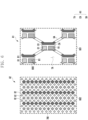
- FIG. 6 is a diagram illustrating a UDC area (e.g., a first area A1) and a normal area (e.g., a second area A2) other than the UDC area of a display according to various embodiments.
- a UDC area e.g., a first area A1
- a normal area e.g., a second area A2
- the pixel layer (e.g., the pixel layer 540 in FIG. 5 ) of the display 400 may have the first area A1 and the second area A2.
- the second area A2 may be an area that does not overlap with the angle of view of the UDC, and may be an area other than the first area A1.
- the UDC may have a designated angle of view.
- the first area A1 may be an area corresponding to the angle of view of the UDC
- the second area A2 may be an area not corresponding to the angle of view of the UDC.
- the first area A1 may include a cluster area CA that contains the plurality of first pixels 542 and the driving circuit (e.g., TFT) for driving the first pixels 542 and overlaps with at least a portion of the opaque mask (e.g., the opaque mask 521 in FIG. 5 ), a wiring area SA that connects the cluster areas CA, and/or a transmission area TA that is disposed between the cluster areas CA and does not overlap with the opaque mask 521.
- the driving circuit e.g., TFT
- the plurality of first pixels 542 may be arranged in the first area A1.
- the plurality of first pixels 542 are subpixels of a first type and may include a first subpixel R1 representing a first color (e.g., red), a second subpixel G1 representing a second color (e.g., green), and/or a third subpixel B1 representing a third color (e.g., blue).
- a first subpixel R1 representing a first color (e.g., red)
- a second subpixel G1 representing a second color (e.g., green)
- a third subpixel B1 representing a third color (e.g., blue).
- one first subpixel R1, one second subpixel G1, and one third subpixel B1 may be disposed adjacent to each other, thereby including one group.
- an area in which the first subpixel R1, the second subpixel G1, and the third subpixel B1 including one group are disposed may be referred to as the cluster area CA.
- a plurality of cluster areas CA may be disposed at intervals in the first area A1, and the first subpixel R1, the second subpixel G1, and the third subpixel B1 including one group may be disposed in each cluster area CA.
- an area in which the opaque mask 521 is not formed between the cluster areas CA of the first area A1 may be referred to as the transmission area TA.
- the transmission area TA may form a light path through which external light is introduced into the UDC.
- an area where the opaque mask 521 is formed between the cluster areas CA of the first area A1 may be referred to as the wiring area SA.
- at least one signal wire (not shown) for driving the plurality of first pixels 542 may be disposed in the wiring area SA.
- the plurality of second pixels 541 may be arranged in the second area A2.
- the plurality of second pixels 541 are subpixels of a second type and may include a first subpixel R2 representing a first color (e.g., red), a second subpixel G2 representing a second color (e.g., green), and/or a third subpixel B2 representing a third color (e.g., blue).
- the density at which the first pixels 542 are disposed may be lower than the density at which the second pixels 541 are disposed.
- the second pixels 541 may be more densely arranged than the first pixels 542.
- n subpixels of the first type e.g., the first subpixel R1, the second subpixel G1, and the third subpixel B1 may be arranged at intervals.
- m subpixels of the second type may be arranged at intervals.
- 'n' may be smaller than 'm'.
- the electronic device 300 may be designed such that each size of the pixels disposed in the first area A1 is greater than each size of the pixels disposed in the second area A2.
- a first pixel driving circuit 800 for driving the first pixel 542 and a second pixel driving circuit 700 for driving the second pixel 541 may be different in shape from each other.
- a driving TFT (DT) of a first type e.g., the first driving TFT (DT1) in FIG. 8
- a driving TFT (DT) of a second type e.g., the second driving TFT (DT2) in FIG. 7
- DT2 e.g., the second driving TFT (DT2) in FIG. 7
- the first driving TFT (DT1) may be configured to supply a first current to the first pixel 542.
- the second driving TFT (DT2) may be configured to supply a second current to the second pixel 541.
- the first driving TFT (DT1) may supply the first current higher than the second current to the first pixel 542 so as to make the luminance of the first pixel 542 higher than the luminance of the second pixel 541.
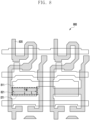
- FIG. 7 is a layout diagram illustrating a pixel driving circuit disposed in a normal area (e.g., a second area A2) of a display according to various embodiments.
- FIG. 8 is a layout diagram illustrating a pixel driving circuit disposed in a UDC area (e.g., a first area A1) of a display according to various embodiments.
- FIGS. 7 and 8 may be plan views illustrating at least a portion of the pixel layer 540 shown in FIG. 5 .
- the silicon layer (e.g., the silicon layer 530 in FIG. 5 ) of the display (e.g., the display 400 in FIG. 4 ) may include a semiconductor pattern 720 and a plurality of electrode patterns disposed to overlap with at least a portion of the semiconductor pattern 720.
- the semiconductor pattern 720 may include polysilicon or an oxide semiconductor. At least a portion of the semiconductor pattern 720 may include a channel region 721 doped with a p-type impurity (e.g., boron (B)) or an n-type impurity (e.g., phosphorus (P)), thereby forming a TFT.
- the plurality of electrode patterns may include at least one gate electrode pattern 711, at least one source electrode pattern (not shown), and/or at least one drain electrode pattern (not shown).
- the second area A2 includes the second pixel driving circuit 700 for driving the second pixel 541, and the second pixel driving circuit 700 may include the second driving TFT (DT2).
- the second driving TFT (DT2) may include a second gate electrode pattern 711 and a second channel region 721 disposed to overlap with at least a portion of the second gate electrode pattern 711.
- the second channel region 721 forming the second driving TFT (DT2) may have various curved shapes such as an English alphabet ⁇ reverse S', 'S', 'M', or 'W'.
- a symbol “W” in FIG. 7 may indicate a channel width of the second driving TFT (DT2).
- a symbol “L” in FIG. 7 may indicate a channel length of the second driving TFT (DT2).
- the silicon layer (e.g., the silicon layer 530 in FIG. 5 ) of the display (e.g., the display 400 in FIG. 4 ) may include a semiconductor pattern 820 and a plurality of electrode patterns disposed to overlap with at least a portion of the semiconductor pattern 820, and the plurality of electrode patterns may include a gate electrode pattern 811.
- the semiconductor pattern 820 shown in FIG. 8 may be formed on the same layer as the semiconductor pattern 720 shown in FIG. 7 .
- the first gate electrode pattern 811 shown in FIG. 8 may be formed on the same layer as the second gate electrode pattern 711 shown in FIG. 7 .
- the first area A1 includes the first pixel driving circuit 800 for driving the first pixel 542, and the first pixel driving circuit 800 may include the first driving TFT (DT1).
- the first driving TFT (DT1) may include a first gate electrode pattern 811 and a first channel region 821 disposed to overlap with at least a portion of the first gate electrode pattern 811.
- the first channel region 821 forming the first driving TFT (DT1) may have a straight shape that does not include a curved shape.
- the first channel region 821 forming the first driving TFT (DT1) does not have a curved shape such as an English alphabet 'reverse S', 'S', 'M', or ⁇ W'.
- the driving current supplied to the OLED from the driving TFT (DT) is proportional to the channel width (W) and inversely proportional to the channel length (L).
- the first driving TFT (DT1) may have an increased channel width (W) or a decreased channel length (L) as the first channel region 821 is formed to have a straight shape.
- the first channel width (W) of the first driving TFT (DT1) shown in FIG. 8 may be greater than the second channel width (W) of the second driving TFT (DT2) shown in FIG. 7 .
- the first channel length (L) of the first driving TFT (DT1) shown in FIG. 8 may be smaller than the second channel length (L) of the second driving TFT (DT2) shown in FIG. 7 .
- a distance between the TFTs (e.g., the first driving TFTs (DT1)) forming the first pixel driving circuit 800 shown in FIG. 8 may be smaller than a distance between the TFTs (e.g., the second driving TFTs (DT2)) forming the second pixel driving circuit 700 shown in FIG. 7 .
- the distance between the TFTs (e.g., the first driving TFTs (DT1)) forming the first pixel driving circuit 800 is designed to be relatively narrow, it is possible to reduce the area of the light-blocking area BA and increase the light transmittance in the first area overlapping with at least a portion of the UDC.
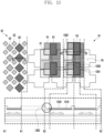
- the display according to various embodiments may be designed to enlarge the area of the anode and/or the organic layer of the OLED as shown in FIGS. 9 and 10 .
- FIG. 9 is a diagram illustrating a portion of a UDC area (e.g., a first area A1) of a display according to various embodiments.
- FIG. 10 is a cross-sectional view of a portion of a UDC area (e.g., a first area A1) of the display according to the embodiment shown in FIG. 9 .
- FIG. 10 may be a partial cross-sectional view showing a layered structure of the display according to an embodiment viewed from the line 10-10 of FIG. 9 .
- the first area A1 of the display may include a plurality of cluster areas CA in which a plurality of first pixels 542 are disposed, a wiring area SA connecting the plurality of cluster areas CA and having at least one signal wire (not shown) disposed, and a transmission area TA.
- the plurality of cluster areas CA and the wiring area SA may form a light-blocking area BA (e.g., the light-blocking area BA in FIG. 5 ) that overlaps with the opaque mask 521.
- a light-blocking area BA e.g., the light-blocking area BA in FIG. 5
- one first subpixel R1, one second subpixel G1, and one third subpixel B1 are disposed adjacently to form one group.
- the first pixels 542 may have extensions 911, 912, and 913 extending from the cluster area CAto a portion of the wiring area SA.
- the first subpixel R1, the second subpixel G1, and/or the third subpixel B1 are disposed in each cluster area CA, and the first subpixel R1, the second subpixel G1, and the third subpixel B1 may have the extensions 911, 912, and 913, respectively.
- the first subpixel R1 includes a first extension 911
- the first extension 911 may include a first anode (not shown) and a first organic layer (not shown) formed to extend from the cluster area CA to a portion of the wiring area SA adjacent to the first subpixel R1.
- the second sub-pixel G1 includes a second extension 912
- the second extension 912 may include a second anode (e.g., the second anode 1010 in FIG. 10 ) and a second organic layer (e.g., the second organic layer 1020 in FIG. 10 ) formed to extend from the cluster area CAto a portion of the wiring area SA adjacent to the second sub-pixel G1.
- a second anode e.g., the second anode 1010 in FIG. 10
- a second organic layer e.g., the second organic layer 1020 in FIG. 10
- the third sub-pixel B1 includes a third extension 913
- the third extension 913 may include a third anode (e.g., the third anode 1030 in FIG. 10 ) and a third organic layer (e.g., the third organic layer 1040 in FIG. 10 ) formed to extend from the cluster area CA to a portion of the wiring area SA adjacent to the third sub-pixel B1.
- a third anode e.g., the third anode 1030 in FIG. 10
- a third organic layer e.g., the third organic layer 1040 in FIG. 10
- the first extension 911 of the first subpixel R1 may be formed to have a first length 921.
- the second extension 912 of the second subpixel G1 may be formed to have a second length 922.
- the third extension 913 of the third sub-pixel B1 may be formed to have a third length 923.
- the first length 921, the second length 922, and the third length 923 may all be equal to each other.
- the first length 921, the second length 922, and the third length 923 may be different from each other.
- the width of the wiring area SA may be increased from a first width 931 to a second width 932 so as to increase the deposition area of the extensions 911, 912, and 913.
- the area of the transmission area TA may remain substantially unchanged or increase because the distance (e.g., pixel pitch) between the TFTs (e.g., the first driving TFTs (DT1)) forming the first pixel driving circuit 800 is reduced as described in FIG. 8 .
- the opaque mask 521 is formed to increase in width in the wiring area SA but decreases in width in the cluster area CA, the area of the transmission area TA may not substantially change or may increase.
- the wiring area SA may be formed to have the constant second width 932 between two adjacent cluster areas CA.
- the wiring area SA may have the same second width 932 in a portion where the extensions 911, 912, and 913 of the first pixel 542 are formed and in a portion where the extensions 911, 912, and 913 of the first pixel 542 are not formed.
- the wiring area SA may be formed to have the first width 931 or the second width 932 not constant between two adjacent cluster areas CA.
- the wiring area SA may have the relatively large second width 932 in a portion corresponding to the extension of the first pixel 542 and have the relatively small first width 931 in a portion where the extension of the first pixel 542 is not formed.
- the subpixels R1, G1, and B1 of the first area A1 are OLED-type subpixels and may include anodes 1010 and 1030 and organic layers 1020 and 1040 stacked on the anodes 1010 and 1010.
- FIG. 10 shows a portion of the second subpixel G1 and a portion of the third subpixel B1 disposed with the wiring area SA interposed therebetween.
- the second subpixel G1 may include the second anode 1010 and the second organic layer 1020 stacked on the second anode 1010. As shown, the second anode 1010 and the second organic layer 1020 may have a second extension 1001 (e.g., the second extension 912 in FIG. 9 ) extending partly into the wiring area SA, in addition to a portion formed within the cluster area CA.
- a second extension 1001 e.g., the second extension 912 in FIG. 9
- the third subpixel B1 may include the third anode 1030 and the third organic layer 1040 stacked on the third anode 1030.
- the first subpixel R1 may include a first anode and a first organic layer stacked on the first anode.
- the first anode and the first organic layer of the first subpixel R1 may have a first extension (e.g., the first extension 911 in FIG. 9 ) extending partly into the wiring area SA.
- the third anode and the third organic layer of the third subpixel B1 similarly to the second extension of FIG. 10 , have a third extension (e.g., the third extension 913 in FIG. 9 ) extending partly into the wiring area SA.
- the display includes the extension 1001 that the first pixel 542 disposed in the first area A1 extends to the wiring area SA, thereby reducing the lifespan or burn-in difference between the first pixel 542 and the second pixel 541 that may occur when the first driving TFT (DT1) of the first area A1 and the second driving TFT (DT2) of the second area A2 have different structures.
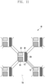
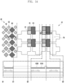
- FIG. 11 is a diagram illustrating a portion of a UDC area (e.g., a first area A1) of a display according to a comparative example.
- FIG. 12 is a cross-sectional view of a portion of the UDC area (e.g., a first area A1) of the display according to the comparative example shown in FIG. 11 .
- FIG. 12 may be a partial cross-sectional view of the display according to the comparative example viewed from the line 12-12 of FIG. 11 .
- the first pixels 542 may not have extensions (e.g., the extensions 911, 912, and 913 in FIG. 9 ).
- the first subpixel R1, the second subpixel G1, and/or the third subpixel B1 of the first pixels 542 may be disposed in the cluster area CA and may not be formed in the wiring area SA.
- the display according to the comparative example shown in FIGS. 11 and 12 may have an increased lifespan or burn-in difference between the first pixel 542 and the second pixel 541 when the first driving TFT (DT1) of the first area A1 and the second driving TFT (DT2) of the second area A2 have different structures.
- FIG. 13 is a diagram illustrating a UDC area (e.g., a first area A1) and a normal area (e.g., a second area A2) other than the UDC area of a display according to various embodiments, and a cross-sectional view taken along lines K1-K1 and K2-K2.
- FIG. 14 is a diagram illustrating a UDC area (e.g., a first area A1) and a normal area (e.g., a second area A2) other than the UDC area of a display according to a comparative example, and a cross-sectional view taken along lines Q1-Q1 and Q2-Q2.
- the display may include transparent light-emitting portions 1301, 1302, and 1303 in which the first pixels 542 disposed in the first area A1 extend partly into the transmission area TA.
- the transparent light-emitting portions 1301, 1302, and 1303 may be configured to include an anode 1310 including a transparent anode (e.g., the lower transparent electrode 1621 and/or the upper transparent electrode 1623 in FIG. 16 ) and an organic layer 1320 (e.g., the second portion 1632 of the organic layer 1630 in FIG. 16 ) stacked on the anode 1310.
- the first pixel 542 may not include the transparent light-emitting portions 1301, 1302, and 1303.
- each of the first subpixel R1, the second subpixel G1, and/or the third subpixels B1 of the first pixels 542 disposed in the first area A1 may include the anode 1310 and the organic layer 1320 stacked on the anode 1310.
- each of the first subpixel R1, the second subpixel G1, and/or the third subpixel B1 may include the transparent light-emitting portions 1301, 1302, and 1303 extending partly into the transmission area TA.
- the transparent light-emitting portions 1301, 1302, and 1303 may include the anode 1310 made of a transparent material and the organic layer 1320 stacked on the anode 1310.
- the transparent light-emitting portions 1301, 1302, and 1303 will be described in detail.
- the first subpixel R1 may include a first anode disposed to correspond to the cluster area CA, and a first organic layer stacked on the first anode.
- the first anode of the first subpixel R1 may have a structure in which at least one opaque electrode (e.g., Ag) and at least one transparent electrode (e.g., indium tin oxide (ITO)) are stacked.
- the at least one transparent electrode of the first anode may be formed to correspond to the cluster area CA and extend from the cluster area CA to a portion of the transmission area TA. In the first anode, the transparent electrode formed to extend partly into the transmission area TA may be referred to as a first transparent anode.
- the first organic layer stacked on the first anode extends partly into the transmission area TA to cover the first transparent anode, thereby forming a first transparent light-emitting portion 1301.
- the first transparent light-emitting portion 1301 may include the first transparent anode and the first organic layer covering the first transparent anode.
- the first transparent light-emitting portion 1301 is an area through which light can pass, and can provide an effect of improving transmittance and expanding a light-emitting area by outputting light of a designated color (e.g., red).
- the second subpixel G1 may include a second anode disposed to correspond to the cluster area CA, and a second organic layer stacked on the second anode.
- the second anode of the second subpixel G1 may have a structure in which at least one opaque electrode and at least one transparent electrode are stacked.
- the at least one transparent electrode of the second anode may be formed to correspond to the cluster area CA and extend from the cluster area CAto a portion of the transmission area TA.
- the transparent electrode formed to extend partly into the transmission area TA may be referred to as a second transparent anode.
- the second organic layer stacked on the second anode extends partly into the transmission area TA to cover the second transparent anode, thereby forming a second transparent light-emitting portion 1302.
- the second transparent light-emitting portion 1302 may include the second transparent anode and the second organic layer covering the second transparent anode.
- the second transparent light-emitting portion 1302 is an area through which light can pass, and can provide an effect of improving transmittance and expanding a light-emitting area by outputting light of a designated color (e.g., green).
- the third subpixel B1 may include a third anode disposed to correspond to the cluster area CA, and a third organic layer stacked on the third anode.
- the third anode of the third subpixel B1 may have a structure in which at least one opaque electrode and at least one transparent electrode are stacked.
- the at least one transparent electrode of the third anode may be formed to correspond to the cluster area CA and extend from the cluster area CA to a portion of the transmission area TA.
- the transparent electrode formed to extend partly into the transmission area TA may be referred to as a third transparent anode.
- the third organic layer stacked on the third anode extends partly into the transmission area TA to cover the third transparent anode, thereby forming a third transparent light-emitting portion 1303.
- the third transparent light-emitting portion 1303 may include the third transparent anode and the third organic layer covering the third transparent anode.
- the third transparent light-emitting portion 1303 is an area through which light can pass, and can provide an effect of improving transmittance and expanding a light-emitting area by outputting light of a designated color (e.g., blue).
- the pixel density of the first area A1 is lowered, thereby reducing the phenomenon in which the lattice structure is visually recognized by the user. Also, by forming the transparent light-emitting portions 1301, 1302, and 1303 in the first area A1, the light emitting area can be expanded.
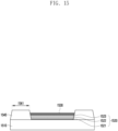
- FIG. 15 is a cross-sectional view illustrating a stacked structure of a pixel disposed in a normal area (e.g., a second area A2) of a display according to various embodiments.
- FIG. 15 may be a cross-sectional view illustrating a stacked structure of any one pixel disposed in the normal area (e.g., the second area A2) shown in FIG. 13 .
- FIG. 16 is a cross-sectional view illustrating a stacked structure of a pixel disposed in a UDC area (e.g., a first area A1) of a display according to various embodiments.
- FIG. 16 may be a cross-sectional view illustrating a stacked structure of a pixel disposed in the UDC area (e.g., the first area A1) shown in FIG. 13 .
- the second pixel (e.g., the second pixel 541 in FIG. 5 ) disposed in the second area A2 of the display includes an OLED, and the OLED may include an anode 1520, an organic layer 1530 stacked on the anode 1520, and a cathode (not shown) stacked on the organic layer 1530.
- the anode 1520 and the organic layer 1530 may be formed on an insulating layer 1510 (e.g., the substrate 511 in FIG. 5 ).
- the anode 1520 and the organic layer 1530 may be partitioned by a pixel definition layer (PDL) 1540.
- the pixel definition layer 1540 may form a boundary between adjacent subpixels.
- the pixel definition layer 1540 formed between two adjacent subpixels in the second area A2 may have a third width 1541.
- the anode 1520 formed in the second area A2 may have a structure in which at least one opaque electrode 1522 and at least one transparent electrode 1521 and 1523 are stacked.
- the opaque electrode 1522 may include, but is not limited to, an Ag material.
- the transparent electrodes 1521 and 1523 may include, but is not limited to, indium tin oxide (ITO).
- the anode 1520 formed in the second area A2 may include a lower transparent electrode 1521 formed on the insulating layer 1510, the opaque electrode 1522 formed on the lower transparent electrode 1521, and/or an upper transparent electrode 1523 formed on the opaque electrode 1522.
- the first pixel (e.g., the first pixel 542 in FIG. 5 ) disposed in the first area A1 of the display (e.g., the display 400 in FIG. 4 ) includes an OLED, and the OLED may include an anode 1620, an organic layer 1630 stacked on the anode 1620, and a cathode (not shown) stacked on the organic layer 1630.
- the anode 1620 and the organic layer 1630 may be formed on an insulating layer 1610 (e.g., the substrate 511 in FIG. 5 ).
- the anode 1620 and the organic layer 1630 may be partitioned by a pixel definition layer (PDL) 1640.
- PDL pixel definition layer
- the pixel definition layer 1640 may form a boundary between adjacent subpixels.
- the pixel definition layer 1640 formed between two adjacent subpixels in the first area A1 may have a fourth width 1641.
- the fourth width 1641 may be smaller than the third width 1541 described with reference to FIG. 15 .
- the fourth width 1641 is smaller than the third width 1541, it is possible to increase the area of the transmission area of the first area A1 (e.g., the transmission area TA in FIG. 5 ) and increase the light transmittance of the first area A1.
- the anode 1620 formed in the first area A1 may have a structure in which at least one opaque electrode 1622 and at least one transparent electrode 1621 and 1623 are stacked.
- the opaque electrode 1622 may include, but is not limited to, an Ag material.
- the transparent electrodes 1621 and 1623 may include, but is not limited to, indium tin oxide (ITO).
- the anode 1620 formed in the first area A1 may include a lower transparent electrode 1621 formed on the insulating layer 1610, the opaque electrode 1622 formed on the lower transparent electrode 1621, and/or an upper transparent electrode 1623 formed on the opaque electrode 1622.
- At least one layer of the lower transparent electrode 1621 and the upper transparent electrode 1623 of the anode 1620 formed in the first are A1 may extend toward the pixel definition layer 1640 and form the transparent light-emitting portions 1301, 1302, and 1303 described with reference to FIG. 13 .
- the upper transparent electrode 1623 and/or the lower transparent electrode 1621 may extend partly into the transmission area TA.
- the organic layer 1630 formed in the first area A1 is disposed to cover the extension of the lower transparent electrode 1621 (or the extensions of the upper transparent electrode 1623 and the lower transparent electrode 1621 or the extension of the upper transparent electrode 1623) adjacent to the pixel definition layer 1640, thereby forming the transparent light-emitting portions 1301, 1302, and 1303.
- the organic layer 1630 formed in the first area A1 may include a first portion 1631 overlapping a portion of the anode 1620 including the opaque electrode 1622, and a second portion 1632 disposed outside the first portion 1631 and overlapping with the at least one transparent electrode 1621 and 1623 that is the extension of the anode 1620.
- FIG. 16 shows that both the lower transparent electrode 1621 and the upper transparent electrode 1623 extend outward to form the transparent light-emitting portions 1301, 1302, and 1303, but this is not a limitation.
- only the lower transparent electrode 1621 or only the upper transparent electrode 1623 may extend outward to form the transparent light-emitting portions 1301, 1302, and 1303.
- FIG. 17 is a cross-sectional view illustrating a stacked structure of a pixel disposed in a UDC area (e.g., a first area A1) of a display according to various embodiments.
- FIG. 17 may be a cross-sectional view illustrating a stacked structure of any one pixel disposed in the UDC area (e.g., the first area A1) shown in FIG. 13 .
- the display shown in FIG. 17 may be similar at least in part to the display shown in FIG. 16 or include various embodiments. In the following description, only different components in FIG. 17 will be described, and unexplained features will be replaced with the description of FIG. 16 .
- At least one layer of the lower transparent electrode 1621 and the upper transparent electrode 1623 of the anode 1620 formed in the first are A1 may extend toward the pixel definition layer 1640 and form the transparent light-emitting portions 1301, 1302, and 1303 described with reference to FIG. 13 .
- the display shown in FIG. 17 may have a structure for compensating for a step difference formed as only some electrode layers (e.g., the lower transparent electrode 1621 and/or the upper transparent electrode 1623) extend outward among the plurality of electrode layers including the anode 1620.
- a thickness 1711 of the first portion 1631 and a thickness 1712 of the second portion 1632 may be formed differently.
- the organic layer 1630 may be formed such that the thickness 1712 of the second portion 1632 is greater than the thickness 1711 of the first portion 1631. Therefore, in the organic layer 1630, the upper surface of the first portion 1631 and the upper surface of the second portion 1632 may have substantially the same height.
- FIG. 18 is a cross-sectional view illustrating a stacked structure of a pixel disposed in a UDC area (e.g., a first area A1) of a display according to various embodiments.
- FIG. 18 may be a cross-sectional view illustrating a stacked structure of any one pixel disposed in the UDC area (e.g., the first area A1) shown in FIG. 13 .
- the display shown in FIG. 18 may be similar at least in part to the display shown in FIG. 16 or include various embodiments. In the following description, only different components in FIG. 18 will be described, and unexplained features will be replaced with the description of FIG. 16 .
- the display (e.g., the display 400 in FIG. 4 ) shown in FIG. 18 may have a structure for compensating for a step difference formed as only some electrode layers (e.g., the lower transparent electrode 1621 and/or the upper transparent electrode 1623) extend outward among the plurality of electrode layers 1621, 1622, and 1623 including the anode 1620.
- the display of this embodiment may further include a buffer layer 1811, and the buffer layer 1811 may be disposed to compensate for such a step difference.
- the buffer layer 1811 may be formed in an outer region of the anode 1620 adjacent to the pixel definition layer 1640. As the buffer layer 1811 is formed, the upper surface of the first portion 1631 and the upper surface of the second portion 1632 in the organic layer 1630 may have substantially the same height.
- the display according to various embodiments may have a viewing angle control structure for differently designing a viewing angle of the first area A1 and a viewing angle of the second area A2.
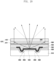
- the viewing angle control structure may include a method using a refraction control film 1970 formed on the OLED and/or a method using a shape change of the anode 1920 in the first area A1.
- the display having the viewing angle control structure can reduce a phenomenon in which a grid-shaped structure is visually recognized by a user in the first area A1.
- the display further including the viewing angle control structures according to various embodiments will be described with reference to FIGS. 19 to 22 .
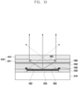
- FIG. 19 is a cross-sectional view illustrating a viewing angle design structure of a pixel disposed in a normal area (e.g., a second area A2) of a display according to various embodiments.
- FIG. 19 may be a cross-sectional view illustrating a stacked structure of any one pixel disposed in the normal area (e.g., the second area A2) shown in FIG. 13 .
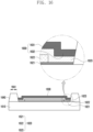
- FIG. 20 is a cross-sectional view illustrating a viewing angle design structure of a pixel disposed in a UDC area (e.g., a first area) of a display according to an embodiment.
- FIG. 20 may be a cross-sectional view illustrating a stacked structure of any one pixel disposed in the UDC area (e.g., the first area A1) shown in FIG. 13 .
- the second pixel 541 disposed in the second area A2 of the display includes an OLED
- the OLED may include an anode 1920, an organic layer 1940 stacked on the anode 1920, and a cathode (not shown) stacked on the organic layer 1940.
- the anode 1920 and the organic layer 1940 may be formed on an insulating layer 1910 (e.g., the substrate 511 in FIG. 5 ).
- the anode 1920 and the organic layer 1940 may be partitioned by a pixel definition layer (PDL) 1930.
- the pixel definition layer 1930 may form a boundary between adjacent subpixels.
- encapsulation layers 1950 and 1960 may be formed on the OLED including the anode 1920 and the organic layer 1940.
- the encapsulation layers 1950 and 1960 may include an organic encapsulation layer 1950 (e.g., the organic encapsulation layer 550 in FIG. 5 , thin film encapsulation (TFE)) made of an organic material, or an inorganic encapsulation layer 1960 made of an inorganic material.
- a refraction control film 1970 may be formed on the encapsulation layers 1950 and 1960.
- the refraction control film 1970 may include a touch sensor layer 1971 (e.g., the touch panel 432 in FIG.
- passivation e.g., YPVX
- MLP micro light control pattern
- the refraction control film 1970 may control the refractive index of light by adjusting a gap of the passivation (e.g., YPVX) for the touch electrode in the touch sensor layer 1971.
- the touch sensor layer 1971 may have an opening that overlaps with at least a portion of the anode 1920 and has a fifth width 1901 through gap adjustment of the passivation for the touch electrode.
- the MLP structure 1972 of the refraction control film 1970 may be formed of a high refractive index film and may have, for example, a higher refractive index (e.g., about a refractive index of 1.6) than a refractive index (e.g., about a refractive index of about 1.5) of the opening of the passivation (e.g., YPVX) for the touch electrode.
- the MLP structure 1972 may include a plurality of layers (not shown) having different refractive indices and may have a structure in which an optical path is changed using a difference in refractive index between materials including the plurality of layers.
- the second area A2 may have a first viewing angle 1902 that is relatively narrower than that of the first area A1 through refractive index control using the refraction control film 1970.
- the first area A1 of the display may include the refraction control film 1970, and the refraction control film 1970 may include the touch sensor layer 1971 (e.g., the touch panel 432 in FIG. 4 ) having the passivation (e.g., YPVX) for the touch electrode, and the MLP structure 1972 (e.g., a material or light path control film having a certain transmittance and thickness between the OLED and the polarization layer).
- the touch sensor layer 1971 e.g., the touch panel 432 in FIG. 4
- the passivation e.g., YPVX
- MLP structure 1972 e.g., a material or light path control film having a certain transmittance and thickness between the OLED and the polarization layer.
- the refraction control film 1970 may control the refractive index of light by adjusting a gap of the passivation (e.g., YPVX) for the touch electrode in the touch sensor layer 1971.
- the touch sensor layer 1971 may have an opening having a sixth width 2001 through gap adjustment of the passivation for the touch electrode.
- the sixth width 2001 may be greater than the fifth width 1901 described with reference to FIG. 19 .
- the MLP structure 1972 of the refraction control film 1970 may be formed of a low refractive index film and may have, for example, a lower refractive index than a refractive index (e.g., about a refractive index of about 1.5) of the opening of the passivation (e.g., YPVX) for the touch electrode.
- a refractive index e.g., about a refractive index of about 1.5
- the opening of the passivation e.g., YPVX
- the anode 1920 in the first area A1 may have at least one curved surface, unlike the anode 1920 in the second area A2 having a flat film shape.
- the anode 1920 of the first area A1 may have a concave portion 2003 at the periphery of the anode 1920 adj acent to the pixel definition layer (PDL) 1930.
- the surface of the concave portion 2003 may have a concave curved surface and be connected to a side surface of the pixel definition layer 1930.
- the height of the surface of the concave portion 2003 may be lower than that of the central region of the anode 1920.
- the first area A1 of the display may have a second viewing angle 2002, which is a relatively wide viewing angle than the second area A2, through a change in the design of the refraction control film 1970 and a change in the shape of the anode 1920 of the first area A1.
- the shape of the concave portion 2003 may be variously changed or modified as shown in FIGS. 21 and 22 . According to various embodiments, the shape of the concave portion 2003 may not be limited to the shapes shown in FIGS. 20 , 21 and 22 .
- FIG. 21 is a cross-sectional view illustrating a viewing angle design structure of a pixel disposed in a UDC area (e.g., a first area A1) of a display according to various embodiments.
- FIG. 22 is a cross-sectional view schematically a viewing angle design structure of a pixel disposed in a UDC area (e.g., a first area A1) of a display according to various embodiments.
- FIGS. 21 and 22 may be cross-sectional views illustrating a stacked structure of any one pixel disposed in the UDC area (e.g., the first area A1) shown in FIG. 13 .
- FIGS. 21 and 22 may be similar at least in part to the display shown in FIG. 20 or include various embodiments. In the following description, only different components in FIGS. 21 and 22 will be described, and unexplained features will be replaced with the description of FIG. 20 .
- the anode 1920 in the first area A1 may have a curved surface including a plurality of irregularities 2103, unlike the anode 1920 in the second area A2 having a flat film shape.
- the anode 1920 of the first area A1 may have the curved surface including the plurality of irregularities 2103 over the entire area between the pixel definition layers (PDL) 1930.
- the first area A1 of the display according to this embodiment may have a third viewing angle 2102, which is a relatively wide viewing angle than the second area A2, through a change in the design of the refraction control film 1970 and a change in the shape of the anode 1920 of the first area A1.
- Reference numeral "2101" in FIG. 21 denotes a gap of passivation (e.g., YPVX) for a touch electrode, and this gap may be greater than the fifth width 1901 described with reference to FIG. 19 .
- the anode 1920 in the first area A1 may have a single curved surface 2203 whose height decreases toward the center of the anode 1920, unlike the anode 1920 in the second area A2 having a flat film shape.
- the anode 1920 of the first area A1 may have the highest height in a portion adjacent to the pixel definition layer (PDL) 1930 and have the lowest height in a central portion of the anode 1920.
- PDL pixel definition layer
- the first area A1 of the display according to this embodiment may have a fourth viewing angle 2202, which is a relatively wide viewing angle than the second area A2, through a change in the design of the refraction control film 1970 and a change in the shape of the anode 1920 of the first area A1.
- Reference numeral "2201" in FIG. 22 denotes a gap of passivation (e.g., YPVX) for a touch electrode, and this gap may be greater than the fifth width 1901 described with reference to FIG. 19 .
- the driving circuit e.g., the driving TFT
- the driving circuit for driving the first pixel 542 is not disposed in the first area A1
- the first pixel 542 disposed in the first area A1 may be driven by a driving circuit disposed in the second area A2.
- the driving circuit for driving the first pixel 542 when the driving circuit for driving the first pixel 542 is not disposed in the first area A1, the first pixel 542 disposed in the first area A1 may be driven by a driving circuit (not shown) disposed between the first area A1 and the second area A2.
- the driving circuit for driving the first pixel 542 when the driving circuit for driving the first pixel 542 is not disposed in the first area A1, the pixels disposed in the first area A1 may be driven by a driving circuit (not shown) disposed in the second area A2 to drive the pixels disposed in the second area A2.
- one driving circuit (not shown) disposed in the second area A2 not only drives the second pixel 541 disposed in the second area A2, but also drives the first pixel 542 disposed in the first area A1.
- the driving circuit is capable of driving the red pixel (not shown) in the first area A1 as well as the red pixel in the second area A2.
- an electronic device e.g., the electronic device 100 in FIG. 1
- the display 101 may include a first area (e.g., the first area A1 in FIG. 5 ) in which a first pixel (e.g., the first pixel 542 in FIG.
- the first pixel driving circuit 800 may include a first driving thin film transistor (TFT) (e.g., the first driving TFT (DT1) in FIG.
- the second pixel driving circuit 700 may include a second driving TFT (e.g., the second driving TFT (DT2) in FIG. 7 ) having a second channel region of a curved shape.
- a first channel width of the first driving TFT (DT1) may be greater than a second channel width of the second driving TFT (DT2), and a first channel length of the first driving TFT (DT1) may be less than a second channel length of the second driving TFT (DT2).
- the first area A1 may include a cluster area (e.g., the cluster area CA in FIG. 9 ) in which the first pixel 542 and the first pixel driving circuit 800 are disposed to overlap with each other, a wiring area (e.g., the wiring area SA in FIG. 9 ) connecting the cluster areas CA adjacent to each other and in which at least one signal wire is disposed, and a transmission area (e.g., the transmission area TA in FIG. 9 ) other than the cluster area CA and the wiring area SA. At least a portion of the first pixel 542 may extend partly into the wiring area SA.
- the first pixel 542 may include a first subpixel (e.g., the first subpixel R1 in FIG. 9 ), a second subpixel (e.g., the second subpixel G1 in FIG. 9 ), and a third subpixel (e.g., the third subpixel B1 in FIG. 9 ), wherein the first subpixel R1, the second subpixel G1, and the third subpixel B1 may be arranged to form one group in the one cluster area CA.
- Each of the first subpixel R1, the second subpixel G1, and the third subpixel B1 may have an extension extending from the one cluster area CAto a portion of the wiring area SA.
- the first subpixel R1 may have a first extension 911 extending to a portion of the wiring area SA adjacent to the first subpixel R1
- the second subpixel G1 may have a second extension 912 extending to a portion of the wiring area SA adj acent to the second subpixel G1
- the third subpixel B1 may have a third extension 913 extending to a portion of the wiring area SA adjacent to the third subpixel B1.
- the first extension 911 may include a first anode and a first organic layer formed to extend from a portion of the cluster area CA to a portion of the wiring area SA
- the second extension 912 may include a second anode and a second organic layer formed to extend from a portion of the cluster area CAto a portion of the wiring area SA
- the third extension 913 may include a third anode and a third organic layer formed to extend from a portion of the cluster area CA to a portion of the wiring area SA.
- the first extension 911 may have a first length
- the second extension 912 may have a second length
- the third extension 913 may have a third length.
- the first length, the second length, and the third length may be all equal to each other.
- the first extension 911 may have a first length
- the second extension 912 may have a second length
- the third extension 913 may have a third length.
- the first length, the second length, and the third length may be different from each other.
- the wiring area SA may have a first width in a portion where the extension is not formed, and have a second width greater than the first width in a portion where the extension is formed.
- the wiring area SA may have a constant width in a portion where the extension is not formed and a portion where the extension is formed.
- the first pixel 542 may include an organic light emitting diodes (OLED) including an anode, an organic layer stacked on the anode, and a cathode stacked on the anode.
- OLED organic light emitting diodes
- the anode may have a structure in which at least one transparent electrode and at least one opaque electrode are stacked, and the OLED may include a transparent light-emitting portion formed by a portion of the transparent electrode and a portion of the organic layer, which extend to a portion of the transmission area TA.
- the anode may include a lower transparent electrode formed on an insulating layer, an opaque electrode formed on the lower transparent electrode, and an upper transparent electrode formed on the opaque electrode.
- the transparent light-emitting portion of the OELD may include a portion of the lower transparent electrode extending to a portion of the transmission area TA and a portion of the organic layer covering the extending portion of the lower transparent electrode.
- the transparent light-emitting portion of the OELD may include a portion of the upper transparent electrode extending to a portion of the transmission area TA and a portion of the organic layer covering the extending portion of the upper transparent electrode.
- the transparent light-emitting portion of the OELD may include a portion of the lower and upper transparent electrodes extending to a portion of the transmission area TA and a portion of the organic layer covering the extending portion of the upper transparent electrode.
- the organic layer may include a first portion overlapping with at least a portion of the opaque electrode to correspond to the cluster area CA, and a second portion overlapping with the transparent electrode in the transparent light-emitting portion outside the first portion.
- the first portion of the organic layer may have a first thickness
- the second portion of the organic layer may have a second thickness greater than the first thickness configured to compensate for a height step difference between the first portion and the second portion.
- the first pixel 542 may include a transparent buffer layer formed between the second portion and the transparent electrode configured to compensate for a height step difference between the first portion and the second portion.
- a refraction control film may be disposed on the OELD.
- the refraction control film may be formed to have a designated first refractive index
- the refraction control film may be formed to have a designated second refractive index higher than the first refractive index.
- the refraction control film in the second area A2, may have an opening having a designated third width, and in the first area A1, the refraction control film may have an opening having a designated fourth width greater than the third width.
- the anode of the OLED may have at least one curved surface.
Landscapes
- Physics & Mathematics (AREA)
- Engineering & Computer Science (AREA)
- Optics & Photonics (AREA)
- Microelectronics & Electronic Packaging (AREA)
- Geometry (AREA)
- Inorganic Chemistry (AREA)
- Chemical & Material Sciences (AREA)
- Life Sciences & Earth Sciences (AREA)
- Sustainable Development (AREA)
- Computer Hardware Design (AREA)
- General Physics & Mathematics (AREA)
- Theoretical Computer Science (AREA)
- Devices For Indicating Variable Information By Combining Individual Elements (AREA)
Applications Claiming Priority (2)
| Application Number | Priority Date | Filing Date | Title |
|---|---|---|---|
| KR1020220049076A KR20230149626A (ko) | 2022-04-20 | 2022-04-20 | Udc를 포함한 전자 장치 |
| PCT/KR2023/004389 WO2023204481A1 (fr) | 2022-04-20 | 2023-03-31 | Dispositif électronique comprenant une caméra udc |
Publications (3)
| Publication Number | Publication Date |
|---|---|
| EP4482279A1 true EP4482279A1 (fr) | 2024-12-25 |
| EP4482279A4 EP4482279A4 (fr) | 2025-06-25 |
| EP4482279B1 EP4482279B1 (fr) | 2026-03-25 |
Family
ID=88415171
Family Applications (1)
| Application Number | Title | Priority Date | Filing Date |
|---|---|---|---|
| EP23792061.6A Active EP4482279B1 (fr) | 2022-04-20 | 2023-03-31 | Dispositif électronique comprenant une caméra udc |
Country Status (2)
| Country | Link |
|---|---|
| US (1) | US12063831B2 (fr) |
| EP (1) | EP4482279B1 (fr) |
Family Cites Families (12)
| Publication number | Priority date | Publication date | Assignee | Title |
|---|---|---|---|---|
| TWI452502B (zh) * | 2011-12-16 | 2014-09-11 | Au Optronics Corp | 觸控畫素陣列基板、觸控顯示面板與觸控畫素結構 |
| CN110660823A (zh) | 2018-06-29 | 2020-01-07 | 京东方科技集团股份有限公司 | 显示基板、其显示方法、显示装置及高精度金属掩模板 |
| KR102770831B1 (ko) | 2019-02-07 | 2025-02-24 | 삼성디스플레이 주식회사 | 표시 장치 |
| KR102896749B1 (ko) * | 2019-02-21 | 2025-12-05 | 삼성디스플레이 주식회사 | 표시 장치 및 표시 장치의 제조방법 |
| KR102814726B1 (ko) * | 2019-03-28 | 2025-05-30 | 삼성디스플레이 주식회사 | 표시 장치 |
| KR20200136549A (ko) | 2019-05-27 | 2020-12-08 | 삼성디스플레이 주식회사 | 표시 장치 및 표시 장치의 제조 방법 |
| KR102707313B1 (ko) | 2019-08-01 | 2024-09-19 | 삼성디스플레이 주식회사 | 표시 장치 |
| KR20210059091A (ko) | 2019-11-13 | 2021-05-25 | 삼성디스플레이 주식회사 | 표시 장치 |
| KR102933157B1 (ko) | 2020-06-30 | 2026-03-03 | 엘지디스플레이 주식회사 | 표시 패널 및 이를 포함하는 표시 장치 |
| JP7576938B2 (ja) | 2020-07-22 | 2024-11-01 | 武漢天馬微電子有限公司 | 表示装置 |
| KR102929185B1 (ko) | 2020-10-06 | 2026-02-23 | 엘지디스플레이 주식회사 | 디스플레이 장치 |
| CN112259602B (zh) | 2020-10-10 | 2022-10-04 | 武汉华星光电半导体显示技术有限公司 | 一种小尺寸tft及显示面板 |
-
2023
- 2023-03-31 EP EP23792061.6A patent/EP4482279B1/fr active Active
- 2023-04-11 US US18/298,599 patent/US12063831B2/en active Active
Also Published As
| Publication number | Publication date |
|---|---|
| EP4482279B1 (fr) | 2026-03-25 |
| EP4482279A4 (fr) | 2025-06-25 |
| US12063831B2 (en) | 2024-08-13 |
| US20230345779A1 (en) | 2023-10-26 |
Similar Documents
| Publication | Publication Date | Title |
|---|---|---|
| US11930685B2 (en) | Electronic device including display and camera | |
| EP4005192B1 (fr) | Dispositif électronique comprenant un dispositif d'affichage et un dispositif de caméra | |
| EP3719610B1 (fr) | Dispositif électronique comprenant un affichage | |
| US11503749B2 (en) | Display including shielding member arranged to cover at least part of display driving circuit, and electronic device including same | |
| US11930686B2 (en) | Electronic device including camera module | |
| CN112289178B (zh) | 显示装置 | |
| US11017199B2 (en) | Display device with integrated sensor opening | |
| KR20190025798A (ko) | 입력감지유닛 및 이를 구비한 표시장치 | |
| EP3996359B1 (fr) | Dispositif électronique comprenant un module de caméra | |
| JP2024521239A (ja) | カメラモジュールを含む電子装置 | |
| US11251256B2 (en) | Display apparatus | |
| EP3913462B1 (fr) | Appareil électronique | |
| KR102632927B1 (ko) | 표시 장치 | |
| EP4369891B1 (fr) | Dispositif électronique comprenant un udc | |
| KR20230149626A (ko) | Udc를 포함한 전자 장치 | |
| EP4482279B1 (fr) | Dispositif électronique comprenant une caméra udc | |
| KR20230099119A (ko) | 표시 모듈 및 표시 장치 | |
| EP4284146B1 (fr) | Dispositif d'affichage | |
| EP4290577A1 (fr) | Appareil électronique comprenant un dispositif d'affichage | |
| KR20230024192A (ko) | Udc를 포함한 전자 장치 | |
| US20240381734A1 (en) | Display device | |
| KR20250042260A (ko) | 발광 표시 장치 | |
| KR20240108931A (ko) | 표시 장치 |
Legal Events
| Date | Code | Title | Description |
|---|---|---|---|
| STAA | Information on the status of an ep patent application or granted ep patent |
Free format text: STATUS: THE INTERNATIONAL PUBLICATION HAS BEEN MADE |
|
| PUAI | Public reference made under article 153(3) epc to a published international application that has entered the european phase |
Free format text: ORIGINAL CODE: 0009012 |
|
| STAA | Information on the status of an ep patent application or granted ep patent |
Free format text: STATUS: REQUEST FOR EXAMINATION WAS MADE |
|
| 17P | Request for examination filed |
Effective date: 20240918 |
|
| AK | Designated contracting states |
Kind code of ref document: A1 Designated state(s): AL AT BE BG CH CY CZ DE DK EE ES FI FR GB GR HR HU IE IS IT LI LT LU LV MC ME MK MT NL NO PL PT RO RS SE SI SK SM TR |
|
| A4 | Supplementary search report drawn up and despatched |
Effective date: 20250523 |
|
| RIC1 | Information provided on ipc code assigned before grant |
Ipc: H10D 86/40 20250101ALI20250519BHEP Ipc: H10K 50/858 20230101ALI20250519BHEP Ipc: H10K 59/124 20230101ALI20250519BHEP Ipc: H10K 50/11 20230101ALI20250519BHEP Ipc: H10K 50/816 20230101ALI20250519BHEP Ipc: H10K 50/813 20230101ALI20250519BHEP Ipc: H10K 59/131 20230101ALI20250519BHEP Ipc: H10K 59/35 20230101ALI20250519BHEP Ipc: H10K 59/121 20230101ALI20250519BHEP Ipc: H10K 59/65 20230101AFI20250519BHEP |
|
| DAV | Request for validation of the european patent (deleted) | ||
| DAX | Request for extension of the european patent (deleted) | ||
| GRAP | Despatch of communication of intention to grant a patent |
Free format text: ORIGINAL CODE: EPIDOSNIGR1 |
|
| STAA | Information on the status of an ep patent application or granted ep patent |
Free format text: STATUS: GRANT OF PATENT IS INTENDED |
|
| RIC1 | Information provided on ipc code assigned before grant |
Ipc: H10K 59/65 20230101AFI20250924BHEP Ipc: H10K 59/121 20230101ALI20250924BHEP Ipc: H10K 59/35 20230101ALI20250924BHEP Ipc: H10K 59/131 20230101ALI20250924BHEP Ipc: H10K 50/813 20230101ALI20250924BHEP Ipc: H10K 50/816 20230101ALI20250924BHEP Ipc: H10K 50/11 20230101ALI20250924BHEP Ipc: H10K 59/124 20230101ALI20250924BHEP Ipc: H10K 50/858 20230101ALI20250924BHEP Ipc: H10D 86/40 20250101ALI20250924BHEP |
|
| INTG | Intention to grant announced |
Effective date: 20251022 |
|
| GRAS | Grant fee paid |
Free format text: ORIGINAL CODE: EPIDOSNIGR3 |
|
| GRAA | (expected) grant |
Free format text: ORIGINAL CODE: 0009210 |
|
| STAA | Information on the status of an ep patent application or granted ep patent |
Free format text: STATUS: THE PATENT HAS BEEN GRANTED |
|
| AK | Designated contracting states |
Kind code of ref document: B1 Designated state(s): AL AT BE BG CH CY CZ DE DK EE ES FI FR GB GR HR HU IE IS IT LI LT LU LV MC ME MK MT NL NO PL PT RO RS SE SI SK SM TR |
|
| REG | Reference to a national code |
Ref country code: CH Ref legal event code: F10 Free format text: ST27 STATUS EVENT CODE: U-0-0-F10-F00 (AS PROVIDED BY THE NATIONAL OFFICE) Effective date: 20260325 Ref country code: GB Ref legal event code: FG4D |
|
| REG | Reference to a national code |
Ref country code: DE Ref legal event code: R096 Ref document number: 602023014201 Country of ref document: DE |
|
| REG | Reference to a national code |
Ref country code: IE Ref legal event code: FG4D |