EP4485687A1 - Durch hindernisvorspannung anpassbares strahlungsdiagramm - Google Patents
Durch hindernisvorspannung anpassbares strahlungsdiagramm Download PDFInfo
- Publication number
- EP4485687A1 EP4485687A1 EP24184094.1A EP24184094A EP4485687A1 EP 4485687 A1 EP4485687 A1 EP 4485687A1 EP 24184094 A EP24184094 A EP 24184094A EP 4485687 A1 EP4485687 A1 EP 4485687A1
- Authority
- EP
- European Patent Office
- Prior art keywords
- radiation pattern
- radiofrequency system
- antenna
- switching circuit
- main
- Prior art date
- Legal status (The legal status is an assumption and is not a legal conclusion. Google has not performed a legal analysis and makes no representation as to the accuracy of the status listed.)
- Granted
Links
Images




Classifications
-
- H—ELECTRICITY
- H01—ELECTRIC ELEMENTS
- H01Q—ANTENNAS, i.e. RADIO AERIALS
- H01Q1/00—Details of, or arrangements associated with, antennas
- H01Q1/12—Supports; Mounting means
- H01Q1/22—Supports; Mounting means by structural association with other equipment or articles
- H01Q1/24—Supports; Mounting means by structural association with other equipment or articles with receiving set
- H01Q1/241—Supports; Mounting means by structural association with other equipment or articles with receiving set used in mobile communications, e.g. GSM
- H01Q1/246—Supports; Mounting means by structural association with other equipment or articles with receiving set used in mobile communications, e.g. GSM specially adapted for base stations
-
- H—ELECTRICITY
- H01—ELECTRIC ELEMENTS
- H01Q—ANTENNAS, i.e. RADIO AERIALS
- H01Q9/00—Electrically-short antennas having dimensions not more than twice the operating wavelength and consisting of conductive active radiating elements
- H01Q9/04—Resonant antennas
- H01Q9/16—Resonant antennas with feed intermediate between the extremities of the antenna, e.g. centre-fed dipole
- H01Q9/28—Conical, cylindrical, cage, strip, gauze, or like elements having an extended radiating surface; Elements comprising two conical surfaces having collinear axes and adjacent apices and fed by two-conductor transmission lines
- H01Q9/285—Planar dipole
-
- H—ELECTRICITY
- H01—ELECTRIC ELEMENTS
- H01Q—ANTENNAS, i.e. RADIO AERIALS
- H01Q1/00—Details of, or arrangements associated with, antennas
- H01Q1/12—Supports; Mounting means
- H01Q1/22—Supports; Mounting means by structural association with other equipment or articles
- H01Q1/2291—Supports; Mounting means by structural association with other equipment or articles used in Bluetooth® or Wi-Fi® devices of Wireless Local Area Networks [WLAN]
-
- H—ELECTRICITY
- H01—ELECTRIC ELEMENTS
- H01Q—ANTENNAS, i.e. RADIO AERIALS
- H01Q19/00—Combinations of primary active antenna elements and units with secondary devices, e.g. with quasi-optical devices, for giving the antenna a desired directional characteristic
- H01Q19/28—Combinations of primary active antenna elements and units with secondary devices, e.g. with quasi-optical devices, for giving the antenna a desired directional characteristic using a secondary device in the form of two or more substantially straight conductive elements
-
- H—ELECTRICITY
- H01—ELECTRIC ELEMENTS
- H01Q—ANTENNAS, i.e. RADIO AERIALS
- H01Q3/00—Arrangements for changing or varying the orientation or the shape of the directional pattern of the waves radiated from an antenna or antenna system
- H01Q3/24—Arrangements for changing or varying the orientation or the shape of the directional pattern of the waves radiated from an antenna or antenna system varying the orientation by switching energy from one active radiating element to another, e.g. for beam switching
- H01Q3/247—Arrangements for changing or varying the orientation or the shape of the directional pattern of the waves radiated from an antenna or antenna system varying the orientation by switching energy from one active radiating element to another, e.g. for beam switching by switching different parts of a primary active element
-
- H—ELECTRICITY
- H01—ELECTRIC ELEMENTS
- H01Q—ANTENNAS, i.e. RADIO AERIALS
- H01Q3/00—Arrangements for changing or varying the orientation or the shape of the directional pattern of the waves radiated from an antenna or antenna system
- H01Q3/44—Arrangements for changing or varying the orientation or the shape of the directional pattern of the waves radiated from an antenna or antenna system varying the electric or magnetic characteristics of reflecting, refracting, or diffracting devices associated with the radiating element
Definitions
- the invention relates to the field of equipment comprising radiofrequency systems, such as access points for example.
- the radiation pattern of an antenna depends on several parameters, such as the type of wave propagation it generates, the shape of the radiating element, its dimensions and the materials it is made of. Depending on the aforementioned parameters and the environment in which the antenna is located, a radiation pattern of a specific shape is created.
- the antennas can transmit and receive signals simultaneously.
- the combined radiation pattern of all correlated and decorrelated antennas is considered in order to determine the maximum power that can be transmitted or the minimum power that can be received, as well as the spatial coverage.
- an access point e.g. WiFi access point
- a MIMO system it is envisaged to equip an access point (e.g. WiFi access point) with such a MIMO system.
- the combined radiation patterns are very often quasi-isotropic, i.e. in the shape of a sphere surrounding the equipment, because the objective is to radiate in all directions in order to have the best coverage and therefore to maintain good communication quality regardless of the position of the stations.
- the radiation pattern of an antenna system can be modified to adapt it according to the geographical area where the equipment incorporating said antenna system is used. It is thus possible to use the same antenna system in two regions with different regulations, without redesigning said system. It is thus possible to configure the antenna system so that it has a certain radiation pattern when it is marketed in the United States, and another radiation pattern when it is marketed in Europe.
- the modification of the radiation pattern could also be carried out at the time of its installation at the user's premises, or be carried out in real time, during operation, to improve the efficiency of the communication if necessary.
- the radiation pattern can be deformed in an arbitrary direction according to the beamforming method by directly applying via software phase shifts between the signals sent to each antenna (for example by varying the N SS , i.e. the Number of Spatial Stream ) or by applying time delays (for example with the CDD method, for Cyclic Delay Diversity ), which increases the gain according to the directions where the user is located, thus creating a minor distortion perceptible to the latter.
- N SS i.e. the Number of Spatial Stream
- time delays for example with the CDD method, for Cyclic Delay Diversity
- the beamsteering solution or radiation pattern depointing, implements a phased antenna array.
- This consists of several radiating elements connected together with a phased feed network or with variable phase shifters.
- the radiation pattern is more or less directional and oriented in a given direction.
- the radiation pattern matching device positioned near the main antenna, can therefore be controlled to configure the radiation pattern of the radio frequency system according to the first radiation pattern or the second radiation pattern.
- the radiating strands and the reflector play the role of a passive and reflective antenna, which modifies the directivity of the radiofrequency system.
- This solution requires a small footprint, because the radiation pattern matching device is small.
- the radiation pattern matching device does not require changing the position of a moving element to adapt the radiation pattern.
- radio frequency system as previously described, in which the main antenna extends in a first plane, and in which the printed circuit of the radiation pattern matching device extends in a second plane perpendicular to the first plane.
- a radiofrequency system as previously described, in which a first distance between the main antenna and the printed circuit, along a first axis belonging to the first plane and perpendicular to the second plane, is equal to X/8, and in which a second distance between the main antenna and the printed circuit, along a second axis belonging to the second plane and perpendicular to the first axis, is equal to ⁇ /16.
- a radio frequency system as previously described, in which a transmission coefficient between the main antenna and the radiation pattern matching device is between -15 dB and -6 dB.
- the reflector further comprises two secondary portions each extending from a separate end of the primary portion while being perpendicular thereto.
- each radiating strand is connected to the switching circuit by a coplanar waveguide.
- the switching circuit comprises a single-pole, single-throw switch.
- a radio frequency system such as previously described, further comprising a one-piece support comprising a first part arranged to carry the main antenna and a second part arranged to carry the radiation pattern matching device, the second part being arranged to be able to manually insert and uninsert the radiation pattern matching device.
- radiofrequency system as previously described, comprising a plurality of main antennas each associated with a distinct radiation pattern adaptation device.
- equipment as previously described is provided, the equipment being an access point.
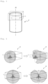
- the radiofrequency system 1 is here integrated into the upper part of an access point 2 having a “tower” structure and which has a generally cylindrical shape with axis A1.
- Access point 2 is for example a Wi-Fi access point.
- the radiofrequency system 1 here comprises an antenna system arranged to operate according to the MIMO technique.
- the radiofrequency system 1 allows to control the shape of the radiation pattern of this MIMO system using a circuit external to the antenna system.
- the control of the shape of the radiation pattern is carried out without intervening on the parameters of the radiofrequency components connected to the antenna system (chips, front-end modules (or FEMs), etc.), nor on the antenna system itself.
- the control carried out does not consist in modifying the number of spatial streams, nor in defining the phase shift between the signals on each antenna, nor in using a precise number of antennas and in choosing which antennas will transmit and receive.
- the radio frequency system 1 allows to create an attenuation or an increase in the gain of a single antenna or of an antenna system in a precise direction, on command, with a reflection system with obstacle by polarization. This control does not act on the operation of the antenna system and does not intervene on the physical layers of the radio interface concerned, which are controlled by a processor and other electronic chips with specific algorithms.
- the radio frequency system 1 comprises a main antenna or a system of main antennas, and a radiation pattern matching device. It can, on command, present either a first radiation pattern, close to that of the antenna or antenna system, or a second radiation pattern, different from the first radiation pattern.
- the modified radiation pattern exhibits reduced or increased gain in at least one predetermined direction.
- first radiation patterns 3a, 3b are quasi-isotropic, while the second radiation patterns 4a, 4b present modified gains in certain directions.
- the radiofrequency system 1 comprises at least one main antenna (here four) and, for each main antenna, a radiation pattern matching device adapted to said main antenna.
- the main antenna 5 is a TRX antenna (transmitting and receiving antenna), of the patch antenna type. It has a flat, rectangular shape with a length L1 and a width l1.
- the central frequency is for example equal to 5800 MHz.
- the radiation pattern matching device 6 comprises a printed circuit 8. Its substrate here is an FR4 substrate.
- the printed circuit board 8 has a generally rectangular shape with cut corners.
- the printed circuit board 8 has a length L2 and a width 12.
- Two radiating strands 10 are printed on a first layer (here on the upper layer) of the printed circuit 8.
- the two radiating strands 10 are each of generally rectangular shape, and extend successively along the length of the printed circuit 8.
- each radiating strand 10 is here equal to ⁇ /4.
- ⁇ /4 is the quarter wavelength of the central frequency of the operating band of the main antenna.
- Each radiating strand 10 is therefore a relatively wide printed track.
- the two radiating strands 10 each extend on either side of a central axis A3 of the printed circuit 8 extending along its width.
- each radiating strand 10 closest to said axis A3 has a generally triangular shape (oriented towards the outside of the strand).
- a track 11 extends from the vertex 12 of said triangle then makes a right angle to extend parallel to said axis A3 in the direction of the edge 14 (length) of the printed circuit 8.
- Ground tracks 15 extend on each side of the track 11.
- the track 11 and its ground tracks 15 form a coplanar waveguide 16.
- the 16 coplanar waveguides are 50 Q tracks.
- the two sets are arranged symmetrically with respect to the axis A3.
- a switching circuit 17 is mounted on the printed circuit 8.
- the switching circuit 17 here is a radio frequency SPST switch (SPST for Single Pole Single Throw , or single-pole single-way switch).
- the SPST switch 17 comprises a first port 20 connected to the left radiating strand 10, a second port 21 connected to the right radiating strand 10, a third port 22 (power supply) and a fourth port 23 (control).
- the first port 20 and the second port 21 can therefore be selectively connected (closed state) or disconnected (open state), on command, via the fourth port 23.
- the SPST switch 17 When the control voltage Vc is equal to 0 V, the SPST switch 17 is in the open state. When the control voltage Vc is equal to 3.3 V, the SPST switch 17 is in the closed state.
- the SPST switch 17 therefore makes it possible to establish or cut an electromagnetic connection between the two radiating strands 10. In the closed state, it thus creates the half-wave dipole antenna 18. In the open state, it leaves the radiating strands 10 as very high frequency monopoles.
- the SPST switch 17 therefore sees an impedance of 50 ⁇ at its input and output.
- the SPST 17 switch that is used is a standard component that has been designed for operation at 50 ⁇ (standard impedance for civil radiofrequency applications).
- the use of a standard component is of course interesting from the point of view of the cost of the component, but also of its availability.
- the SPST 17 switch therefore works optimally: it passes the signal with minimal insertion loss and it blocks the signal with maximum attenuation.
- the SPST switch 17 would not be impedance matched and therefore its performance would be degraded.
- the printed circuit 8 further comprises a reflector 25 printed on the printed circuit 8.
- the reflector 25 comprises a main portion 26 which extends over the entire length of the printed circuit 8 along the edge 14. This main portion 26 itself comprises a central portion which goes up towards the center of the printed circuit 8.
- the central portion of the reflector 25 is located in a central portion of the first layer, in which the guides 16 are also positioned.
- the radiating strands 10 extend on either side of said central portion.
- the reflector 25 further comprises two secondary portions 27 which each extend from a separate end of the main portion 26 while being perpendicular thereto.
- the reflector 25 is therefore a track whose length is equal to that of the printed circuit 8, and which is folded in a certain way on the ends, with a certain angle to increase the level of reflectivity. It should also be noted that the wider this track, the more reflective it is. This design was thought out to satisfy a compromise between dimensions, complexity, volume and performance of the solution.
- the printed circuit 8 further comprises a main ground plane 28 printed on a second layer (here on the lower layer of the printed circuit 8).
- the main ground plane 28 is positioned in a central portion of the second layer, superimposed with the central portion of the first layer.
- the ground tracks 15 of the coplanar waveguides 16, the ground plane 29 of the SPST switch 17, as well as the reflector 25, are connected to the main ground plane 28.
- the second layer of the printed circuit also comprises a track 30 connected to the third port 22 of the SPST switch 17 (power supply) and a track 31 connected to the fourth port 23 of the SPST switch 17. These two tracks 30, 31 each end with a rectangular portion 32, 33, having an edge coincident with the edge 14 of the printed circuit 8.
- a first cable 34 on which a power supply voltage Vcc runs, is soldered to the portion 32.
- a second cable 35 on which a control voltage Vc runs, is soldered to the portion 33.
- the access point 2 comprises a motherboard 40 which comprises radio frequency components.
- the main antenna 5 is connected to the motherboard via a coaxial cable 41 (50 ⁇ ).
- the first cable 34 and the second cable 35 are connected to the motherboard 8.
- the motherboard 40 includes a power supply unit 42 and a processing unit 43.
- the power supply unit 42 supplies the supply voltage Vcc to the SPST switch 17 (via the first cable 34).
- the processing unit 43 supplies the control voltage Vc to the SPST switch 17 (via the second cable 35). It is therefore the processing unit 43 which controls the evolution of the radiation pattern of the radiofrequency system (change from the first radiation pattern to the second radiation pattern, and vice versa).
- the processing unit 43 comprises at least one processing component 43a, which is for example a “generalist” processor, a processor specialized in signal processing (or DSP, for Digital Signal Processor ), a microcontroller, or a programmable logic circuit such as an FPGA (for Field Programmable Gate Arrays ) or an ASIC (for Application Specified Integrated Circuit ) .
- a “generalist” processor for example a “generalist” processor, a processor specialized in signal processing (or DSP, for Digital Signal Processor ), a microcontroller, or a programmable logic circuit such as an FPGA (for Field Programmable Gate Arrays ) or an ASIC (for Application Specified Integrated Circuit ) .
- DSP Digital Signal Processor
- microcontroller for Microcontroller
- a programmable logic circuit such as an FPGA (for Field Programmable Gate Arrays ) or an ASIC (for Application Specified Integrated Circuit ) .
- the processing unit 43 further comprises one or more memories 43b, connected to or integrated in the processing component 43a. At least one of these memories 43b forms a computer-readable recording medium, on which at least one computer program is recorded comprising instructions which drive the processing component. 43a to perform at least some of the steps of the following piloting process.
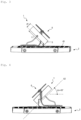
- the main antenna 5 extends in a first plane P1
- the printed circuit 8 extends in a second plane P2 perpendicular to the first plane P1.
- the radiation pattern matching device 6 is therefore positioned perpendicularly above the main antenna 5.
- a first distance d1 between the main antenna 5 and the printed circuit 8, along a first axis X1 passing through the first plane P1 and perpendicular to the second plane P2, is equal to ⁇ /8.
- a second distance d2 between the main antenna 5 and the printed circuit 8, along a second axis X2 contained in the second plane and perpendicular to the second axis, is equal to ⁇ /16.
- the radiation pattern matching device 6 is therefore spaced from the main antenna 5 by ⁇ /8 on the vertical plane and ⁇ /16 on the horizontal plane by a frequency chosen (by calculating the wavelength in free space with ⁇ r and ⁇ r equal to 1).
- the main antenna 5 and the radiation pattern matching device 6 are connected to a common ground.
- This common ground is also a ground of the access point 2. It includes a metal grid 45 belonging to the chassis of the access point 2.
- the radiofrequency system 1 comprises a spring ground contact 46, which is fixed to the ground plane 28 of the printed circuit 8 and to the metal grid 45.
- the radiofrequency system 1 When the SPST switch 17 is in the open state (blocked mode), the flow of current between the two radiating strands 10 is blocked and the radiofrequency system 1 has a first radiation pattern, which is substantially that of the main antenna 5 alone (it is not perfectly identical due to the influence of the printed circuit and the tracks printed on it).
- the dipole antenna 18 formed on the printed circuit board 8 of the pattern matching device radiation 6 partially receives the radiofrequency signal emitted by the main antenna 5.
- the main antenna 5 By emitting an electromagnetic wave, the main antenna 5 generates an electric field E and a magnetic field H in the space around it with a more or less different mapping in accordance with its radiation pattern.
- the electric field induces in this case a voltage in the PR antenna between its radiating strands 10, and the magnetic field induces a surface current on the same radiating conductive parts.
- This voltage and current flowing on the PR antenna then create an electromagnetic field, with a different spatial mapping governed by its radiation pattern.
- the combination of the electromagnetic fields generated by the main antenna and the PR antenna creates a combined radiation pattern with a particular shape oriented mainly in a predetermined direction. This phenomenon is completely passive.
- the design of the PR antenna, equipped with the reflector 25 printed on the printed circuit 8, increases the directivity of the combined radiation, because the received waves are reflected.
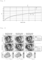
- the magnetic field is maximum in the Z1 zones (greater than 1 A/m).
- the electric field is maximum in the Z2 zones (greater than 300 V/m).
- the gain of the radiation pattern increases towards the negative side of the X axis, and decreases in the other direction. Hole 47 is accentuated.
- the radiofrequency system 1 then has a second radiation pattern having, relative to the first radiation pattern, an increased or decreased gain in at least one predetermined direction.
- the reception efficiency of the PR antenna therefore depends on several factors, such as the distance between the antennas, the position of the two antennas, the relative orientation, the radiation characteristics of the main antenna as well as the dimensions and electrical properties of the PR antenna.
- the PR antenna therefore acts essentially as a passive receiver and reflector that can capture part of the signal emitted and/or received by the main antenna. It does not amplify or improve the quality of the signal.
- the proximity of the main antenna 5 and the radiation pattern matching device 6 modifies the characteristics of the main antenna 5, and this in a different manner if the radiation pattern matching device 6 forms a reflective half-wave dipole antenna (switch: closed state) or if the metal elements formed by the radiating strands are separated (switch: open state).
- the return loss of the main antenna 5 (curve C9) is low (less than -10 dB) over a wider bandwidth than the useful bandwidth 48 (operating frequency band). This makes it possible to anticipate a frequency shift due to its proximity to the PR antenna and to avoid a drop in its efficiency which could deteriorate the performance of its radiation and which could deteriorate the performance of the access point 2 because of the conducted reflection level being too high.
- the return loss of the PR antenna (C10 curve) must also be low (less than -10dB) in the operating frequency band so that it can have the desired impact on the main antenna.
- the transmission coefficient (curve C11) between the two antennas i.e. the coupling, must not be too strong so as not to impact too much the efficiency of the main antenna 5 and must not be too weak to create a real distinction between the two closed/open states of the SPST switch 17.
- the transmission coefficient between the main antenna 5 and the radiation pattern matching device 6 is between -15 dB and -6 dB.
- Table 1 (Appendix 1) illustrates an example of behavior obtained for a radiofrequency system. comprising a main antenna and the radiation pattern matching device.
- the first column corresponds to the first distance between the main antenna and the radiation pattern matching device (along the X1 axis).
- the fourth row corresponds to the optimal position previously described.
- the second column corresponds to the state of the SPST switch.
- the third column gives the directivity values for the three frequencies: 5180 MHz, 5500 MHz and 5800 MHz.
- the fourth column gives the "relative" directivity offsets with respect to the switch state and position.
- the fifth column gives the efficiency and the sixth column the field components (in %).
- Table 2 (Appendix 2) is a similar table to Table 1, except that this time, in the first column, it is the inclination of the radiation pattern matching device 6 that varies.
- the switching circuit i.e. the polarizing element of the receiving/reflecting device, is an SPST switch.
- the switching circuit therefore does not necessarily include an SPST switch.
- the switching circuit can for example be a diode switching circuit.
- the switching circuit 50 comprises a first capacitor 51 having a first terminal connected to the radiating strands 10 and to the reflector 25, a first inductor 52 having a first terminal connected to the second terminal of the first capacitor 51 and a second terminal connected to the electrical ground.
- the cathode of the diode 53 is connected to the second terminal of the first capacitor 51 (and to the first terminal of the first inductor 52).
- the anode of the diode 53 is connected to a first terminal of the second capacitor 54.
- the second terminal of the second capacitor 54 is connected to the common ground of the equipment.
- the circuit further comprises a second inductor 55 connected in series with a resistor 56 and a voltage source 57.
- the second inductor 55 has a first terminal connected to the anode of the diode 53 and a second terminal connected to the resistor 56.
- This circuit has certain disadvantages: relatively high cost, difficulty in finding in stores ultra-low capacitance radio frequency diodes covering a wide frequency band and supporting high input power.
- diode 53 is permanently biased, and therefore either permanently passing or blocking, which cancels the desired function.
- the SPST 17 switch is easily found in the trade. Its characteristics are known and more interesting for the present application.
- This component acts as a switch that can let a radio frequency signal pass with a low insertion loss or block it with an isolation around 30dB on the band 5 to 6GHz. It can support a maximum input power of 30dBm, which is more than enough.
- the main antenna 5 and the radiation pattern matching device 6 are mounted on the same support 60 made of plastic (in one piece).
- the support 60 comprises a first part 61 for accommodating the main antenna and holding it in the position as shown in the Figures 3 to 5 .
- the support 60 comprises a second part 62 for accommodating the radiation pattern adaptation device.
- the second part comprises a flat surface 63, of generally rectangular shape, having substantially the same dimensions as the printed circuit 8.
- the second part 62 also comprises a set of tabs each comprising a first portion which extends perpendicular to the flat surface 63 and from an edge thereof, and a second portion which extends perpendicular to the first portion and towards the inside of the flat surface 63.
- the set of tabs comprises, for the edge 64 (length of the flat surface) of the flat surface, a tab 65 located approximately in the center of said edge and of reduced length, a tab 66 located close to the edge 67 (width of the flat surface 63), also of reduced length.
- the set of tabs also comprises a tab 68 which extends over the entire length of the edge 69 (width of the flat surface) and which extends over a portion of the length of the edge 70 (length of the flat surface) close to half of it.
- a flexible finger 71 comprising a flat running portion, is defined in the thickness of the flat surface 63.
- the finger 71 has an end fixed to the flat surface 63 and a free end from which extends a hook 72 which projects perpendicularly to the flat surface 63 at the edge 67.
- the radiation pattern matching device 6 is manually installed in the holder 60 in the following manner.
- the printed circuit 8 is inserted into the holder 60 by being introduced by the edge 67 of the flat surface 63, and by pressing on the hook 72.
- the printed circuit 8 slides into the space formed between the flat surface 63 and the second portions of the tabs.
- the hook 72 is no longer depressed and projects at the edge 75 of the printed circuit 8 to the outside thereof and by pressing against it, which holds the printed circuit 8 in place.
- the insertion of the printed circuit 8 into the holder is therefore carried out via a sliding connection (produced by means of the tabs), and its retention is carried out via an elastic fitting (produced by the flexible finger 71).
- the radiation pattern matching device 6 can therefore be inserted into its holder and removed manually.
- the access point 2 comprises a plurality of radiofrequency systems 1 as previously described, the main antennas 5 of said radiofrequency systems being arranged to operate according to the MIMO technique.
- the access point has four radio frequency systems 1.
- the support 60 previously mentioned has an octagonal shape. It carries the four main antennas 5 and the four radiation pattern adaptation devices 6.
- the plastic support 60 comprises four large faces 81 and four small faces 82 connecting said large faces 81.
- Each radiofrequency system 1, comprising a main antenna 5 and a radiation pattern matching device 6, is associated with a separate large face 81.
- the support 60 is arranged so that the main antenna 5 extends outside the support 60 while being oriented at 45° and being pressed against the external wall of said large face 81, while the radiation pattern matching device 6 is located inside the support 60 (the edge 64 of the flat surface 63 runs along the internal wall of said large face 81).
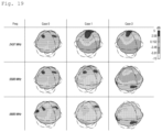
- Table 3 of Appendix 3 lists different cases, each corresponding to a distinct combination of the modes of the radiation pattern matching devices.
- case 0 corresponds to a case where the radiation pattern matching devices are not mounted
- case 1 corresponds to a case where the radiation pattern matching devices are mounted but are all in the off mode
- case 3 corresponds to a case where the matching devices are mounted and are all in the on mode.
- NHPRP Near Field Horizontal Partial Radiated Power
- the characteristics of the reflector are such that the reflector is adapted to control the radiation pattern of the main antenna for different center frequencies respectively associated with different operating bands, such as the operating bands included in the so-called "6 GHz" band of the Wi-Fi 6E protocol.
- the reflector could have a different shape, for an even higher level of reflectivity.
- the corners of the radiation pattern matching device PCB are not necessarily cut out.
- the main antenna is positioned in a vertical plane by being oriented so as to form an angle of 45° with a horizontal plane.
- the radio frequency system can be implemented regardless of the position and orientation of the main antenna.
- the optimized position of the radiation pattern matching device with respect to the main antenna which has been described earlier, is a relative position with respect to the position and orientation of the antenna.
- the main antenna frequency for example, could be different from the frequencies listed here.
- the radio frequency system may include any number of main antennas.
- the shape of the access point could be different.
- it could be a cylindrical shape with a rectangular or square section, possibly with rounded corners.
- the radio frequency system can be integrated into any type of equipment that implements radio frequency communication.
- Table 1 is divided here into two tables: 1A, 1B (which form the same table) table 1A State Total directivity (dB) Total Directivity Offset (dB) Efficiency (dB) 5180 MHz 5500 MHz 5800 MHz 5180 MHz 5500 MHz 5800 MHz 5180 MHz 5500 MHz 5800 MHz Relative switch mode Relative Position Relative switch mode Relative Position Relative switch mode Relative Position +10 mm ON 5 5.6 5.6 -1 1.3 -0.5 0.7 0 0.8 -0.36 -0.26 -0.34 OFF 6 6.1 5.6 -1.4 -0.9 0.2 -0.31 -0.27 -0.43 +5 mm ON 5.5 6 5.5 -0.3 0.8 0 0.3 0.1 0.9 -0.53 -0.35 -0.53 OFF 5.8 6 5.4 -1.2 -0.8 0.4 -0.32 -0.31 -0.53 Initial Position 0 mm ON 6.3 6.3 6.4 17 1.1 0.6 -1.
Landscapes
- Engineering & Computer Science (AREA)
- Computer Networks & Wireless Communication (AREA)
- Variable-Direction Aerials And Aerial Arrays (AREA)
- Aerials With Secondary Devices (AREA)
Applications Claiming Priority (1)
| Application Number | Priority Date | Filing Date | Title |
|---|---|---|---|
| FR2306917A FR3150652B1 (fr) | 2023-06-29 | 2023-06-29 | Diagramme de rayonnement adaptable par polarisation d’obstacle |
Publications (2)
| Publication Number | Publication Date |
|---|---|
| EP4485687A1 true EP4485687A1 (de) | 2025-01-01 |
| EP4485687B1 EP4485687B1 (de) | 2026-04-08 |
Family
ID=88291182
Family Applications (1)
| Application Number | Title | Priority Date | Filing Date |
|---|---|---|---|
| EP24184094.1A Active EP4485687B1 (de) | 2023-06-29 | 2024-06-24 | Durch hindernisvorspannung anpassbares strahlungsdiagramm |
Country Status (4)
| Country | Link |
|---|---|
| US (1) | US20250007172A1 (de) |
| EP (1) | EP4485687B1 (de) |
| CA (1) | CA3244314A1 (de) |
| FR (1) | FR3150652B1 (de) |
Citations (3)
| Publication number | Priority date | Publication date | Assignee | Title |
|---|---|---|---|---|
| US20060044205A1 (en) * | 2004-08-13 | 2006-03-02 | Interdigital Technology Corporation | Compact smart antenna for wireless applications and associated methods |
| US20070152893A1 (en) * | 2002-02-01 | 2007-07-05 | Ipr Licensing, Inc. | Aperiodic array antenna |
| US20090046019A1 (en) * | 2004-10-01 | 2009-02-19 | Matsushita Electric Industrial Co., Ltd. | Antenna device and wireless terminal using the antenna device |
Family Cites Families (2)
| Publication number | Priority date | Publication date | Assignee | Title |
|---|---|---|---|---|
| US6762722B2 (en) * | 2001-05-18 | 2004-07-13 | Ipr Licensing, Inc. | Directional antenna |
| JP2008109214A (ja) * | 2006-10-23 | 2008-05-08 | Matsushita Electric Ind Co Ltd | アンテナ装置 |
-
2023
- 2023-06-29 FR FR2306917A patent/FR3150652B1/fr active Active
-
2024
- 2024-06-24 EP EP24184094.1A patent/EP4485687B1/de active Active
- 2024-06-25 CA CA3244314A patent/CA3244314A1/fr active Pending
- 2024-06-28 US US18/758,913 patent/US20250007172A1/en active Pending
Patent Citations (3)
| Publication number | Priority date | Publication date | Assignee | Title |
|---|---|---|---|---|
| US20070152893A1 (en) * | 2002-02-01 | 2007-07-05 | Ipr Licensing, Inc. | Aperiodic array antenna |
| US20060044205A1 (en) * | 2004-08-13 | 2006-03-02 | Interdigital Technology Corporation | Compact smart antenna for wireless applications and associated methods |
| US20090046019A1 (en) * | 2004-10-01 | 2009-02-19 | Matsushita Electric Industrial Co., Ltd. | Antenna device and wireless terminal using the antenna device |
Also Published As
| Publication number | Publication date |
|---|---|
| EP4485687B1 (de) | 2026-04-08 |
| CA3244314A1 (fr) | 2026-01-19 |
| FR3150652A1 (fr) | 2025-01-03 |
| US20250007172A1 (en) | 2025-01-02 |
| FR3150652B1 (fr) | 2025-10-17 |
Similar Documents
| Publication | Publication Date | Title |
|---|---|---|
| EP0457880B1 (de) | Iff-bordantenne mit schaltbaren strahlungsdiagrammen | |
| EP3843202A1 (de) | Horn für eine zirkular polarisierte duale ka-band-satellitenantenne | |
| EP2710676B1 (de) | Strahlerelement für eine aktive gruppenantenne aus elementarfliesen | |
| WO2008065311A2 (fr) | Antenne multi secteurs | |
| FR2817661A1 (fr) | Dispositif pour la reception et/ou l'emission de signaux multifaisceaux | |
| EP1690317B1 (de) | Doppeltpolarisierte mehrband-gruppenantenne | |
| EP1466384B1 (de) | Einrichtung zum empfangen und/oder emittieren elektromagnetischer wellen mit strahlungs-diversity | |
| EP1516393B1 (de) | Doppelpolarisations-doppelbandstrahlungseinrichtung | |
| EP1346442A1 (de) | Gedruckte patch-antenne | |
| EP4485687B1 (de) | Durch hindernisvorspannung anpassbares strahlungsdiagramm | |
| EP4167378B1 (de) | Isolierte hochfrequenzantennenanordnung | |
| CA2808511C (fr) | Antenne plane pour terminal fonctionnant en double polarisation circulaire, terminal aeroporte et systeme de telecommunication par satellite comportant au moins une telle antenne | |
| EP0991135A1 (de) | Selektive Antenne mit Frequenzumschaltung | |
| FR2930844A1 (fr) | Antenne rf d'emission et/ou de reception comportant des elements rayonnants excites par couplage electromagnetique sans contact | |
| EP2889955B1 (de) | Kompaktantennenstruktur für Telekommunikationen über Satelliten | |
| EP3902059A1 (de) | Breitband-richtantenne mit longitudinalwellen-übertragung | |
| WO2021074505A1 (fr) | Antenne-reseau | |
| WO2025032295A1 (fr) | Système antennaire et antenne réseau correspondante | |
| FR2981514A1 (fr) | Systeme antennaire a une ou plusieurs spirale(s) et reconfigurable | |
| WO2025037062A1 (fr) | Système de réseau d'antennes multi-bandes et superdirectif | |
| Mahmood | Antennes Reconfigurables en Diagramme de Rayonnement à Base de Surfaces Sélectives de Fréquence | |
| EP2096708A1 (de) | Kraftfahrzeugantenne, insbesondere für den Empfang von terrestrischen und/oder Satelliten-Funksignalen | |
| FR2753568A1 (fr) | Antenne-reseau polyvalente | |
| Mahmood | Antennes reconfigurables en diagramme de rayonnement à base de surfaces sélectives de fréquence/Reconfigurable Radiation Pattern Antennas Based on Frequency Selective Surfaces. | |
| EP1873864A1 (de) | Symmetrische Antenne für Mikrostreifenleitertechnologie |
Legal Events
| Date | Code | Title | Description |
|---|---|---|---|
| PUAI | Public reference made under article 153(3) epc to a published international application that has entered the european phase |
Free format text: ORIGINAL CODE: 0009012 |
|
| STAA | Information on the status of an ep patent application or granted ep patent |
Free format text: STATUS: REQUEST FOR EXAMINATION WAS MADE |
|
| STAA | Information on the status of an ep patent application or granted ep patent |
Free format text: STATUS: EXAMINATION IS IN PROGRESS |
|
| 17P | Request for examination filed |
Effective date: 20240624 |
|
| AK | Designated contracting states |
Kind code of ref document: A1 Designated state(s): AL AT BE BG CH CY CZ DE DK EE ES FI FR GB GR HR HU IE IS IT LI LT LU LV MC ME MK MT NL NO PL PT RO RS SE SI SK SM TR |
|
| 17Q | First examination report despatched |
Effective date: 20241213 |
|
| GRAP | Despatch of communication of intention to grant a patent |
Free format text: ORIGINAL CODE: EPIDOSNIGR1 |
|
| STAA | Information on the status of an ep patent application or granted ep patent |
Free format text: STATUS: GRANT OF PATENT IS INTENDED |
|
| INTG | Intention to grant announced |
Effective date: 20251112 |
|
| GRAS | Grant fee paid |
Free format text: ORIGINAL CODE: EPIDOSNIGR3 |
|
| GRAA | (expected) grant |
Free format text: ORIGINAL CODE: 0009210 |
|
| STAA | Information on the status of an ep patent application or granted ep patent |
Free format text: STATUS: THE PATENT HAS BEEN GRANTED |
|
| AK | Designated contracting states |
Kind code of ref document: B1 Designated state(s): AL AT BE BG CH CY CZ DE DK EE ES FI FR GB GR HR HU IE IS IT LI LT LU LV MC ME MK MT NL NO PL PT RO RS SE SI SK SM TR |
|
| REG | Reference to a national code |
Ref country code: CH Ref legal event code: F10 Free format text: ST27 STATUS EVENT CODE: U-0-0-F10-F00 (AS PROVIDED BY THE NATIONAL OFFICE) Effective date: 20260408 Ref country code: GB Ref legal event code: FG4D Free format text: NOT ENGLISH |
|
| REG | Reference to a national code |
Ref country code: DE Ref legal event code: R096 Ref document number: 602024003771 Country of ref document: DE |