EP4485957A2 - Module de caméra et dispositif optique le comprenant - Google Patents
Module de caméra et dispositif optique le comprenant Download PDFInfo
- Publication number
- EP4485957A2 EP4485957A2 EP24213360.1A EP24213360A EP4485957A2 EP 4485957 A2 EP4485957 A2 EP 4485957A2 EP 24213360 A EP24213360 A EP 24213360A EP 4485957 A2 EP4485957 A2 EP 4485957A2
- Authority
- EP
- European Patent Office
- Prior art keywords
- circuit board
- printed circuit
- stiffener
- image sensor
- disposed
- Prior art date
- Legal status (The legal status is an assumption and is not a legal conclusion. Google has not performed a legal analysis and makes no representation as to the accuracy of the status listed.)
- Pending
Links
Images








Classifications
-
- H—ELECTRICITY
- H04—ELECTRIC COMMUNICATION TECHNIQUE
- H04N—PICTORIAL COMMUNICATION, e.g. TELEVISION
- H04N23/00—Cameras or camera modules comprising electronic image sensors; Control thereof
- H04N23/50—Constructional details
- H04N23/52—Elements optimising image sensor operation, e.g. for electromagnetic interference [EMI] protection or temperature control by heat transfer or cooling elements
-
- G—PHYSICS
- G03—PHOTOGRAPHY; CINEMATOGRAPHY; ANALOGOUS TECHNIQUES USING WAVES OTHER THAN OPTICAL WAVES; ELECTROGRAPHY; HOLOGRAPHY
- G03B—APPARATUS OR ARRANGEMENTS FOR TAKING PHOTOGRAPHS OR FOR PROJECTING OR VIEWING THEM; APPARATUS OR ARRANGEMENTS EMPLOYING ANALOGOUS TECHNIQUES USING WAVES OTHER THAN OPTICAL WAVES; ACCESSORIES THEREFOR
- G03B17/00—Details of cameras or camera bodies; Accessories therefor
- G03B17/02—Bodies
-
- G—PHYSICS
- G02—OPTICS
- G02B—OPTICAL ELEMENTS, SYSTEMS OR APPARATUS
- G02B27/00—Optical systems or apparatus not provided for by any of the groups G02B1/00 - G02B26/00, G02B30/00
- G02B27/64—Imaging systems using optical elements for stabilisation of the lateral and angular position of the image
- G02B27/646—Imaging systems using optical elements for stabilisation of the lateral and angular position of the image compensating for small deviations, e.g. due to vibration or shake
-
- G—PHYSICS
- G02—OPTICS
- G02B—OPTICAL ELEMENTS, SYSTEMS OR APPARATUS
- G02B7/00—Mountings, adjusting means, or light-tight connections, for optical elements
- G02B7/02—Mountings, adjusting means, or light-tight connections, for optical elements for lenses
- G02B7/04—Mountings, adjusting means, or light-tight connections, for optical elements for lenses with mechanism for focusing or varying magnification
- G02B7/09—Mountings, adjusting means, or light-tight connections, for optical elements for lenses with mechanism for focusing or varying magnification adapted for automatic focusing or varying magnification
-
- G—PHYSICS
- G03—PHOTOGRAPHY; CINEMATOGRAPHY; ANALOGOUS TECHNIQUES USING WAVES OTHER THAN OPTICAL WAVES; ELECTROGRAPHY; HOLOGRAPHY
- G03B—APPARATUS OR ARRANGEMENTS FOR TAKING PHOTOGRAPHS OR FOR PROJECTING OR VIEWING THEM; APPARATUS OR ARRANGEMENTS EMPLOYING ANALOGOUS TECHNIQUES USING WAVES OTHER THAN OPTICAL WAVES; ACCESSORIES THEREFOR
- G03B13/00—Viewfinders; Focusing aids for cameras; Means for focusing for cameras; Autofocus systems for cameras
- G03B13/32—Means for focusing
- G03B13/34—Power focusing
- G03B13/36—Autofocus systems
-
- G—PHYSICS
- G03—PHOTOGRAPHY; CINEMATOGRAPHY; ANALOGOUS TECHNIQUES USING WAVES OTHER THAN OPTICAL WAVES; ELECTROGRAPHY; HOLOGRAPHY
- G03B—APPARATUS OR ARRANGEMENTS FOR TAKING PHOTOGRAPHS OR FOR PROJECTING OR VIEWING THEM; APPARATUS OR ARRANGEMENTS EMPLOYING ANALOGOUS TECHNIQUES USING WAVES OTHER THAN OPTICAL WAVES; ACCESSORIES THEREFOR
- G03B17/00—Details of cameras or camera bodies; Accessories therefor
- G03B17/02—Bodies
- G03B17/12—Bodies with means for supporting objectives, supplementary lenses, filters, masks, or turrets
-
- G—PHYSICS
- G03—PHOTOGRAPHY; CINEMATOGRAPHY; ANALOGOUS TECHNIQUES USING WAVES OTHER THAN OPTICAL WAVES; ELECTROGRAPHY; HOLOGRAPHY
- G03B—APPARATUS OR ARRANGEMENTS FOR TAKING PHOTOGRAPHS OR FOR PROJECTING OR VIEWING THEM; APPARATUS OR ARRANGEMENTS EMPLOYING ANALOGOUS TECHNIQUES USING WAVES OTHER THAN OPTICAL WAVES; ACCESSORIES THEREFOR
- G03B30/00—Camera modules comprising integrated lens units and imaging units, specially adapted for being embedded in other devices, e.g. mobile phones or vehicles
-
- G—PHYSICS
- G03—PHOTOGRAPHY; CINEMATOGRAPHY; ANALOGOUS TECHNIQUES USING WAVES OTHER THAN OPTICAL WAVES; ELECTROGRAPHY; HOLOGRAPHY
- G03B—APPARATUS OR ARRANGEMENTS FOR TAKING PHOTOGRAPHS OR FOR PROJECTING OR VIEWING THEM; APPARATUS OR ARRANGEMENTS EMPLOYING ANALOGOUS TECHNIQUES USING WAVES OTHER THAN OPTICAL WAVES; ACCESSORIES THEREFOR
- G03B5/00—Adjustment of optical system relative to image or object surface other than for focusing
-
- H—ELECTRICITY
- H04—ELECTRIC COMMUNICATION TECHNIQUE
- H04N—PICTORIAL COMMUNICATION, e.g. TELEVISION
- H04N23/00—Cameras or camera modules comprising electronic image sensors; Control thereof
- H04N23/50—Constructional details
- H04N23/54—Mounting of pick-up tubes, electronic image sensors, deviation or focusing coils
-
- H—ELECTRICITY
- H04—ELECTRIC COMMUNICATION TECHNIQUE
- H04N—PICTORIAL COMMUNICATION, e.g. TELEVISION
- H04N23/00—Cameras or camera modules comprising electronic image sensors; Control thereof
- H04N23/57—Mechanical or electrical details of cameras or camera modules specially adapted for being embedded in other devices
-
- H—ELECTRICITY
- H04—ELECTRIC COMMUNICATION TECHNIQUE
- H04N—PICTORIAL COMMUNICATION, e.g. TELEVISION
- H04N23/00—Cameras or camera modules comprising electronic image sensors; Control thereof
- H04N23/60—Control of cameras or camera modules
- H04N23/68—Control of cameras or camera modules for stable pick-up of the scene, e.g. compensating for camera body vibrations
- H04N23/682—Vibration or motion blur correction
- H04N23/685—Vibration or motion blur correction performed by mechanical compensation
-
- H—ELECTRICITY
- H04—ELECTRIC COMMUNICATION TECHNIQUE
- H04N—PICTORIAL COMMUNICATION, e.g. TELEVISION
- H04N23/00—Cameras or camera modules comprising electronic image sensors; Control thereof
- H04N23/60—Control of cameras or camera modules
- H04N23/68—Control of cameras or camera modules for stable pick-up of the scene, e.g. compensating for camera body vibrations
- H04N23/682—Vibration or motion blur correction
- H04N23/685—Vibration or motion blur correction performed by mechanical compensation
- H04N23/687—Vibration or motion blur correction performed by mechanical compensation by shifting the lens or sensor position
-
- G—PHYSICS
- G03—PHOTOGRAPHY; CINEMATOGRAPHY; ANALOGOUS TECHNIQUES USING WAVES OTHER THAN OPTICAL WAVES; ELECTROGRAPHY; HOLOGRAPHY
- G03B—APPARATUS OR ARRANGEMENTS FOR TAKING PHOTOGRAPHS OR FOR PROJECTING OR VIEWING THEM; APPARATUS OR ARRANGEMENTS EMPLOYING ANALOGOUS TECHNIQUES USING WAVES OTHER THAN OPTICAL WAVES; ACCESSORIES THEREFOR
- G03B2205/00—Adjustment of optical system relative to image or object surface other than for focusing
- G03B2205/0007—Movement of one or more optical elements for control of motion blur
-
- G—PHYSICS
- G03—PHOTOGRAPHY; CINEMATOGRAPHY; ANALOGOUS TECHNIQUES USING WAVES OTHER THAN OPTICAL WAVES; ELECTROGRAPHY; HOLOGRAPHY
- G03B—APPARATUS OR ARRANGEMENTS FOR TAKING PHOTOGRAPHS OR FOR PROJECTING OR VIEWING THEM; APPARATUS OR ARRANGEMENTS EMPLOYING ANALOGOUS TECHNIQUES USING WAVES OTHER THAN OPTICAL WAVES; ACCESSORIES THEREFOR
- G03B2217/00—Details of cameras or camera bodies; Accessories therefor
- G03B2217/002—Details of arrangement of components in or on camera body
-
- H—ELECTRICITY
- H04—ELECTRIC COMMUNICATION TECHNIQUE
- H04N—PICTORIAL COMMUNICATION, e.g. TELEVISION
- H04N23/00—Cameras or camera modules comprising electronic image sensors; Control thereof
- H04N23/50—Constructional details
- H04N23/55—Optical parts specially adapted for electronic image sensors; Mounting thereof
Definitions
- Embodiments relate to a camera module and an optical device including the same.
- VCM voice coil motor
- the camera module may frequently receive shocks when in use, and may undergo fine shaking due to, for example, user hand tremor while capturing an image.
- technology for additionally installing a device for inhibiting transfer of hand tremor to a camera module has recently been developed.
- Embodiments provide a camera module and an optical device capable of improving optical performance, securing reliability of wire bonding between a printed circuit board and an image sensor, and increasing bonding force between a stiffener and the image sensor.
- a camera module may include a lens barrel, a holder, a filter disposed in the holder, a printed circuit board having therein an opening, a stiffener including a first region corresponding to the opening and a second region in which the printed circuit board is disposed, and an image sensor disposed in the first region of the stiffener.
- the first region of the stiffener may include a protruding portion protruding further than the second region of the stiffener, and the image sensor may be disposed on the upper surface of the protruding portion.
- the height from the lower surface of the stiffener to the upper surface of the protruding portion may be less than the height to the upper surface of the printed circuit board disposed on the stiffener.
- the protruding portion may include a plurality of protrusions spaced apart from each other.
- the camera module may further include an adhesive member disposed in the space between the upper surfaces of the plurality of protrusions and the lower surface of the image sensor and in the space between the plurality of protrusions.
- the thickness of the image sensor may be less than the thickness of the printed circuit board.
- the camera module may further include a first adhesive member disposed between the second region of the stiffener and the lower surface of the printed circuit board.
- the first adhesive member may include therein an opening corresponding to the opening in the printed circuit board.
- the camera module may further include a second adhesive member disposed between the upper surface of the protruding portion and the lower surface of the image sensor.
- the second adhesive member may be located at a higher position than the first adhesive member.
- the printed circuit board may include a first terminal, and the image sensor may include a second terminal.
- the camera module may further include a wire connecting the first terminal to the second terminal.
- the ratio of the first height from the upper surface of the second region of the stiffener to the upper surface of the protruding portion to the second height from the lower surface of the stiffener to the upper surface of the second region of the stiffener may be 1:0.67 to 1:2.1.
- a camera module may include a lens barrel, a holder, a filter disposed in the holder, a printed circuit board having therein an opening, a stiffener including a first region corresponding to the opening and a second region in which the printed circuit board is disposed, and an image sensor disposed in the first region of the stiffener.
- the first region of the stiffener may include a cavity recessed further than the second region of the stiffener, and the image sensor may be disposed on the bottom surface of the cavity.
- a camera module may include a lens barrel, a holder, a filter disposed in the holder, a printed circuit board having therein an opening, a stiffener including a first region corresponding to the opening and a second region in which the printed circuit board is disposed, an image sensor disposed in the first region of the stiffener, and an adhesive member including a first adhesive member disposed between the first region of the stiffener and the image sensor and a second adhesive member disposed between the second region of the stiffener and the printed circuit board.
- the first adhesive member and the second adhesive member may be connected to each other.
- Embodiments are capable of improving the optical performance of a camera module, securing reliability of wire bonding between a printed circuit board and an image sensor, and increasing bonding force between a stiffener and the image sensor.
- a camera module and an optical device including the same according to embodiments will be described with reference to the accompanying drawings.
- a camera module according to the embodiments will be described using the Cartesian coordinate system (x, y, z), but the embodiments are not limited thereto, and may be described using other coordinate systems.
- the x-axis and the y-axis may be directions perpendicular to the z-axis, which is an optical-axis (OA) direction
- the z-axis direction which is the optical-axis (OA) direction
- the x-axis direction may be referred to as a 'second direction'
- the y-axis direction may be referred to as a ⁇ third direction'.
- a 'hand tremor compensation function' applied to a small camera module of a mobile device such as a smartphone or a tablet PC may be a function of moving a lens in a direction perpendicular to the optical-axis direction or tilting the lens with respect to the optical axis so as to cancel vibration (or motion) caused by user hand tremor.
- an ⁇ autofocus function' may be a function of automatically focusing on an object by moving the lens in the optical-axis direction according to the distance to the object so that an image sensor obtains a clear image of the object.
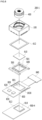
- FIG. 1 is an exploded perspective view of a camera module 200 according to an embodiment
- FIG. 2 is a cross-sectional view of an embodiment of the camera module 200 of FIG. 1
- FIG. 3 is an enlarged view of the portion indicated by the dotted line 15 in FIG. 2 .
- the camera module 200 may include a lens or a lens barrel 400, a lens-moving apparatus 100, a filter 610, a holder 600, a printed circuit board 800, a stiffener 900, and an image sensor 810.
- the "camera module” may be referred to as an "image capture device” or a “photographing device”
- the holder 600 may be referred to as a sensor base.
- the camera module 300 may further include a blocking member 1500 disposed on the filter 610.
- the camera module 300 may further include an adhesive member 612.
- the camera module 300 may further include a motion sensor 820, a controller 830, and a connector 840.
- the lens or the lens barrel 400 may be mounted in a bobbin 110 of the lens-moving apparatus 100.
- the lens-moving apparatus 100 may move the lens or the lens barrel 400.
- the camera module 200 may be any one of an autofocus (AF) camera module and an optical image stabilizer (OIS) camera module.
- the AF camera module is a camera module configured to perform only an autofocus function
- the OIS camera module is a camera module configured to perform an autofocus function and an optical image stabilizer (OIS) function.
- the lens-moving apparatus 100 may be an AF lens-moving apparatus or an OIS lens-moving apparatus, and the meanings of "AF” and "OIS” may be the same as those of the AF camera module and the OIS camera module.
- the lens-moving apparatus 100 of the camera module 200 may be an OIS lens-moving apparatus.
- the lens-moving apparatus 100 may include a housing 140, a bobbin 110 disposed in the housing 140 to allow the lens or the lens barrel 400 to be mounted thereto, a first coil 120 disposed at the bobbin 110, a magnet 130 disposed in the housing 140 so as to face the first coil 120, at least one upper elastic member (not shown) coupled to the upper portion of the bobbin 110 and the upper portion of the housing 140, at least one lower elastic member (not shown) coupled to the lower portion of the bobbin 110 and the lower portion of the housing 140, a second coil 230 disposed under the bobbin 110 (and/or the housing 140), a printed circuit board 250 disposed under the second coil 230, and a base 210 disposed under the printed circuit board 250.
- the lens-moving apparatus 100 may further include a cover member 300 coupled to the base 210 to provide space for accommodating the components of the lens-moving apparatus 100 together with the base 210.
- the lens-moving apparatus 100 may further include a support member (not shown) electrically connecting the printed circuit board 250 to the upper elastic member and supporting the housing 140 with respect to the base 210.
- a support member (not shown) electrically connecting the printed circuit board 250 to the upper elastic member and supporting the housing 140 with respect to the base 210.
- Each of the first coil 120 and the second coil 230 may be electrically connected to the printed circuit board 250, and may receive a driving signal (driving current) from the printed circuit board 250.
- the upper elastic member may include a plurality of upper springs
- the support member may include support members connected to the upper springs
- the first coil 120 may be electrically connected to the printed circuit board 250 via the upper springs and the support member.
- the printed circuit board 250 may include a plurality of terminals, and some of the plurality of terminals may be electrically connected to the first coil 120 and/or the second coil 230.
- the bobbin 110 and the lens or the lens barrel 400 coupled thereto may be moved in the optical-axis direction due to the electromagnetic force generated by interaction between the first coil 120 and the magnet 130, and accordingly, the displacement of the bobbin 110 in the optical-axis direction may be controlled, whereby an AF operation may be implemented.
- the housing 140 may be moved in a direction perpendicular to the optical axis due to the electromagnetic force generated by interaction between the second coil 230 and the magnet 130, and accordingly, a hand tremor compensation or OIS operation may be implemented.
- the lens-moving apparatus 100 of the camera module 200 may further include a sensing magnet (not shown) disposed at the bobbin 110 and an AF position sensor (e.g. a hall sensor) (not shown) disposed in the housing 140.
- the lens-moving apparatus 100 may further include a printed circuit board (not shown) disposed in the housing and/or on the base to allow the AF position sensor to be disposed or mounted thereon.
- the AF position sensor may be disposed at the bobbin, and the sensing magnet may be disposed in the housing.
- the lens-moving apparatus 100 may further include a balancing magnet disposed at the bobbin 110 so as to correspond to the sensing magnet.
- the AF position sensor may output an output signal according to the result of detection of the magnitude of the magnetic field of the sensing magnet upon movement of the bobbin 100.
- the AF position sensor may be electrically connected to the printed circuit board 250 via the upper elastic member (or the lower elastic member) and/or the support member.
- the printed circuit board 250 may provide a driving signal to the AF position sensor, and the output of the AF position sensor may be transmitted to the printed circuit board 250.
- the lens-moving apparatus 100 may be an AF lens-moving apparatus, and the AF lens-moving apparatus may include a housing, a bobbin disposed in the housing, a coil disposed at the bobbin, a magnet disposed in the housing, at least one elastic member coupled to the bobbin and the housing, and a base disposed under the bobbin (and/or the housing).
- the elastic member may include the upper elastic member and the lower elastic member described above.
- a driving signal (e.g. driving current) may be provided to the coil, and the bobbin may be moved in the optical-axis direction due to the electromagnetic force generated by interaction between the coil and the magnet.
- the coil may be disposed in the housing, and the magnet may be disposed at the bobbin.
- the AF lens-moving apparatus may further include a sensing magnet disposed at the bobbin, an AF position sensor (e.g. a hall sensor) disposed in the housing, and a printed circuit board disposed or mounted in the housing and/or on the base to allow the AF position sensor to be mounted thereon.
- the AF position sensor may be disposed at the bobbin, and the sensing magnet may be disposed in the housing.
- the camera module according to another embodiment may include, instead of the lens-moving apparatus 100 of FIG. 1 , a housing coupled to the lens or the lens barrel 400 to fix the lens or the lens barrel 400, and the housing may be coupled or attached to the upper surface of the holder 600.
- the housing attached or fixed to the holder 600 may not be moved, and the position of the housing may be fixed in the state in which the housing is attached to the holder 600.
- the printed circuit board may be electrically connected to the coil and the AF position sensor, a driving signal may be provided to each of the coil and the AF position sensor through the printed circuit board, and the output of the AF position sensor may be transmitted to the printed circuit board.
- the holder 600 may be disposed under the base 210 of the lens-moving apparatus 100.
- the filter 610 may be mounted to the holder 600, and the holder 600 may include a seating portion 500 on which the filter 610 is seated.
- the adhesive member 612 may couple or attach the base 210 of the lens-moving apparatus 100 to the holder 600.
- the adhesive member 612 may be disposed between the lower surface of the base 210 and the upper surface of the holder 600, and may bond these two components to each other.
- the adhesive member 612 may serve not only to bond components, as described above, but also to prevent foreign substances from entering the lens-moving apparatus 100.
- the adhesive member 612 may be an epoxy, a thermosetting adhesive, or an ultraviolet curable adhesive.
- the filter 610 may be disposed in the seating portion 500 of the holder 600.
- the seating portion 500 of the holder 600 may include a protruding portion 500a protruding from the upper surface of the holder 600, without being limited thereto.
- the seating portion may be a recess, a cavity, or a hole, which is concavely formed in the upper surface of the holder 600.
- the protruding portion 500a of the seating portion 500 may serve to prevent the lower end of the lens or the lens barrel 400 from coming into contact with or colliding with the filter 610 (and/or the blocking member 1500).
- the protruding portion 500a may be formed to protrude along the side surface of the filter 610 in the optical-axis direction.
- the protruding portion 500a may be disposed around the side surface of the filter 610 so as to surround the side surface of the filter 610.
- the inner surface of the protruding portion 500a may be provided so as to face the side surface of the filter 610, and these two components may be spaced apart from each other. The reason for this is to secure processing tolerance to facilitate mounting of the filter 610 in the seating portion 500 of the holder 600.
- the upper surface of the protruding portion 500a may be positioned above the upper surface 610 of the filter 610 in the optical-axis direction. The reason for this is to prevent the lower end of the lens or the lens barrel 400 from directly colliding with the filter 610 when the lens or the lens barrel 400 is mounted in the lens-moving apparatus 100 and moves in the optical-axis direction or moves toward the filter 610 due to an external impact.
- the shape of the protruding portion 500a viewed from above may match the shape of the filter 610, without being limited thereto. In another embodiment, the shape of the protruding portion 500a may be similar to or different from the shape of the filter 610.
- the holder 600 may have an opening 501 formed in the region thereof in which the filter 610 is mounted or disposed so that light passing through the filter 610 enters the image sensor 810.
- the opening 501 may penetrate the holder 600 in the optical-axis direction, and may be referred to as a "through-hole".
- the opening 501 may penetrate the center of the holder 600 and may be provided in the seating portion 500, and the area of the opening 501 may be smaller than the area of the filter 610.
- the holder 600 may be disposed on the printed circuit board 800, and may accommodate the filter 610 therein.
- the holder 600 may support the lens-moving apparatus 100 positioned thereon.
- the lower surface of the base 210 of the lens-moving apparatus 100 may be disposed on the upper surface of the holder 600.
- the lower surface of the base 210 of the lens-moving apparatus 100 may be in contact with the upper surface of the holder 600, and may be supported by the upper surface of the holder 600.
- the filter 610 may be disposed in the seating portion 500 of the holder 600.
- the filter 610 may serve to block light in a specific frequency band, among the light passing through the lens barrel 400, from entering the image sensor 810.
- the filter 610 may be an infrared cutoff filter, without being limited thereto.
- the filter 610 may be disposed parallel to the x-y plane, which is perpendicular to the optical axis OA.
- the filter 610 may be attached to the seating portion 500 of the holder 600 using an adhesive member (not shown) such as UV epoxy.
- the printed circuit board 800 may be disposed under the holder 600, and the holder 600 may be disposed on the upper surface of the printed circuit board 800.
- the holder 600 may be attached or fixed to the upper surface of the printed circuit board 800 using an adhesive member such as an epoxy, a thermosetting adhesive, or an ultraviolet curable adhesive.
- the adhesive member may be disposed between the lower surface of the holder 600 and the upper surface of the printed circuit board 800.
- the printed circuit board 800 may have therein an opening 801 corresponding to the opening 501 in the holder 600.
- the opening 801 in the printed circuit board 800 may be a through-hole penetrating the printed circuit board 800 in the optical-axis direction.
- the image sensor 810 may be disposed in the opening 801 in the printed circuit board 800.
- the stiffener 900 may be disposed under the printed circuit board 800, and may include a protruding portion 901 formed corresponding to the opening 801 in the printed circuit board 800 to allow the image sensor 810 to be mounted thereto.
- the protruding portion 901 may protrude from the region of the upper surface of the stiffener 900 in the optical-axis direction.
- the image sensor 810 may be disposed on the upper surface of the protruding portion 901, and may be exposed through the opening 801 in the printed circuit board 800.
- the image sensor 810 disposed on the upper surface of the protruding portion 901 of the stiffener 900 may be electrically connected to the printed circuit board 800 via a wire 21.
- the wire 21 may connect a terminal 813 of the image sensor 810 and a terminal 1830 of the printed circuit board 800 to each other.
- the stiffener 900 is a plate-type member having a predetermined thickness and hardness, and may stably support the image sensor 810 and prevent damage to the image sensor due to an external impact or contact.
- stiffener 900 may improve a heat dissipation effect of dissipating the heat generated from the image sensor to the outside.
- the stiffener 900 may be formed of a metal material having high thermal conductivity, such as SUS or aluminum, without being limited thereto.
- the stiffener 900 may be formed of glass epoxy, plastic, or synthetic resin.
- stiffener 900 may be electrically connected to a ground terminal of the printed circuit board 800, and thus may serve as a ground for protecting the camera module from electrostatic discharge (ESD).
- ESD electrostatic discharge
- the image sensor 810 may be a part on which the light that has passed through the filter 610 is incident and in which an image included in the light is formed.
- the printed circuit board 800 may be provided with various circuits, elements, and controllers in order to convert an image formed by the image sensor 810 into an electrical signal and to transmit the electrical signal to an external device.
- a circuit pattern which is electrically connected to the image sensor and various elements, may be formed on the printed circuit board 800.
- the holder 600 may be referred to as a first holder, and the printed circuit board 800 may be referred to as a second holder.
- the image sensor 810 may receive an image included in the light introduced through the lens-moving apparatus 100, and may convert the received image into an electrical signal.
- the filter 610 and the image sensor 810 may be disposed so as to be spaced apart from each other and to face each other in the optical-axis (OA) direction or the first direction.
- the protruding portion 500a of the holder 600 may be disposed so as to face the filter 610 in the optical-axis direction.
- the blocking member 1500 may be disposed on the upper surface of the filter 610.
- the blocking member 1500 may be referred to as a "masking part".
- the blocking member 1500 may be disposed on the edge portion of the upper surface of the filter 610, and may serve to block at least a portion of the light traveling toward the edge portion of the filter 610 through the lens or the lens barrel 400 from passing through the filter 610.
- the blocking member 1500 may be coupled or attached to the upper surface of the filter 1610.
- the filter 610 may be formed in a rectangular shape when viewed in the optical-axis direction, and the blocking member 1500 may be formed to be symmetrical with respect to the filter 610 along each side of the upper surface of the filter 610.
- the blocking member 1500 may be formed to have a predetermined width on each side of the upper surface of the filter 1610.
- the blocking member 1500 may be formed of an opaque material.
- the blocking member 1500 may be an opaque and adhesive material that is applied to the filter 610, or may be provided in the form of a film that is attached to the filter 610.
- the filter 610 and the image sensor 810 may be disposed so as to face each other in the optical-axis direction, and at least a portion of the blocking member 1500 may overlap the terminal 1830 and/or the wire 21 disposed on the printed circuit board 800 in the optical-axis direction.
- the wire 21 and the terminal 1830 may be formed of a conductive material such as gold, silver, copper, or a copper alloy, and this conductive material may have a property of reflecting light.
- the light that has passed through the filter 610 may be reflected by the terminal 1830 of the printed circuit board 800 and the wire 21, and an instantaneous flash, i.e. a flare phenomenon, may occur due to this reflected light.
- a flare phenomenon may distort the image formed by the image sensor 810 or may deteriorate the quality of the image.
- the blocking member 1500 Since the blocking member 1500 is disposed such that at least a portion thereof overlaps the terminal 1830 and/or the wire 21 in the optical-axis direction, the blocking member 1500 may block the light traveling toward the terminal 1830 of the printed circuit board 800 and/or the wire 21, among the light that has passed through the lens or the lens barrel 400, thereby preventing the occurrence of the aforementioned flare phenomenon, thus preventing distortion of an image formed by the image sensor 810 or deterioration in the quality of an image.
- the motion sensor 820 may be mounted or disposed on the printed circuit board 800, and may be electrically connected to the controller 830 via a circuit pattern provided on the printed circuit board 800.
- the motion sensor 820 outputs rotating angular speed information according to the motion of the camera module 200.
- the motion sensor 820 may be implemented as a 2- or 3-axis gyro sensor or an angular speed sensor.
- the controller 830 is mounted or disposed on the printed circuit board 800.
- the printed circuit board 800 may be electrically connected to the lens-moving apparatus 100.
- the printed circuit board 800 may be electrically connected to the printed circuit board 250 of the lens-moving apparatus 100.
- a driving signal may be provided to each of the first coil 120 and the second coil 230 of the lens-moving apparatus 100 through the printed circuit board 800, and a driving signal may be provided to the AF position sensor (or the OIS position sensor). Further, the output of the AF position sensor (or the OIS position sensor) may be transmitted to the printed circuit board 800.
- the connector 840 may be electrically connected to the printed circuit board 800, and may include a port to be electrically connected to an external device.
- An adhesive member 1750 may be disposed between the lower surface of the image sensor 810 and the upper surface 901a of the protruding portion 901, and the image sensor 810 may be attached or fixed to the upper surface 901a of the protruding portion 901 using the adhesive member 1750.
- the adhesive member 1750 may be an epoxy, a thermosetting adhesive, an ultraviolet curable adhesive, or an adhesive film, without being limited thereto.
- an adhesive member 1700 may be disposed between the lower surface of the printed circuit board 800 and the upper surface 900a of the second region S2 of the stiffener 900, and the printed circuit board 800 may be attached or fixed to the stiffener 900 using the adhesive member 1700.
- the adhesive member 1700 may be an epoxy, a thermosetting adhesive, an ultraviolet curable adhesive, or an adhesive film, without being limited thereto.
- the area of the upper surface of the protruding portion 901 may be equal to or greater than the area of the lower surface of the image sensor 810.
- the edge of the lower surface of the image sensor 810 may be in contact with the edge of the upper surface 901a of the protruding portion 901, without being limited thereto.
- the edge of the lower surface of the image sensor 810 may be spaced apart from the edge of the upper surface 901a of the protruding portion 901.
- the ratio (H1:H2) of the first height H1 from the upper surface 900a of the second region S2 of the stiffener 900 to the upper surface 901a of the protruding portion 901 to the second height H2 from the lower surface 900b of the stiffener 900 to the upper surface 900a of the second region S2 of the stiffener 900 may be 1:0.67 to 1:2.1.
- the stiffener 900 When the value (H2/H1) obtained by dividing the second height by the first height is less than 0.67, the stiffener 900 is liable to be bent or deformed to such an extent that it is not capable of supporting the printed circuit board 800.
- the height by which the protruding portion 901 protrudes is too small to improve the flatness of the stiffener 900, and the effect of reducing the height difference between the upper surface of the image sensor 810 and the upper surface of the printed circuit board 800 in the optical-axis direction is reduced, and thus the reliability of wire bonding between these two components may not be secured.
- H1 may be 80 [pm] to 150 [pm]
- H2 may be 100 [pm] to 170 [ ⁇ m].
- the height from the lower surface 900b of the stiffener 900 to the upper surface 901a of the protruding portion 901 of the stiffener 900 may be less than the height to the upper surface of the printed circuit board 800 disposed on the stiffener 900.
- the stiffener 900 may include a first region S1 and a second region S2.
- the first region S1 may be the region to which the image sensor 810 is attached
- the second region S2 may be the region to which the printed circuit board 800 is attached.
- the first region S1 of the stiffener 900 may include a protruding portion 901 protruding on the basis of the second region S2 in the direction from the lower surface of the stiffener toward the upper surface of the stiffener, and the image sensor 810 may be disposed on the upper surface of the protruding portion 901.
- the first region S1 of the stiffener 900 may include a protruding portion 901 that protrudes further than the second region S2 of the stiffener 900.
- the thickness T1 of the first region S1 of the stiffener 900 is greater than the thickness T2 of the second region S2 of the stiffener 900 (T1 > T2).
- T1 > T2 warpage of the upper surface 901a of the protruding portion 901 of the stiffener 900 may be suppressed, and the flatness of the upper surface 901a of the protruding portion 901 may be improved. Accordingly, in the embodiment, the reliability of the image sensor 810 disposed on the upper surface of the protruding portion 901 may be improved, and the optical performance of the camera module may be improved.
- the second region S2 of the stiffener 900 may not affect the overall height of the camera module according to the embodiment.
- the image sensor 910 is disposed on the upper surface 901a of the protruding portion 901, the height difference between the upper surface of the printed circuit board 800 and the upper surface of the image sensor 810 may be reduced, with the result that the length of the wire between the printed circuit board 800 and the image sensor 810 may be reduced, and thus the reliability of wire bonding may be improved.
- the spacing distance D1 between the side surface of the protruding portion 901 of the stiffener 900 and the side surface of the opening in the printed circuit board may be 100 [pm] to 250 [ ⁇ m].
- the attachment tolerance within which the printed circuit board 800 is attached to the stiffener 900 may be reduced, which may cause misalignment between the opening 801 in the printed circuit board 800 and the protruding portion 901 of the stiffener 900 and damage to the printed circuit board 800 due to a collision between the printed circuit board 800 and the protruding portion 901.
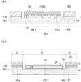
- FIG. 4A is a perspective view of a stiffener 900-1 according to another embodiment, and FIG. 5 shows the stiffener 900-1, the image sensor 810, and the printed circuit board 800 of FIG. 4A .
- the stiffener 900-1 may include a protruding portion 901A disposed in the first region S1 to allow the image sensor to be disposed thereon or attached thereto.
- the protruding portion 901A may include a plurality of protrusions 901-1 to 901-n (n is a natural number, and n > 1) .
- the plurality of protrusions 901-1 to 901-n may be spaced apart from each other, and each of the plurality of protrusions 901-1 to 901-n may protrude in the optical-axis direction on the basis of the upper surface 900a of the second region of the stiffener 901-1.
- An adhesive member 1750a may be disposed between the upper surfaces of the plurality of protrusions 901-1 to 901-n and the lower surface of the image sensor 810.
- the adhesive member 1750a may be disposed between the plurality of protrusions 901-1 to 901-n, or may be charged in the space between the plurality of protrusions 901-1 to 901-n.
- Each of the plurality of protrusions 901-1 to 901-n may have a line shape or a stripe shape, without being limited thereto. In another embodiment, it may be formed in the shape of a net, a plurality of dots, or a plurality of islands.
- FIG. 4B is a perspective view of a stiffener 900-2 according to still another embodiment.
- the stiffener 900-2 may include a protruding portion 902, which includes a plurality of protrusions 902-1 to 902-m (m is a natural number, and m > 1) disposed in the first region S1.
- Each of the plurality of protrusions 902-1 to 902-m may protrude from the upper surface of the stiffener 901-2 in the optical-axis direction.
- Each of the plurality of protrusions 901-2 to 902-m may have a line shape or a stripe shape.
- One ends of the plurality of protrusions 901-2 to 902-m may be connected to each other.
- the opposite ends of the plurality of protrusions 902-1 to 902-m may be connected to each other.
- an adhesive member may be charged in the space between the upper surfaces of the plurality of protrusions 902-1 to 902-m and the lower surface of the image sensor 810 and the space between the plurality of protrusions 902-1 to 902-m.
- the stiffener and the image sensor are fixed to each other using an adhesive member.
- the bonding force between the stiffener and the image sensor may be reduced, which may cause a problem of reliability associated with bonding.
- the area or size of the adhesive is made smaller than the size (or the area) of the lower surface of the image sensor so that the adhesive is placed inside the edge of the lower surface of the image sensor, the flatness of the image sensor is deteriorated during wire bonding, and thus reliability of wire bonding may be deteriorated.
- an uneven portion having a predetermined size is formed on the upper surface of the protruding portion 901A, thereby increasing the bonding area between the adhesive member 1750a and the protruding portion 901A or 902 of the stiffener 900-1 or 900-2, thus increasing bonding force between the stiffener 900-1 or 900-2 and the image sensor 810.
- the convex portions of the uneven portion may be the above-described protrusions 901-1 to 901-n or 902-1 to 902-m, and the concave portions of the uneven portion may be the spaces between the protrusions 901-1 to 901-n or 902-1 to 902-m.
- the convex portions of the uneven portion or the protrusions 901-1 to 901-n or 902-1 to 902-m may suppress overflow of the adhesive, thereby preventing deterioration in the bonding force and preventing the image sensor from being contaminated by the adhesive.
- the edge of the adhesive member 1750a may extend to the edge of the lower surface of the image sensor 810, thereby preventing deterioration in the reliability of wire bonding when wire bonding is performed between the image sensor and the printed circuit board.
- FIG. 6 shows an image sensor 810 and a printed circuit board 800 disposed on a stiffener 900-3 according to still another embodiment.
- the stiffener 900-3 may include a cavity 905 or a recess formed in a first region S1.
- the cavity 905 may have a structure that is recessed from the upper surface of the stiffener 900-3.
- the first region S1 of the stiffener 900-3 may include a cavity 905 that is depressed further than a second region S2 of the stiffener 900-3.
- the image sensor 810 may be disposed in the cavity 905, and may be attached or fixed to a bottom surface 905a of the cavity 905 using an adhesive member 1750.
- the printed circuit board 800 may be disposed in the second region S2 of the stiffener 900-3, and the lower surface of the printed circuit board 800 may be attached or fixed to the second region S2 of the stiffener 900-3 using the adhesive member 1700.
- the bottom surface 905a of the cavity 905 of the stiffener 900-3 of FIG. 6 may be provided with an uneven portion or protrusions (not shown), which are the same as or similar to those described with reference to FIGs. 4A and 4B .
- the image sensor 810 and the printed circuit board 800 may have different thicknesses. That is, the thickness of each of the image sensor and the printed circuit board, which are mounted in the camera module, is not uniform, but may vary according to customers' requests, design specifications, or the size of the camera module.
- the thickness of each of the image sensor and the printed circuit board, which are mounted in the camera module is not uniform, but may vary according to customers' requests, design specifications, or the size of the camera module.
- the depth DT from the upper surface 900a of the stiffener 900-3 to the bottom surface 905a of the cavity 905 may be less than or equal to the thickness T4 of the image sensor (DT ⁇ T4).
- the reason for this is to prevent deterioration in the reliability of wire bonding between the image sensor 810 and the printed circuit board 800 due to an increase in the height difference between the upper surface of the image sensor 810 and the upper surface of the printed circuit board 800 in the optical-axis direction.
- DT may be greater than T4 (DT > T4) depending on the thickness of the image sensor 810 and the thickness of the printed circuit board 800.
- the camera module according to the embodiment may include the stiffener 900, 900-1 or 900-2 of FIG. 3 , 4A or 4B or the stiffener 900-3 of FIG. 6 .
- the embodiment when the thickness T4 of the image sensor 810 is greater than the thickness T3 of the printed circuit board 800 (T4 > T3), the embodiment includes the stiffener 900-3 of FIG. 6 so as to reduce the height difference DP between these two components in the optical-axis direction, thereby preventing deterioration in the reliability of wire bonding.
- the embodiment may include the stiffener 900, 900-1 or 900-2 of FIG. 3 , 4A or 4B so as to reduce the height difference between these two components in the optical-axis direction, thereby preventing deterioration in the reliability of wire bonding.
- FIGs. 7A to 7D show a method of forming the stiffener 900-3 of FIG. 6 .
- a reinforced plate member 90 for forming the stiffener is prepared.
- a first mask 92 or a second mask 92a is formed on the reinforced plate member 90.
- the first mask 92 may be formed on the first region S1, in which the image sensor 810 is to be disposed
- the second mask 92a may be formed on the second region S2, in which the printed circuit board 800 is to be disposed.
- the reinforced plate member 90 is etched using the first mask 92 or the second mask 92a as an etching mask to form the stiffener 900 of FIG. 3 or the stiffener 900-3 of FIG. 6 .
- the stiffener 900-1 or 900-2 of FIG. 4A or 4B may be formed depending on the shape of the pattern of the first mask 92 and the second mask 92a.
- the first mask 92 or the second mask 92a is removed.
- an adhesive member 1700 is attached to the lower surface of the printed circuit board 800.
- the adhesive member 1700 may be attached to the entire area of the lower surface of the printed circuit board 800.
- the ratio of the area of the lower surface of the printed circuit board 800 to the area of the adhesive member 1700 attached to the lower surface of the printed circuit board 800 may be 1:1.
- the thickness of the printed circuit board 800 is expressed differently according to the embodiment 900 or 900-3 of the stiffener.
- an opening 89 is formed so as to penetrate the printed circuit board 800 and the adhesive member 1700 by selectively etching the printed circuit board 800 and the adhesive member 1700 using a mask (not shown) on the printed circuit board 800 to which the adhesive member 1700 has been attached.
- the adhesive member 1700 fixed to the printed circuit board 800 of FIG. 7D is attached to the second region of the stiffener 900 or 900-3.
- the edge of the adhesive member 1700 may extend to the opening 801 in the printed circuit board 800, thereby preventing deterioration in the reliability of wire bonding when wire bonding is performed between the image sensor and the printed circuit board.
- an adhesive member may be formed in the second region of the stiffener of FIG. 7B , and a printed circuit board having therein an opening may be attached to the adhesive member disposed in the second region of the stiffener.
- FIG. 8 is an exploded perspective view of a camera module 200-1 according to another embodiment
- FIG. 9 is a cross-sectional view of the stiffener 900-4, the image sensor 810, and the printed circuit board 800 of FIG. 8 .
- the same reference numerals as those in FIG. 1 denote the same components, and a description of the same components will be omitted or made briefly.
- the stiffener 900-4 includes a first region S1 and a second region S2, and the protruding portion 901 of FIG. 3 or the cavity 905 is not formed in the first region S1 of the stiffener 900-4.
- the first region S1 of the stiffener 900-4 may be a flat surface.
- the printed circuit board 800 is attached to the second region S2 of the stiffener 900-4 using an adhesive member 1700.
- An opening 89 may be formed so as to penetrate the printed circuit board 800 and the adhesive member 1700 to expose the first region S1 of the stiffener 900-4.
- the printed circuit board 800 may have a structure in which a first insulating layer 81-1, a first conductive layer 82-1, a second insulating layer 81-2, a second conductive layer 82-2, and a third insulating layer 81-3 are sequentially stacked.
- the printed circuit board 800 may include at least one terminal 1830, which is disposed on the third insulating layer 81-3 and is electrically connected to at least one of the first conductive layer 82-1 or the second conductive layer.
- the inner surface 17a of the adhesive member 1700 may extend to the inner surface 17b of the opening 801 in the printed circuit board 800.
- the inner surface 17a of the adhesive member 1700 and the inner surface 17b of the opening 801 in the printed circuit board 800 may be positioned in the same plane in the optical-axis direction.
- the adhesive member 1750 disposed in the first region S1 may be spaced apart from the adhesive member 1700 disposed in the second region S2.
- the adhesive member 1750 and the adhesive member 1700 may have different thicknesses from each other, or may be formed through different processes from each other.
- the image sensor 810 is disposed on the first region S1 of the stiffener 900-4, which is exposed through the opening 801, and is attached to the first region S1 using the adhesive member 1750.
- the image sensor 810 may include a terminal 813, which is electrically connected to the terminal 1830 of the printed circuit board 800 via a wire 21.
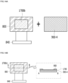
- FIGs. 10A to 10D show a process of coupling the stiffener 900-4, the image sensor 810, the printed circuit board 800, and the adhesive member 1700 shown in FIG. 9 .
- a printed circuit board 800 having therein an opening 801 to expose the image sensor 810 and an adhesive member 1700b having a size corresponding to the size of the printed circuit board 800 are prepared.
- the opening 801 may be a through-hole penetrating the printed circuit board 800.
- the area of the printed circuit board 800 defined by the horizontal length and the vertical length thereof may be the same as the area of the adhesive member 1700 defined by the horizontal length and the vertical length thereof.
- the adhesive member 1700b is attached to the lower surface of the printed circuit board 800 having therein the opening 801.
- a portion of the adhesive member 1700b attached to the lower surface of the printed circuit board 800 may be exposed through the opening 801 in the printed circuit board 800.
- the area of the adhesive member 1700b exposed through the opening 801 may be the same as the area of the opening 801.
- the region 1700a of the adhesive member 1700b that is exposed through the opening 801 is removed through an etching process using a mask to form an adhesive member 1700 having therein an opening, and the mask is removed.
- An opening 89 may be formed so as to penetrate the printed circuit board 800 and the adhesive member 1700 through the processing of FIG. 10C .
- the adhesive member 1700 is attached to the stiffener 900-4.
- the first region S1 of the stiffener 900-4 may be exposed through the opening 89.
- the image sensor 810 is disposed or mounted in the first region S1 of the stiffener 900-4.
- the image sensor 810 may be attached to the first region S1 of the stiffener 900-4 using the adhesive member 1750.
- a wire connecting the terminal of the printed circuit board 800 to the terminal of the image sensor 810 is formed through a wire-bonding process.
- the embodiment is capable of preventing the generation of an unfilled region between the lower surface of the printed circuit board 800 and the second region S2 of the stiffener 900-4, in which the adhesive member 1700 is not charged.
- the adhesive is attached to the printed circuit board so as to be spaced inwards apart from the inner surface of the opening in the printed circuit board by 200 [pm] to 300 [pm].
- the adhesive is attached to the printed circuit board so as to be spaced inwards apart from the inner surface of the opening in the printed circuit board by 200 [pm] to 300 [pm]
- an unfilled region, in which the adhesive is not charged, is generated between the printed circuit board and the stiffener, which may cause warpage of the printed circuit board, and when wire bonding is performed between the warped printed circuit board and the image sensor, the reliability of wire bonding may be deteriorated.
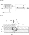
- FIG. 11 shows wire bonding between a printed circuit board 32 and an image sensor 33 when a region 12-1 in which an adhesive is not charged is present.
- a region 12-1 in which the adhesive 30 is not charged may be formed between the printed circuit board 32 and the stiffener 31, and the printed circuit board 30 may be warped due to the presence of the region 12-1 in which the adhesive 30 is not charged.
- FIG. 12 shows simulation results pertaining to a height difference caused by warpage of the printed circuit board 32 shown in FIG. 11 , which occurs due to the force applied thereto during wire bonding, and the height difference caused by warpage of the printed circuit board 800 according to the embodiment of FIG. 9 , which occurs due to the force applied thereto during wire bonding.
- the height difference in FIG. 12 may be the height difference from one end of the printed circuit board 32 to the opposite end thereof, which is indicated by F1.
- the height difference in FIG. 12 may be the height difference between the highest point of the printed circuit board and the lowest point thereof.
- the X-axis represents the force applied to the printed circuit board 32 or 800 by the wire-bonding apparatus, and the unit of force may be [g-cm/s ⁇ 2].
- the Y-axis represents the height difference, and the unit thereof may be micrometers.
- g1 represents the height difference caused by warpage of the printed circuit board 32
- g2 represents the height difference caused by warpage of the printed circuit board 800.
- the height difference g1 increases, but even when the force applied to the printed circuit board 800 increases, the height difference g2 may be constant.
- the printed circuit board 800 is warped insignificantly during wire bonding, and thus the height difference is constant, thereby securing reliability of wire bonding between the printed circuit board 800 and the image sensor 810.
- FIG. 13 is a cross-sectional view of other embodiments of the stiffener 900-4, the image sensor 810, and the printed circuit board 800 of FIG. 8 .
- the same reference numerals as those in FIG. 8 denote the same components, and a description of the same components will be omitted or made briefly.
- the printed circuit board 800 and the image sensor 810 may be attached to the stiffener 900-4 using one adhesive member 1700b.
- the adhesive member 1700b may include a first adhesive member 1700b1 disposed in a first region S1 of the stiffener 900-4 and a second adhesive member 1700b2 disposed in a second region S2 of the stiffener 900-4 and connected to or contiguous with the first adhesive member 1700b1.
- the first adhesive member 1700b1 may be in contact with the opening 801 in the printed circuit board 800 along the inner surface of the opening 801 in the printed circuit board 800.
- the adhesive member 1700b may cover the entire area of the first region S1 of the stiffener 900-4.
- the upper surface of the first adhesive member 1700b1 and the upper surface of the second adhesive member 1700b2 may be positioned in the same plane.
- FIGs. 14A and 14B show a process of coupling the stiffener 900-4, the image sensor 810, the printed circuit board 800, and the adhesive member 1700b shown in FIG. 13 .
- the adhesive member 1700b is attached to the lower surface of the printed circuit board 800 having therein the opening 801.
- the adhesive member 1700b is attached to the upper surface of the stiffener 900-4.
- the adhesive member 1700b may cover both the first region S1 and the second region S2 of the stiffener 900-4.
- the adhesive member 1700b may include a first adhesive member 1700b1 covering the entire area of the first region S1 of the stiffener 900-4 and a second adhesive member 1700b2 covering the entire area of the second region S2 of the stiffener 900-4.
- the first adhesive member 1700b1 may be exposed through the opening 801 in the printed circuit board 800.
- the image sensor 810 is disposed or mounted on the first adhesive member 1700b1, exposed through the opening 801 in the printed circuit board 800.
- a wire connecting the terminal of the printed circuit board 800 to the terminal of the image sensor 810 is formed through a wire-bonding process.
- the camera module 200 may include a printed circuit board 800 having therein an opening 801 to allow the image sensor 810 to be disposed therein in order to reduce the height of the camera module 200.
- the camera module 200 may include a stiffener 900, which supports the printed circuit board 800 and on which the image sensor 810 is mounted in order to dissipate the heat generated from the image sensor 810.
- the height of the camera module is proportional to the thickness of the stiffener.
- the flatness of the stiffener 900, on which the image sensor is mounted may be deteriorated, and the optical performance of the camera module may be deteriorated.
- the embodiment includes the stiffener 900 having the protruding portion 901, on which the image sensor 810 is mounted, thereby improving the flatness of the stiffener 900, thus improving the optical performance of the camera module.
- the embodiment selectively adopts the shape of the stiffener of the embodiment of FIG. 3 or the shape of the stiffener of the embodiment of FIG. 6 depending on the thickness of the image sensor and the thickness of the printed circuit board, thereby reducing the height difference between the image sensor 810 and the printed circuit board 800 in the optical-axis direction, thus securing reliability of wire bonding.
- an uneven portion is formed on the protruding portion 901 of the stiffener 900, on which the image sensor is mounted, thereby increasing the bonding force between the stiffener and the image sensor and preventing deterioration in the bonding force and contamination of the image sensor due to overflow of the adhesive.
- the printed circuit board 800, the stiffener 900, the image sensor 810, and the adhesive member 1700 or 1700b are coupled through the method of FIGs. 7A to 7E , FIGs. 10A to 10D , or FIGs. 14A and 14B .
- the adhesive member 1700 or 1700b are coupled through the method of FIGs. 7A to 7E , FIGs. 10A to 10D , or FIGs. 14A and 14B .
- the camera module according to the embodiment may be included in an optical instrument for the purpose of forming an image of an object present in a space using reflection, refraction, absorption, interference, and diffraction, which are characteristics of light, for the purpose of increasing visibility, for the purpose of recording and reproduction of an image by a lens, or for the purpose of optical measurement or image propagation or transmission.
- the optical instrument according to the embodiment may include a smartphone and a portable terminal equipped with a camera.
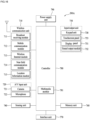
- FIG. 15 is a perspective view of a portable terminal 200A according to an embodiment
- FIG. 16 is a configuration diagram of the portable terminal 200A shown in FIG. 15 .
- the portable terminal 200A may include a body 850, a wireless communication unit 710, an A/V input unit 720, a sensor 740, an input/output unit 750, a memory 760, an interface 770, a controller 780, and a power supply 790.
- the body 850 shown in FIG. 15 has a bar shape, without being limited thereto, and may be any of various types such as, for example, a slide type, a folder type, a swing type, or a swivel type, in which two or more sub-bodies are coupled so as to be movable relative to each other.
- the body 850 may include a case (e.g. casing, housing, or cover) defining the external appearance thereof.
- the body 850 may be divided into a front case 851 and a rear case 852.
- a variety of electronic components of the terminal may be mounted in the space formed between the front case 851 and the rear case 852.
- the wireless communication unit 710 may include one or more modules, which enable wireless communication between the terminal 200A and a wireless communication system or between the terminal 200A and a network in which the terminal 200A is located.
- the wireless communication unit 710 may include a broadcast receiving module 711, a mobile communication module 712, a wireless Internet module 713, a nearfield communication module 714, and a location information module 715.
- the audio/video (A/V) input unit 720 serves to input audio signals or video signals, and may include a camera 721 and a microphone 722.
- the camera 721 may include the camera module 200 or 200-1 according to the embodiment shown in FIG. 1 or 8 .
- the sensor 740 may sense the current state of the terminal 200A, such as the open or closed state of the terminal 200A, the location of the terminal 200A, the presence or absence of a user's touch, the orientation of the terminal 200A, or the acceleration/deceleration of the terminal 200A, and may generate a sensing signal to control the operation of the terminal 200A. For example, when the terminal 200A is a slide-type phone, whether the slide-type phone is open or closed may be detected. In addition, the sensor 740 serves to sense whether power is supplied from the power supply 790 or whether the interface 770 is coupled to an external device.
- the input/output unit 750 serves to generate visual, audible, or tactile input or output.
- the input/output unit 750 may generate input data to control the operation of the terminal 200A, and may display information processed in the terminal 200A.
- the input/output unit 750 may include a keypad unit 730, a display panel 751, a sound output module 752, and a touchscreen panel 753.
- the keypad unit 730 may generate input data in response to input to a keypad.
- the display panel 751 may include a plurality of pixels, the color of which varies in response to electrical signals.
- the display panel 751 may include at least one of a liquid crystal display, a thin-film transistor liquid crystal display, an organic light-emitting diode, a flexible display, or a 3D display.
- the sound output module 752 may output audio data received from the wireless communication unit 710 in a call-signal reception mode, a call mode, a recording mode, a voice recognition mode, or a broadcast reception mode, or may output audio data stored in the memory 760.
- the touchscreen panel 753 may convert variation in capacitance, caused by a user's touch on a specific region of a touchscreen, into electrical input signals.
- the memory 760 may store programs for the processing and control of the controller 780, and may temporarily store input/output data (e.g. a phone book, messages, audio, still images, pictures, and moving images).
- input/output data e.g. a phone book, messages, audio, still images, pictures, and moving images.
- the memory 760 may store images captured by the camera 721, for example, pictures or moving images.
- the interface 770 serves as a passage for connection between the terminal 200A and an external device.
- the interface 770 may receive data or power from the external device, and may transmit the same to respective components inside the terminal 200A, or may transmit data inside the terminal 200A to the external device.
- the interface 770 may include a wired/wireless headset port, an external charger port, a wired/wireless data port, a memory card port, a port for connection of a device having an identification module, an audio input/output (I/O) port, a video input/output (I/O) port, and an earphone port.
- the controller 780 may control the general operation of the terminal 200A.
- the controller 780 may perform control and processing related to voice calls, data communication, and video calls.
- the controller 780 may include a multimedia module 781 for multimedia playback.
- the multimedia module 781 may be provided inside the controller 180, or may be provided separately from the controller 780.
- the controller 780 may perform pattern recognition processing, by which writing or drawing input to the touchscreen is perceived as characters or images.
- the power supply 790 may supply power required to operate the respective components upon receiving external power or internal power under the control of the controller 780.
- the embodiments may be used in a camera module and an optical device capable of improving optical performance, securing reliability of wire bonding between a printed circuit board and an image sensor, and increasing bonding force between a stiffener and the image sensor.
- a camera module comprising:
- a camera module comprising:
- a camera module comprising:
Landscapes
- Physics & Mathematics (AREA)
- Engineering & Computer Science (AREA)
- Multimedia (AREA)
- Signal Processing (AREA)
- General Physics & Mathematics (AREA)
- Optics & Photonics (AREA)
- Electromagnetism (AREA)
- Studio Devices (AREA)
- Blocking Light For Cameras (AREA)
- Transforming Light Signals Into Electric Signals (AREA)
Applications Claiming Priority (3)
| Application Number | Priority Date | Filing Date | Title |
|---|---|---|---|
| KR1020180031895A KR102492626B1 (ko) | 2018-03-20 | 2018-03-20 | 카메라 모듈 및 이를 포함하는 광학 기기 |
| EP19771520.4A EP3771195B1 (fr) | 2018-03-20 | 2019-03-18 | Module de caméra et dispositif optique le comprenant |
| PCT/KR2019/003108 WO2019182307A1 (fr) | 2018-03-20 | 2019-03-18 | Module de caméra et dispositif optique le comprenant |
Related Parent Applications (1)
| Application Number | Title | Priority Date | Filing Date |
|---|---|---|---|
| EP19771520.4A Division EP3771195B1 (fr) | 2018-03-20 | 2019-03-18 | Module de caméra et dispositif optique le comprenant |
Publications (2)
| Publication Number | Publication Date |
|---|---|
| EP4485957A2 true EP4485957A2 (fr) | 2025-01-01 |
| EP4485957A3 EP4485957A3 (fr) | 2025-03-12 |
Family
ID=67987414
Family Applications (2)
| Application Number | Title | Priority Date | Filing Date |
|---|---|---|---|
| EP19771520.4A Active EP3771195B1 (fr) | 2018-03-20 | 2019-03-18 | Module de caméra et dispositif optique le comprenant |
| EP24213360.1A Pending EP4485957A3 (fr) | 2018-03-20 | 2019-03-18 | Module de caméra et dispositif optique le comprenant |
Family Applications Before (1)
| Application Number | Title | Priority Date | Filing Date |
|---|---|---|---|
| EP19771520.4A Active EP3771195B1 (fr) | 2018-03-20 | 2019-03-18 | Module de caméra et dispositif optique le comprenant |
Country Status (5)
| Country | Link |
|---|---|
| US (3) | US11418687B2 (fr) |
| EP (2) | EP3771195B1 (fr) |
| KR (3) | KR102492626B1 (fr) |
| CN (2) | CN112154645B (fr) |
| WO (1) | WO2019182307A1 (fr) |
Families Citing this family (18)
| Publication number | Priority date | Publication date | Assignee | Title |
|---|---|---|---|---|
| CN211481581U (zh) * | 2019-12-10 | 2020-09-11 | 广州立景创新科技有限公司 | 嵌入式补强线路板、摄像模块和电子装置 |
| KR102423617B1 (ko) * | 2020-06-04 | 2022-07-22 | (주)파트론 | 광학식 지문 인식 센서 모듈 및 이를 적용한 전자 장치 |
| KR20220026792A (ko) * | 2020-08-26 | 2022-03-07 | 엘지이노텍 주식회사 | 카메라 모듈 및 이를 포함하는 광학기기 |
| KR102879016B1 (ko) * | 2020-08-28 | 2025-10-29 | 엘지이노텍 주식회사 | 이미지 센서 패키지 및 이를 포함하는 카메라 장치 |
| KR102944479B1 (ko) | 2020-12-28 | 2026-03-26 | 엘지이노텍 주식회사 | 카메라 모듈 및 이를 포함하는 광학기기 |
| KR20220093539A (ko) * | 2020-12-28 | 2022-07-05 | 엘지이노텍 주식회사 | 카메라 모듈 및 이를 포함하는 광학기기 |
| KR20220107609A (ko) | 2021-01-25 | 2022-08-02 | 엘지이노텍 주식회사 | 카메라 모듈 및 이를 포함하는 광학기기 |
| CN112859277B (zh) * | 2021-02-26 | 2022-08-02 | 广州立景创新科技有限公司 | 镜头模块 |
| TWI783388B (zh) * | 2021-02-26 | 2022-11-11 | 大陸商廣州立景創新科技有限公司 | 鏡頭模組 |
| KR102897964B1 (ko) | 2021-06-08 | 2025-12-09 | 삼성전자주식회사 | 카메라 모듈 및 그것을 포함하는 전자 장치 |
| KR102913021B1 (ko) * | 2021-06-30 | 2026-01-15 | 엘지이노텍 주식회사 | 카메라 장치 |
| KR102899639B1 (ko) | 2021-07-06 | 2025-12-15 | 삼성전자주식회사 | 카메라 모듈을 포함하는 전자 장치 |
| CN118044212A (zh) | 2021-11-10 | 2024-05-14 | 三星电子株式会社 | 相机模块和包括相机模块的电子装置 |
| KR20230068114A (ko) * | 2021-11-10 | 2023-05-17 | 삼성전자주식회사 | 카메라 모듈 및 이를 포함하는 전자 장치 |
| WO2023130196A1 (fr) * | 2022-01-04 | 2023-07-13 | Suzhou Xpectvision IM Technology Co., Ltd. | Capteurs d'images multicouches |
| US20250024149A1 (en) * | 2022-01-27 | 2025-01-16 | Lg Innotek Co., Ltd. | Camera device |
| US20250184588A1 (en) * | 2022-03-02 | 2025-06-05 | Lg Innotek Co., Ltd. | Camera module |
| US12229627B1 (en) * | 2023-08-01 | 2025-02-18 | Datalogic Ip Tech S.R.L. | Scanner camera with PCB-integrated lens holder |
Family Cites Families (32)
| Publication number | Priority date | Publication date | Assignee | Title |
|---|---|---|---|---|
| US6956615B2 (en) * | 2000-01-28 | 2005-10-18 | Pentax Corporation | Structure for mounting a solid-state imaging device |
| JP3607160B2 (ja) * | 2000-04-07 | 2005-01-05 | 三菱電機株式会社 | 撮像装置 |
| JP4405062B2 (ja) * | 2000-06-16 | 2010-01-27 | 株式会社ルネサステクノロジ | 固体撮像装置 |
| US6784534B1 (en) * | 2002-02-06 | 2004-08-31 | Amkor Technology, Inc. | Thin integrated circuit package having an optically transparent window |
| AU2003281651A1 (en) | 2002-07-18 | 2004-02-09 | Koninklijke Philips Electronics N.V. | Camera module, holder for use in a camera module, camera system and method of manufacturing a camera module |
| KR100815325B1 (ko) | 2006-07-31 | 2008-03-19 | 삼성전기주식회사 | 모바일 기기용 카메라 모듈 |
| KR101327622B1 (ko) * | 2007-03-30 | 2013-11-12 | 엘지이노텍 주식회사 | 카메라 모듈 |
| KR100780204B1 (ko) * | 2006-12-13 | 2007-11-27 | 삼성전기주식회사 | 접지용 더미기판을 갖는 카메라 모듈 |
| CN100576555C (zh) * | 2007-08-09 | 2009-12-30 | 佛山普立华科技有限公司 | 影像装置 |
| KR101449006B1 (ko) * | 2007-11-29 | 2014-10-08 | 엘지이노텍 주식회사 | 카메라 모듈 |
| US8432485B1 (en) * | 2007-12-19 | 2013-04-30 | Logitech Europe S.A. | Optimized designs for embedding webcam modules with superior image quality in electronics displays |
| JP5324935B2 (ja) * | 2009-01-20 | 2013-10-23 | 株式会社ザクティ | 固体撮像装置 |
| WO2011086713A1 (fr) | 2010-01-15 | 2011-07-21 | 京進工業株式会社 | Appareil de fabrication d'échangeur de chaleur |
| KR101711007B1 (ko) * | 2010-04-29 | 2017-03-02 | 삼성전자주식회사 | 이미지 센서 패키지를 갖는 이미지 센서 모듈 |
| KR101795739B1 (ko) | 2010-09-17 | 2017-12-01 | 엘지이노텍 주식회사 | 카메라 모듈 및 그 제조 방법 |
| KR101834953B1 (ko) | 2010-11-18 | 2018-03-06 | 엘지이노텍 주식회사 | 카메라 모듈 |
| EP2641391B1 (fr) | 2010-11-18 | 2017-10-18 | LG Innotek Co., Ltd. | Module d'appareil de prise de vues et son procédé de fabrication |
| US8605211B2 (en) * | 2011-04-28 | 2013-12-10 | Apple Inc. | Low rise camera module |
| US9136289B2 (en) * | 2011-08-23 | 2015-09-15 | Flextronics Ap, Llc | Camera module housing having built-in conductive traces to accommodate stacked dies using flip chip connections |
| KR101300316B1 (ko) * | 2011-09-23 | 2013-08-28 | 삼성전기주식회사 | 카메라모듈 |
| KR20130038630A (ko) * | 2011-10-10 | 2013-04-18 | 삼성전기주식회사 | 카메라모듈 |
| CN104798364B (zh) * | 2012-06-07 | 2018-08-17 | 数位光学欧洲有限公司 | Mems快速对焦照相机模块 |
| US8866246B2 (en) * | 2012-11-01 | 2014-10-21 | Larview Technologies Corporation | Holder on chip module structure |
| CN104284060B (zh) * | 2013-07-12 | 2019-07-02 | 鸿富锦精密工业(深圳)有限公司 | 相机模组 |
| US9241097B1 (en) * | 2013-09-27 | 2016-01-19 | Amazon Technologies, Inc. | Camera module including image sensor die in molded cavity substrate |
| JP2015177310A (ja) * | 2014-03-14 | 2015-10-05 | 株式会社東芝 | カメラモジュール |
| CN104749858A (zh) * | 2015-03-12 | 2015-07-01 | 南昌欧菲光电技术有限公司 | 摄像头模组的支架及摄像头模组 |
| WO2016200126A1 (fr) * | 2015-06-08 | 2016-12-15 | 엘지이노텍(주) | Module d'appareil photographique |
| US10187560B2 (en) * | 2015-10-15 | 2019-01-22 | Omnivision Technologies, Inc. | Notched-spacer camera module and method for fabricating same |
| CN106803870B (zh) | 2015-11-26 | 2022-01-04 | 三星电机株式会社 | 相机模块 |
| CN205179201U (zh) * | 2015-12-07 | 2016-04-20 | 南昌欧菲光电技术有限公司 | 具有摄像头模组的电子设备 |
| CN205883388U (zh) * | 2016-07-20 | 2017-01-11 | 新科实业有限公司 | 透镜组件及相机模组 |
-
2018
- 2018-03-20 KR KR1020180031895A patent/KR102492626B1/ko active Active
-
2019
- 2019-03-18 WO PCT/KR2019/003108 patent/WO2019182307A1/fr not_active Ceased
- 2019-03-18 EP EP19771520.4A patent/EP3771195B1/fr active Active
- 2019-03-18 EP EP24213360.1A patent/EP4485957A3/fr active Pending
- 2019-03-18 CN CN201980034275.8A patent/CN112154645B/zh active Active
- 2019-03-18 US US16/982,504 patent/US11418687B2/en active Active
- 2019-03-18 CN CN202211237602.XA patent/CN115866375A/zh active Pending
-
2022
- 2022-07-14 US US17/864,680 patent/US11706519B2/en active Active
-
2023
- 2023-01-19 KR KR1020230007993A patent/KR102775846B1/ko active Active
- 2023-05-30 US US18/203,483 patent/US12108137B2/en active Active
-
2025
- 2025-02-20 KR KR1020250022506A patent/KR20250029837A/ko active Pending
Also Published As
| Publication number | Publication date |
|---|---|
| CN112154645B (zh) | 2022-10-25 |
| KR102775846B1 (ko) | 2025-03-07 |
| US20230328352A1 (en) | 2023-10-12 |
| US11706519B2 (en) | 2023-07-18 |
| CN115866375A (zh) | 2023-03-28 |
| WO2019182307A1 (fr) | 2019-09-26 |
| US20220353396A1 (en) | 2022-11-03 |
| US12108137B2 (en) | 2024-10-01 |
| US11418687B2 (en) | 2022-08-16 |
| KR20250029837A (ko) | 2025-03-05 |
| KR102492626B1 (ko) | 2023-01-27 |
| EP3771195A1 (fr) | 2021-01-27 |
| EP3771195A4 (fr) | 2021-12-08 |
| KR20230017334A (ko) | 2023-02-03 |
| CN112154645A (zh) | 2020-12-29 |
| EP4485957A3 (fr) | 2025-03-12 |
| KR20190110226A (ko) | 2019-09-30 |
| US20210021744A1 (en) | 2021-01-21 |
| EP3771195B1 (fr) | 2024-12-18 |
Similar Documents
| Publication | Publication Date | Title |
|---|---|---|
| US11706519B2 (en) | Camera module and optical device comprising same | |
| US12457396B2 (en) | Camera module and optical device including same | |
| US12393100B2 (en) | Camera module and optical device comprising same | |
| US12212829B2 (en) | Camera module and optical instrument comprising same | |
| KR102508493B1 (ko) | 카메라 모듈 및 이를 포함하는 광학 기기 | |
| EP4123369B1 (fr) | Dispositif d'entraînement de lentille, ainsi que module de caméra et dispositif optique le comprenant | |
| US12345854B2 (en) | Protective sheet and camera module comprising same | |
| KR20210121785A (ko) | 카메라 모듈 및 이를 포함하는 광학 기기 |
Legal Events
| Date | Code | Title | Description |
|---|---|---|---|
| PUAI | Public reference made under article 153(3) epc to a published international application that has entered the european phase |
Free format text: ORIGINAL CODE: 0009012 |
|
| STAA | Information on the status of an ep patent application or granted ep patent |
Free format text: STATUS: THE APPLICATION HAS BEEN PUBLISHED |
|
| AC | Divisional application: reference to earlier application |
Ref document number: 3771195 Country of ref document: EP Kind code of ref document: P |
|
| AK | Designated contracting states |
Kind code of ref document: A2 Designated state(s): AL AT BE BG CH CY CZ DE DK EE ES FI FR GB GR HR HU IE IS IT LI LT LU LV MC MK MT NL NO PL PT RO RS SE SI SK SM TR |
|
| REG | Reference to a national code |
Ref country code: DE Ref legal event code: R079 Free format text: PREVIOUS MAIN CLASS: H04N0023680000 Ipc: H04N0023540000 |
|
| PUAL | Search report despatched |
Free format text: ORIGINAL CODE: 0009013 |
|
| AK | Designated contracting states |
Kind code of ref document: A3 Designated state(s): AL AT BE BG CH CY CZ DE DK EE ES FI FR GB GR HR HU IE IS IT LI LT LU LV MC MK MT NL NO PL PT RO RS SE SI SK SM TR |
|
| RIC1 | Information provided on ipc code assigned before grant |
Ipc: G03B 30/00 20210101ALI20250131BHEP Ipc: G03B 17/02 20210101ALI20250131BHEP Ipc: H04N 23/68 20230101ALI20250131BHEP Ipc: H04N 23/57 20230101ALI20250131BHEP Ipc: H04N 23/54 20230101AFI20250131BHEP |
|
| STAA | Information on the status of an ep patent application or granted ep patent |
Free format text: STATUS: REQUEST FOR EXAMINATION WAS MADE |
|
| 17P | Request for examination filed |
Effective date: 20250909 |
|
| STAA | Information on the status of an ep patent application or granted ep patent |
Free format text: STATUS: EXAMINATION IS IN PROGRESS |
|
| 17Q | First examination report despatched |
Effective date: 20260324 |