EP4489082A1 - Solarzelle und herstellungsverfahren dafür - Google Patents
Solarzelle und herstellungsverfahren dafür Download PDFInfo
- Publication number
- EP4489082A1 EP4489082A1 EP23869677.7A EP23869677A EP4489082A1 EP 4489082 A1 EP4489082 A1 EP 4489082A1 EP 23869677 A EP23869677 A EP 23869677A EP 4489082 A1 EP4489082 A1 EP 4489082A1
- Authority
- EP
- European Patent Office
- Prior art keywords
- doped
- wafer substrate
- film layer
- boron
- phosphorus
- Prior art date
- Legal status (The legal status is an assumption and is not a legal conclusion. Google has not performed a legal analysis and makes no representation as to the accuracy of the status listed.)
- Pending
Links
Images


Classifications
-
- H—ELECTRICITY
- H10—SEMICONDUCTOR DEVICES; ELECTRIC SOLID-STATE DEVICES NOT OTHERWISE PROVIDED FOR
- H10F—INORGANIC SEMICONDUCTOR DEVICES SENSITIVE TO INFRARED RADIATION, LIGHT, ELECTROMAGNETIC RADIATION OF SHORTER WAVELENGTH OR CORPUSCULAR RADIATION
- H10F71/00—Manufacture or treatment of devices covered by this subclass
- H10F71/121—The active layers comprising only Group IV materials
- H10F71/1221—The active layers comprising only Group IV materials comprising polycrystalline silicon
-
- H—ELECTRICITY
- H10—SEMICONDUCTOR DEVICES; ELECTRIC SOLID-STATE DEVICES NOT OTHERWISE PROVIDED FOR
- H10F—INORGANIC SEMICONDUCTOR DEVICES SENSITIVE TO INFRARED RADIATION, LIGHT, ELECTROMAGNETIC RADIATION OF SHORTER WAVELENGTH OR CORPUSCULAR RADIATION
- H10F10/00—Individual photovoltaic cells, e.g. solar cells
- H10F10/10—Individual photovoltaic cells, e.g. solar cells having potential barriers
- H10F10/16—Photovoltaic cells having only PN heterojunction potential barriers
- H10F10/164—Photovoltaic cells having only PN heterojunction potential barriers comprising heterojunctions with Group IV materials, e.g. ITO/Si or GaAs/SiGe photovoltaic cells
- H10F10/165—Photovoltaic cells having only PN heterojunction potential barriers comprising heterojunctions with Group IV materials, e.g. ITO/Si or GaAs/SiGe photovoltaic cells the heterojunctions being Group IV-IV heterojunctions, e.g. Si/Ge, SiGe/Si or Si/SiC photovoltaic cells
-
- H—ELECTRICITY
- H10—SEMICONDUCTOR DEVICES; ELECTRIC SOLID-STATE DEVICES NOT OTHERWISE PROVIDED FOR
- H10F—INORGANIC SEMICONDUCTOR DEVICES SENSITIVE TO INFRARED RADIATION, LIGHT, ELECTROMAGNETIC RADIATION OF SHORTER WAVELENGTH OR CORPUSCULAR RADIATION
- H10F77/00—Constructional details of devices covered by this subclass
- H10F77/10—Semiconductor bodies
- H10F77/12—Active materials
- H10F77/122—Active materials comprising only Group IV materials
- H10F77/1223—Active materials comprising only Group IV materials characterised by the dopants
-
- H—ELECTRICITY
- H10—SEMICONDUCTOR DEVICES; ELECTRIC SOLID-STATE DEVICES NOT OTHERWISE PROVIDED FOR
- H10F—INORGANIC SEMICONDUCTOR DEVICES SENSITIVE TO INFRARED RADIATION, LIGHT, ELECTROMAGNETIC RADIATION OF SHORTER WAVELENGTH OR CORPUSCULAR RADIATION
- H10F77/00—Constructional details of devices covered by this subclass
- H10F77/20—Electrodes
- H10F77/206—Electrodes for devices having potential barriers
- H10F77/211—Electrodes for devices having potential barriers for photovoltaic cells
- H10F77/219—Arrangements for electrodes of back-contact photovoltaic cells
-
- H—ELECTRICITY
- H10—SEMICONDUCTOR DEVICES; ELECTRIC SOLID-STATE DEVICES NOT OTHERWISE PROVIDED FOR
- H10F—INORGANIC SEMICONDUCTOR DEVICES SENSITIVE TO INFRARED RADIATION, LIGHT, ELECTROMAGNETIC RADIATION OF SHORTER WAVELENGTH OR CORPUSCULAR RADIATION
- H10F77/00—Constructional details of devices covered by this subclass
- H10F77/30—Coatings
- H10F77/306—Coatings for devices having potential barriers
- H10F77/311—Coatings for devices having potential barriers for photovoltaic cells
- H10F77/315—Coatings for devices having potential barriers for photovoltaic cells the coatings being antireflective or having enhancing optical properties
-
- H—ELECTRICITY
- H10—SEMICONDUCTOR DEVICES; ELECTRIC SOLID-STATE DEVICES NOT OTHERWISE PROVIDED FOR
- H10F—INORGANIC SEMICONDUCTOR DEVICES SENSITIVE TO INFRARED RADIATION, LIGHT, ELECTROMAGNETIC RADIATION OF SHORTER WAVELENGTH OR CORPUSCULAR RADIATION
- H10F77/00—Constructional details of devices covered by this subclass
- H10F77/70—Surface textures, e.g. pyramid structures
- H10F77/703—Surface textures, e.g. pyramid structures of the semiconductor bodies, e.g. textured active layers
-
- Y—GENERAL TAGGING OF NEW TECHNOLOGICAL DEVELOPMENTS; GENERAL TAGGING OF CROSS-SECTIONAL TECHNOLOGIES SPANNING OVER SEVERAL SECTIONS OF THE IPC; TECHNICAL SUBJECTS COVERED BY FORMER USPC CROSS-REFERENCE ART COLLECTIONS [XRACs] AND DIGESTS
- Y02—TECHNOLOGIES OR APPLICATIONS FOR MITIGATION OR ADAPTATION AGAINST CLIMATE CHANGE
- Y02P—CLIMATE CHANGE MITIGATION TECHNOLOGIES IN THE PRODUCTION OR PROCESSING OF GOODS
- Y02P70/00—Climate change mitigation technologies in the production process for final industrial or consumer products
- Y02P70/50—Manufacturing or production processes characterised by the final manufactured product
Definitions
- the present application relates to the technical field of solar cells, and in particular to a solar cell and a method for preparing the same.
- crystalline silicon solar cells such as a passivated emitter and rear cell (PERC), a tunnel oxide passivated contact (TOPCon) solar cell, and an interdigitated back contact (IBC) cell
- PERC passivated emitter and rear cell
- TOPCon tunnel oxide passivated contact
- IBC interdigitated back contact
- a front surface of a cell needs to be prepared as a textured surface, and a back surface is a polished structure.
- a conventional practice is to first polish both surfaces in a wet groove, next design a mask layer to serve as a barrier on the back surface of the cell, and then enter the wet groove, thereby achieving a textured front surface and a polished back surface.
- the back surface needs to be designed with grooves or patterns, and a mask structure is also needed.
- a wrap-around layer is formed on the front surface of the silicon wafer, and it is also necessary to provide a mask layer on the back surface and then remove the wrap-around layer on the front surface.
- a mask layer used in a conventional solar cell production process exhibits insufficient corrosion resistance, resulting in a short time window for processes such as texturing or wrap-around removal, and affecting the yield of cells.
- a method for preparing a solar cell includes the following steps of:
- the solar cell substrate is a silicon wafer substrate
- the area A includes a front surface of the silicon wafer substrate and a partial area of a back surface of the silicon wafer substrate
- the area B is an area of the back surface of the silicon wafer substrate that does not belong to the area A.
- the first treatment includes performing the texturing process on the area A of the front surface of the silicon wafer substrate with a chemical liquid for texturing, and performing an etching process on the area A of the back surface of the silicon wafer substrate.
- forming the phosphorous-boron co-doped silicon oxide layer on the area B includes the following steps of:
- forming the phosphorous-boron co-doped silicon oxide layer on the back surface of the silicon wafer substrate includes the following steps of:
- the phosphorus-doped amorphous silicon film layer and the boron-doped silicon oxide layer are sequentially formed on the back surface of the silicon wafer substrate through plasma enhanced chemical vapor deposition.
- forming the phosphorus-doped amorphous silicon film layer includes the following step of: depositing the phosphorus-doped amorphous silicon film layer on the back surface of the silicon wafer substrate through plasma enhanced chemical vapor deposition by using a reaction gas containing phosphorane and silane, wherein during depositing the phosphorus-doped amorphous silicon film layer, a flow rate of the phosphorane in the reaction gas gradually increase.
- forming the boron-doped silicon oxide layer includes the following step of: depositing the boron-doped silicon oxide layer on the back surface of the silicon wafer substrate by plasma enhanced chemical vapor deposition by using a reaction gas containing a boron source and silane, wherein during depositing the boron-doped silicon oxide layer, a flow rate of the boron source in the reaction gas is lower than 1/3 of a flow rate of the silane.
- an annealing temperature is 800°C to 950°C, and an annealing time is 15 min to 60 min.
- forming the phosphorous-boron co-doped silicon oxide layer on the back surface of the silicon wafer substrate includes the following steps of:
- the patterning includes the following step of: treating the back surface of the silicon wafer substrate with a green laser or an ultraviolet laser to remove the part of the phosphorous-boron co-doped silicon oxide layer.
- the method further includes the following step of: forming an ultra-thin silicon oxide layer on the back surface of the silicon wafer substrate through plasma enhanced chemical vapor deposition, wherein the ultra-thin silicon oxide layer has a thickness from 1 nm to 3 nm.
- the method further includes the following steps of:
- the method further includes the following step of: depositing a first aluminum oxide film layer and a second aluminum oxide film layer on the front surface and the back surface of the silicon wafer substrate, respectively.
- the method further includes the following step of: depositing a first anti-reflection film layer and a second anti-reflection film layer on the first aluminum oxide film layer and the second aluminum oxide film layer, respectively.
- the solar cell substrate is a silicon wafer substrate with a wrap-around layer on the front surface thereof; the area A includes the front surface of the silicon wafer substrate, and the area B includes a back surface of the silicon wafer substrate; and the first treatment is the wrap-around removal process on the area A.
- forming the phosphorous-boron co-doped silicon oxide layer on the area B includes the following steps of:
- the phosphorus-doped amorphous silicon film layer and the boron-doped silicon oxide layer are sequentially formed on the back surface of the silicon wafer substrate through plasma enhanced chemical vapor deposition.
- forming the phosphorus-doped amorphous silicon film layer includes the following step of: depositing the phosphorus-doped amorphous silicon film layer on the back surface of the silicon wafer substrate through plasma enhanced chemical vapor deposition by using a reaction gas containing phosphorane and silane, wherein during depositing the phosphorus-doped amorphous silicon film layer, a flow rate of the phosphorane in the reaction gas gradually increase.
- forming the boron-doped silicon oxide layer includes the following step of: depositing the boron-doped silicon oxide layer on the back surface of the silicon wafer substrate by plasma enhanced chemical vapor deposition by using a reaction gas containing a boron source and silane, wherein during depositing the boron-doped silicon oxide layer, a flow rate of the boron source in the reaction gas is lower than 1/3 of a flow rate of the silane.
- an annealing temperature is 800°C to 950°C, and an annealing time is 15 min to 60 min.
- forming the phosphorous-boron co-doped silicon oxide layer on the area B includes the following steps of:
- a solar cell is provided.
- the solar cell is prepared by the method for preparing a solar cell in the first aspect of the present application.
- the solar cell includes a silicon wafer substrate, an ultra-thin silicon oxide layer, a phosphorus-doped polycrystalline silicon film layer, a first electrode, and a second electrode;
- the silicon wafer substrate has an n-type doped area and a p-type area on a back surface thereof, the ultra-thin silicon oxide layer and the phosphorus-doped polycrystalline silicon film layer are successively disposed within the n-type doped area of the back surface of the silicon wafer substrate, the first electrode is disposed within the p-type area and is in contact with the silicon wafer substrate; and the second electrode is disposed within the n-type doped area and is in contact with the phosphorus-doped polycrystalline silicon film layer.
- the solar cell further includes a first aluminum oxide film layer, a first anti-reflection film layer, a second aluminum oxide film layer, and a second anti-reflection film layer; the first aluminum oxide film layer and the first anti-reflection film layer are sequentially stacked on the front surface of the silicon wafer substrate; the second aluminum oxide film layer is disposed on a surface of the phosphorus-doped polycrystalline silicon film layer within the n-type doped area away from the ultra-thin silicon oxide layer and a surface of the silicon wafer substrate within the p-type area; the second anti-reflection film layer is disposed on a surface of the second aluminum oxide film layer away from the silicon wafer substrate; the first electrode extends through the second anti-reflection film layer and the second aluminum oxide film layer and is in contact with the silicon wafer substrate; and the second electrode extends through the second anti-reflection film layer and the second aluminum oxide film layer and is in contact with the phosphorus-doped polycrystalline silicon film layer.
- the phosphorus-boron co-doped silicon oxide layer is formed on region B of the solar cell substrate not subjected to the first treatment as a mask layer. Since the phosphorous-boron co-doped silicon oxide layer has an ultra-strong corrosion resistance, it can exert a good blocking effect on the region B when performing the first treatment on the region A of the solar cell substrate, thereby providing a sufficiently long time window for the first treatment, e.g., texturing, etching, wrap-around removal, etc. on the region A, and improving the yield of solar cells.
- first and second are only used for descriptive purposes and cannot be understood as indicating or implying relative importance or implicitly indicating the quantity of the indicated technical features. Therefore, the features modified by “first” or “second” may explicitly or implicitly include at least one of the features.
- the “plurality” means at least two, such as two, three, etc., unless otherwise specifically defined.
- the terms “installed”, “connected”, “coupled”, “fixed” and the like should be understood broadly.
- an element, when being referred to as being “installed”, “connected”, “coupled”, or “fixed” to another element, unless otherwise specifically defined, may be fixedly connected, detachably connected, or integrated to the other element, may be mechanical connected or electrically connected to the other element, and may be directly connected to the other element, or connected to the other element via an intermediate medium, or may be internal communication between two elements or interaction between two elements.
- the specific meanings of the above terms in the present application can be understood according to specific circumstances.
- an embodiment of the present application provides a method for preparing a back contact solar cell 100.
- the method includes the following steps S1 to S9.
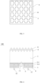
- Step S1 a silicon wafer substrate 1 (i.e., a solar cell substrate) is subjected to a damage removal treatment, a polishing treatment, and a washing treatment sequentially.
- the structure of the silicon wafer substrate 1 is shown in FIG. 1 .
- the silicon wafer substrate 1 is treated with a solution containing KOH at 60°C for damage removal.
- the silicon wafer substrate 1 is polished with a solution containing KOH at 75°C to obtain a polished silicon wafer substrate 1 with 30% of reflectivity.
- the silicon wafer substrate 1 is washed with a mixed solution containing hydrofluoric acid and hydrochloric acid, and deionized water, and then dried.
- the silicon wafer substrate 1 is specifically a p-type silicon substrate. In some other embodiments, the silicon wafer substrate 1 can also be an n-type silicon substrate.
- Step S2 an ultra-thin silicon oxide layer 2-1, a phosphorus-doped amorphous silicon film layer, and a boron-doped silicon oxide layer are successively deposited on a back surface of the silicon wafer substrate 1 through plasma enhanced chemical vapor deposition (PECVD).
- PECVD plasma enhanced chemical vapor deposition
- phosphorane and silane are used as reaction gases, and a flow rate of the phosphorane is lower than a flow rate of the silane. Furthermore, a low flow rate of phosphorane and a high flow rate of silane are introduced at an initial stage of depositing the phosphorus-doped amorphous silicon film layer. After the phosphorus-doped amorphous silicon film layer is deposited to 10 nm to 30 nm, the flow rate of the phosphorane is increased, while the flow rate of the silane remains unchanged during the deposition.
- a small recombination can be formed near the surface of the silicon wafer substrate 1, and a large phosphorus concentration is formed on a side of the phosphorus-doped amorphous silicon film layer away from the silicon wafer substrate 1, which can enhance the field passivation and facilitate the generation of a boron-phosphorus co-doped layer.
- a boron source and silane are used as reaction gases, and a flow rate of the boron source is controlled to be less than 1/3 of a flow rate of the silane.
- Boron phosphorus glass can be formed with phosphorus by boron doping, which provides a relatively strong corrosion resistance.
- the content of boron needs to be controlled at a relatively low level, so that boron elements do not significantly enter a silicon body to cause carrier recombination.
- a thickness of the ultra-thin silicon oxide layer 2-1 is 0.5 nm to 3 nm, preferably 2 nm.
- a thickness of the phosphorus-doped amorphous silicon film layer is 30 nm to 300 nm, preferably 100 nm to 150 nm.
- a thickness of the boron-doped silicon oxide layer is 10 nm to 100 nm, preferably 20 nm to 50 nm.
- the temperature for depositing to form the above ultra-thin silicon oxide layer 2-1, the phosphorus-doped amorphous silicon film and the boron-doped silicon oxide layer is 200°C to 500°C, preferably 450°C.
- Step S3 the silicon wafer substrate 1 is subjected to an annealing treatment.
- the silicon wafer substrate 1 after annealing is shown in FIG. 2 .
- amorphous silicon (i.e., a-Si) deposited by PECVD can be converted into polycrystalline silicon (i.e., Poly-Si) and crystalline grains grow to become larger. Meanwhile, the loose boron-doped silicon oxide layer formed by PECVD can be densified, thereby enhancing the alkali resistance thereof.
- the deposited boron-doped silicon oxide layer absorbs a part of phosphorus elements from the phosphorus-doped polycrystalline silicon film layer 2-2 which is converted from the phosphorus-doped amorphous silicon film layer, and forms a phosphorus-boron co-doped silicon oxide layer 4 with boron atoms, thereby greatly enhancing the corrosion resistance of silicon oxide.
- an annealing temperature is 800°C to 950°C, preferably 850°C to 920°C; and an annealing time is 15 min to 60 min, preferably 45 min.
- Step S4 the back surface of the silicon wafer substrate 1 is patterned to remove a part of the phosphorous-boron co-doped silicon oxide layer 4, thus forming a patterned area 5 not including the phosphorous-boron co-doped silicon oxide layer 4.
- the structure of the back surface of the patterned silicon wafer substrate 1 is shown in FIG. 3 .
- the back surface of the silicon wafer substrate 1 is patterned using a green laser or an ultraviolet laser to remove the phosphorus-boron co-doped silicon oxide layer 4 in a partial area of the back surface of the silicon wafer substrate 1, thereby forming the patterned area 5, such that the p-type area and the n-type area of the solar cell are locally and spatially isolated with each other.
- the patterned area 5 has a width ranging from 300 ⁇ m to 500 ⁇ m.
- the patterned area 5 and the front surface of the silicon wafer substrate 1 are referred to as an area A, which needs to be subjected to a texturing and etching process.
- an area of the back surface of the silicon wafer substrate 1 where the phosphorus-boron co-doped silicon oxide layer 4 is provided is an area B.
- the area B is a surface protected with the phosphorus-boron co-doped silicon oxide layer 4 as a mask, which does not need to be subjected to the texturing and etching process.
- Step S5 the texturing process is performed on the front surface of the silicon wafer substrate 1, and the etching process is performed on the patterned area 5 on the back surface of the silicon wafer substrate 1.
- the textured and etched silicon wafer substrate 1 is shown in FIG. 4 .
- the silicon wafer substrate 1 is treated with a solution containing KOH or NaOH in combination with a texturing additive at a temperature ranged from 70°C to 85°C, so as to texture the front surface of the silicon wafer substrate 1 to form a textured structure, and also to etch the patterned area 5 on the back surface of the silicon wafer substrate 1, for removing the polycrystalline silicon remained in the patterned area 5 and exposing the back surface of the silicon wafer substrate 1 within the patterned area 5.
- a texturing additive at a temperature ranged from 70°C to 85°C, so as to texture the front surface of the silicon wafer substrate 1 to form a textured structure, and also to etch the patterned area 5 on the back surface of the silicon wafer substrate 1, for removing the polycrystalline silicon remained in the patterned area 5 and exposing the back surface of the silicon wafer substrate 1 within the patterned area 5.
- the phosphorus-boron co-doped silicon oxide layer 4 covered on the area B can be removed with a solution containing hydrogen fluoride, after which, the silicon wafer substrate 1 is washed.
- Step S6 a first aluminum oxide film layer 6 and a second aluminum oxide film layer 7 are deposited on the front surface and the back surface of the silicon wafer substrate 1, respectively.
- an atomic layer deposition (ALD) device is used to perform film plating simultaneously on both the front surface and the back surface of the silicon wafer substrate 1 in a single insertion manner, such that a first aluminum oxide film layer 6 is formed on the front surface of the silicon wafer substrate 1, and a second aluminum oxide film layer 7 is formed on the back surface of the silicon wafer substrate 1.
- the first aluminum oxide film layer 6 and the second aluminum oxide film layer 7 both serve the function of passivation.
- the thickness of the first aluminum oxide film layer 6 is 2 nm to 25 nm, and the thickness of the second aluminum oxide film layer 7 is 2 nm to 25 ⁇ m.
- Step S7 a first anti-reflection film layer 8 and a second anti-reflection film layer 9 are deposited on the first aluminum oxide film layer 6 and the second aluminum oxide film layer 7, respectively.
- the first anti-reflection film layer 8 is deposited on the first aluminum oxide film layer 6 on the front surface of the silicon wafer substrate 1 by PECVD
- the second anti-reflection film layer 9 is deposited on the second aluminum oxide film layer 7 on the back surface of the silicon wafer substrate 1 by PECVD.
- the first anti-reflection film layer 8 and the second anti-reflection film layer 9 are each independently any one or a combination thereof selected from silicon nitride, silicon oxynitride, and silicon oxide.
- the first anti-reflection film layer 8 has a thickness from 60 nm to 150 nm
- the second anti-reflection film layer 9 has a thickness from 50 nm to 150 nm.
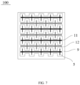
- Step S8 patterned openings are formed in the patterned area 5 of the back surface of the silicon wafer substrate 1 with a laser to form an electrode contact area 10.
- the back surface of the silicon wafer substrate 1 with the patterned openings is shown in FIG. 5 .
- the patterned openings are formed in the patterned area 5 by using a laser according to a predetermined pattern, and the second aluminum oxide film layer 7 and the second anti-reflection film layer 9 within the opening area are removed, thereby forming the electrode contact area 10 of the p-type area.
- the opening area can be in a shape of a dotted line or a dot, and a width of the opening is 30 ⁇ m to 50 ⁇ m.
- Step S9 a first electrode 11 is manufactured in the electrode contact area 10, and a second electrode 12 is manufactured in an area of the back surface of the silicon wafer substrate 1 other than the patterned area 5.
- an electrode paste layer containing a conductive component is printed within the electrode contact area 10 by means of screen printing to form the first electrode 11.
- the first electrode 11 is in contact with the silicon wafer substrate 1.
- a burn-through-type electrode slurry layer containing a conductive component is printed within an area (i.e., an area with a phosphorus-doped polycrystalline silicon layer) of the back surface of the silicon wafer substrate 1 other than the patterned area 5 by means of screen printing to form the second electrode 12.
- the second electrode 12 can be in contact with the phosphorus-doped polycrystalline silicon layer due to the burn-through effect of the electrode slurry.
- a width of the first electrode 11 is 50 ⁇ m to 200 ⁇ m; and a width of the second electrode 12 is 10 ⁇ m to 50 ⁇ m.
- the phosphorus-doped amorphous silicon film layer and the boron-doped silicon oxide layer are deposited on the back surface of the silicon wafer substrate 1, and then the silicon wafer substrate 1 is annealed such that a portion of phosphorus elements in the phosphorus-doped polycrystalline silicon film layer 2-2 are absorbed by the boron-doped silicon oxide layer, and the phosphorus-boron co-doped silicon oxide layer 4 is formed with boron atoms, thereby greatly enhancing the corrosion resistance of silicon oxide.
- the phosphorus-boron co-doped silicon oxide layer 4 is used as a mask layer, which can greatly prolong the time window for processing the subsequent texturing/etching step and can improve the yield of cells.
- An embodiment of the present application provides another method for preparing a back contact solar cell 100.
- This preparation method is basically the same as the preparation method in the embodiments described above, except that the specific methods for forming the phosphorus-boron co-doped silicon oxide layer 4 are different.
- the phosphorus-doped amorphous silicon film layer is first formed on the back surface of the silicon wafer substrate 1, the phosphorus-doped silicon oxide layer is formed on the surface of the phosphorus-doped amorphous silicon film layer away from the silicon wafer substrate 1 through low-pressure chemical vapor deposition (LPCVD), and boron diffusion is performed on the surface of the phosphorus-doped silicon oxide layer to form the phosphorus-boron co-doped silicon oxide layer 4.
- LPCVD low-pressure chemical vapor deposition
- the phosphorus-boron co-doped silicon oxide layer 4 formed in this embodiment also has good corrosion resistance, which can also prolong the time window for the treatment process and can improve the yield of cells.
- the method for preparing the phosphorus-boron co-doped silicon oxide layer 4 is not limited to the above two methods. In addition to the above two methods, any method capable of preparing the phosphorus-boron co-doped silicon oxide layer 4 with good corrosion resistance can be used.
- An embodiment of the present application provides a method of removing a wrap-around layer on a solar cell substrate.
- the solar cell substrate is a silicon substrate 1 with a wrap-around layer on the front surface.
- the area A of the solar cell substrate is the front surface of the solar cell substrate.
- the area B of the solar cell substrate is the back surface of the solar cell substrate.
- a phosphorus-boron co-doped silicon oxide layer 4 is first formed on the area B of the solar cell substrate to serve as a mask layer, and then a wrap-around removal process is performed on the solar cell by using an acid or alkali solution, so as to remove the wrap-around layer on the front surface of the solar cell substrate.
- the phosphorus-boron co-doped silicon oxide layer 4 on the area B can serve as a barrier and provide a prolonged time window for the wrap-around removal process, thereby improving the yield of cells.
- the solar cell substrate is the silicon wafer substrate 1.
- a plated layer is deposited on the back surface of the silicon wafer substrate 1, and the plated layer is wrapped around to the front surface of the silicon wafer substrate 1.
- the back-contact solar cell 100 includes a p-type silicon wafer substrate 1.
- a first aluminum oxide film layer 6 is disposed on the front surface of the silicon wafer substrate 1 (i.e., an upper surface of the silicon wafer substrate 1 in the figure).
- a first anti-reflection film layer 8 is disposed on the first aluminum oxide film layer 6.
- the first aluminum oxide film layer 6 has a thickness ranged from 2 nm to 25 nm.
- the first anti-reflection film layer 8 has a thickness ranged from 60 nm to 150 nm.
- the first anti-reflection film layer 8 is any one or a combination thereof selected from silicon nitride, silicon oxynitride and silicon oxide.
- the back surface (i.e., a lower surface of the silicon wafer substrate 1 in the figure) of the silicon wafer substrate 1 is provided with an n-type doped area, which consists of an ultra-thin silicon oxide layer 2-1 and a phosphorus-doped polycrystalline silicon film layer 2-2 are successively disposed.
- the area of the back surface of the silicon wafer substrate 1 other than the n-type doped area forms the p-type area, in which no ultra-thin silicon oxide layer 2-1 and phosphorus-doped polycrystalline silicon film layer 2-2 is provided, and the n-type doped area and the p-type area are arranged alternately.
- the thickness of the ultra-thin silicon oxide layer 2-1 is 0.5 nm to 3 nm.
- the thickness of the phosphorus-doped polycrystalline silicon film layer 2-2 is 30 nm to 300 nm.
- the width of the n-type doped area is 600 ⁇ m to 1200 ⁇ m.
- the width of the p-type area is 300 ⁇ m to 500 ⁇ m.
- a second aluminum oxide film layer 7 is further provided on the n-type doped area and the p-type area of the back surface of the silicon wafer substrate 1.
- a second anti-reflection film layer 9 is provided on the second aluminum oxide film layer 7.
- the second aluminum oxide film layer 7 has a thickness from 2 ⁇ m to 25 ⁇ m.
- the second anti-reflection film layer 9 has a thickness from 50 nm to 150 nm.
- the second anti-reflection film layer 9 is any one or a combination thereof selected from silicon nitride, silicon oxynitride and silicon oxide.
- a first electrode 11 is provided within the p-type area.
- the first electrode 11 extends through the second aluminum oxide film layer 7 and the second anti-reflection film layer 9 and is in contact with the silicon wafer substrate 1.
- a second electrode 12 is provided within a range corresponding to the n-type doped area of the back surface of the silicon wafer substrate 1.
- the second electrode 12 extends through the second aluminum oxide film layer 7 and the second anti-reflection film layer 9 and is in contact with the phosphorus-doped polycrystalline silicon film layer 2-2.
- the first electrode 11 is an aluminum gate electrode.
- the width of the first electrode 11 is 50 ⁇ m to 200 ⁇ m.
- the second electrode 12 is a silver gate electrode.
- the width of the second electrode 12 is 10 ⁇ m to 50 ⁇ m.
Landscapes
- Photovoltaic Devices (AREA)
Applications Claiming Priority (2)
| Application Number | Priority Date | Filing Date | Title |
|---|---|---|---|
| CN202211199636.4A CN115411150B (zh) | 2022-09-29 | 2022-09-29 | 太阳电池及其制备方法 |
| PCT/CN2023/097010 WO2024066424A1 (zh) | 2022-09-29 | 2023-05-30 | 太阳电池及其制备方法 |
Publications (2)
| Publication Number | Publication Date |
|---|---|
| EP4489082A1 true EP4489082A1 (de) | 2025-01-08 |
| EP4489082A4 EP4489082A4 (de) | 2025-07-30 |
Family
ID=84167827
Family Applications (1)
| Application Number | Title | Priority Date | Filing Date |
|---|---|---|---|
| EP23869677.7A Pending EP4489082A4 (de) | 2022-09-29 | 2023-05-30 | Solarzelle und herstellungsverfahren dafür |
Country Status (5)
| Country | Link |
|---|---|
| US (1) | US20250234671A1 (de) |
| EP (1) | EP4489082A4 (de) |
| CN (1) | CN115411150B (de) |
| AU (1) | AU2023349665B2 (de) |
| WO (1) | WO2024066424A1 (de) |
Families Citing this family (4)
| Publication number | Priority date | Publication date | Assignee | Title |
|---|---|---|---|---|
| CN115411150B (zh) * | 2022-09-29 | 2024-07-09 | 通威太阳能(成都)有限公司 | 太阳电池及其制备方法 |
| CN115832109B (zh) * | 2022-12-22 | 2025-02-07 | 通威太阳能(眉山)有限公司 | 一种太阳电池及其制备方法 |
| CN119604074B (zh) * | 2025-02-08 | 2025-05-02 | 横店集团东磁股份有限公司 | 一种抛光无高度差隔离区tbc电池的制备方法 |
| CN121510710B (zh) * | 2026-01-12 | 2026-04-17 | 安徽晶科能源有限公司 | 一种太阳能电池及其制备方法、叠层电池及光伏组件 |
Family Cites Families (12)
| Publication number | Priority date | Publication date | Assignee | Title |
|---|---|---|---|---|
| KR102657230B1 (ko) * | 2016-11-04 | 2024-04-12 | 오씨아이 주식회사 | 태양 전지 및 이의 제조 방법 |
| CN109244194B (zh) * | 2018-11-06 | 2023-09-01 | 东方日升(常州)新能源有限公司 | 一种低成本p型全背电极晶硅太阳电池的制备方法 |
| CN111354838B (zh) * | 2019-12-27 | 2022-07-15 | 晶澳(扬州)太阳能科技有限公司 | 太阳能电池及其制备方法、n型掺杂硅膜的处理方法 |
| CN113745106B (zh) * | 2021-07-23 | 2025-03-04 | 英利能源(中国)有限公司 | 一种N型TOPCon电池正面绕镀的去除方法 |
| CN113948608B (zh) * | 2021-08-31 | 2024-10-01 | 正泰新能科技股份有限公司 | 一种N-TOPCon电池的绕镀多晶硅去除方法 |
| CN114093755B (zh) * | 2021-11-15 | 2024-05-03 | 长鑫存储技术有限公司 | 半导体结构及其形成方法 |
| CN114497282B (zh) * | 2022-01-27 | 2024-07-23 | 东方日升新能源股份有限公司 | 一种太阳能电池的制备方法及太阳能电池 |
| CN114628547B (zh) * | 2022-03-10 | 2023-07-21 | 泰州中来光电科技有限公司 | 一种背表面局域形貌的太阳电池及其制备方法 |
| CN114823973A (zh) * | 2022-04-20 | 2022-07-29 | 通威太阳能(眉山)有限公司 | 一种p型背接触太阳电池及其制备方法 |
| CN114784142A (zh) * | 2022-04-20 | 2022-07-22 | 通威太阳能(眉山)有限公司 | P型背接触太阳电池及其制备方法 |
| CN114792743B (zh) * | 2022-05-05 | 2024-07-05 | 通威太阳能(成都)有限公司 | 太阳电池及其制备方法、光伏系统 |
| CN115411150B (zh) * | 2022-09-29 | 2024-07-09 | 通威太阳能(成都)有限公司 | 太阳电池及其制备方法 |
-
2022
- 2022-09-29 CN CN202211199636.4A patent/CN115411150B/zh active Active
-
2023
- 2023-05-30 US US18/852,924 patent/US20250234671A1/en active Pending
- 2023-05-30 AU AU2023349665A patent/AU2023349665B2/en active Active
- 2023-05-30 WO PCT/CN2023/097010 patent/WO2024066424A1/zh not_active Ceased
- 2023-05-30 EP EP23869677.7A patent/EP4489082A4/de active Pending
Also Published As
| Publication number | Publication date |
|---|---|
| EP4489082A4 (de) | 2025-07-30 |
| WO2024066424A1 (zh) | 2024-04-04 |
| CN115411150A (zh) | 2022-11-29 |
| AU2023349665B2 (en) | 2026-02-19 |
| CN115411150B (zh) | 2024-07-09 |
| US20250234671A1 (en) | 2025-07-17 |
| AU2023349665A1 (en) | 2024-10-17 |
Similar Documents
| Publication | Publication Date | Title |
|---|---|---|
| EP4489082A1 (de) | Solarzelle und herstellungsverfahren dafür | |
| EP4521473A1 (de) | Solarzelle und herstellungsverfahren dafür sowie fotovoltaisches system | |
| EP4517843A1 (de) | Solarzelle, herstellungsverfahren dafür und anwendung davon | |
| CN101548395B (zh) | 具有改进的表面钝化的晶体硅太阳能电池的制造方法 | |
| US20250351615A1 (en) | Solar cell and preparation method therefor | |
| CN101548392A (zh) | 太阳能电池及其制造方法 | |
| CN113078232A (zh) | 一种n型电池结构及其制备方法 | |
| JP7486654B1 (ja) | 太陽電池 | |
| CN110571304A (zh) | 一种钝化接触双面太阳电池的制作方法 | |
| CN117673207B (zh) | 一种太阳电池的制备方法、太阳电池及光伏组件 | |
| CN113113510A (zh) | 一种p型双面perc太阳电池及其制备方法和应用 | |
| WO2025161787A1 (zh) | 一种太阳电池的制备方法、太阳电池及光伏组件 | |
| CN118367039A (zh) | 太阳能电池和太阳能电池的制造方法 | |
| CN116799095A (zh) | 钝化接触电池及其制备方法 | |
| CN117995944A (zh) | 一种TOPCon电池及其制备方法 | |
| CN114695593A (zh) | 背接触电池的制备方法及背接触电池 | |
| CN116914033B (zh) | 一种双面TOPCon电池的制备方法 | |
| CN118231489A (zh) | 一种p型TOPCon电池及其制备方法 | |
| CN117855333A (zh) | 电池的制备方法及电池的制备系统 | |
| CN210956692U (zh) | Perc电池 | |
| CN120379376A (zh) | 一种tbc电池及其制备方法 | |
| CN120018583A (zh) | TOPCon电池及其制备方法、光伏组件 | |
| CN110120434B (zh) | 电池片及其制备方法 | |
| CN112599618A (zh) | 一种太阳能电池及其制作方法 | |
| CN119384069B (zh) | 一种背接触钝化电池制备方法及结构 |
Legal Events
| Date | Code | Title | Description |
|---|---|---|---|
| STAA | Information on the status of an ep patent application or granted ep patent |
Free format text: STATUS: THE INTERNATIONAL PUBLICATION HAS BEEN MADE |
|
| PUAI | Public reference made under article 153(3) epc to a published international application that has entered the european phase |
Free format text: ORIGINAL CODE: 0009012 |
|
| STAA | Information on the status of an ep patent application or granted ep patent |
Free format text: STATUS: REQUEST FOR EXAMINATION WAS MADE |
|
| 17P | Request for examination filed |
Effective date: 20240930 |
|
| AK | Designated contracting states |
Kind code of ref document: A1 Designated state(s): AL AT BE BG CH CY CZ DE DK EE ES FI FR GB GR HR HU IE IS IT LI LT LU LV MC ME MK MT NL NO PL PT RO RS SE SI SK SM TR |
|
| REG | Reference to a national code |
Ref country code: DE Ref legal event code: R079 Free format text: PREVIOUS MAIN CLASS: H01L0031180000 Ipc: H10F0010165000 |
|
| A4 | Supplementary search report drawn up and despatched |
Effective date: 20250630 |
|
| RIC1 | Information provided on ipc code assigned before grant |
Ipc: H10F 10/165 20250101AFI20250624BHEP Ipc: H10F 71/00 20250101ALI20250624BHEP Ipc: H10F 77/20 20250101ALI20250624BHEP Ipc: H10F 77/70 20250101ALI20250624BHEP |
|
| DAV | Request for validation of the european patent (deleted) | ||
| DAX | Request for extension of the european patent (deleted) |