EP4489300A1 - Symbolbasierte hüllkurvenverfolgung und crestfaktorreduzierung - Google Patents
Symbolbasierte hüllkurvenverfolgung und crestfaktorreduzierung Download PDFInfo
- Publication number
- EP4489300A1 EP4489300A1 EP24185998.2A EP24185998A EP4489300A1 EP 4489300 A1 EP4489300 A1 EP 4489300A1 EP 24185998 A EP24185998 A EP 24185998A EP 4489300 A1 EP4489300 A1 EP 4489300A1
- Authority
- EP
- European Patent Office
- Prior art keywords
- power amplifier
- symbol
- voltage
- crest factor
- envelope tracking
- Prior art date
- Legal status (The legal status is an assumption and is not a legal conclusion. Google has not performed a legal analysis and makes no representation as to the accuracy of the status listed.)
- Pending
Links
- 230000009467 reduction Effects 0.000 title claims abstract description 47
- 239000000969 carrier Substances 0.000 claims description 28
- 239000002131 composite material Substances 0.000 claims description 20
- 238000000034 method Methods 0.000 claims description 20
- 230000007704 transition Effects 0.000 claims description 17
- 238000007667 floating Methods 0.000 claims description 4
- 230000003321 amplification Effects 0.000 claims description 3
- 238000003199 nucleic acid amplification method Methods 0.000 claims description 3
- 230000008901 benefit Effects 0.000 description 15
- 238000004891 communication Methods 0.000 description 10
- 230000007774 longterm Effects 0.000 description 7
- 230000001413 cellular effect Effects 0.000 description 6
- 230000008859 change Effects 0.000 description 6
- JMASRVWKEDWRBT-UHFFFAOYSA-N Gallium nitride Chemical compound [Ga]#N JMASRVWKEDWRBT-UHFFFAOYSA-N 0.000 description 5
- 238000010586 diagram Methods 0.000 description 5
- 238000005265 energy consumption Methods 0.000 description 5
- 238000005516 engineering process Methods 0.000 description 5
- 230000006870 function Effects 0.000 description 5
- 229910002601 GaN Inorganic materials 0.000 description 4
- 238000013528 artificial neural network Methods 0.000 description 4
- 230000005669 field effect Effects 0.000 description 4
- 230000004044 response Effects 0.000 description 4
- 239000003990 capacitor Substances 0.000 description 3
- 238000013459 approach Methods 0.000 description 2
- 230000005540 biological transmission Effects 0.000 description 2
- 238000012937 correction Methods 0.000 description 2
- 125000004122 cyclic group Chemical group 0.000 description 2
- 230000001934 delay Effects 0.000 description 2
- 230000001419 dependent effect Effects 0.000 description 2
- 230000006872 improvement Effects 0.000 description 2
- 230000010363 phase shift Effects 0.000 description 2
- 230000003595 spectral effect Effects 0.000 description 2
- 229910001218 Gallium arsenide Inorganic materials 0.000 description 1
- XUIMIQQOPSSXEZ-UHFFFAOYSA-N Silicon Chemical compound [Si] XUIMIQQOPSSXEZ-UHFFFAOYSA-N 0.000 description 1
- 229910000577 Silicon-germanium Inorganic materials 0.000 description 1
- 230000006978 adaptation Effects 0.000 description 1
- 238000004364 calculation method Methods 0.000 description 1
- 230000010267 cellular communication Effects 0.000 description 1
- 230000000295 complement effect Effects 0.000 description 1
- 230000003111 delayed effect Effects 0.000 description 1
- 238000013461 design Methods 0.000 description 1
- 238000001514 detection method Methods 0.000 description 1
- 230000036541 health Effects 0.000 description 1
- 230000008676 import Effects 0.000 description 1
- 239000012212 insulator Substances 0.000 description 1
- 238000005259 measurement Methods 0.000 description 1
- 229910044991 metal oxide Inorganic materials 0.000 description 1
- 150000004706 metal oxides Chemical class 0.000 description 1
- 238000010295 mobile communication Methods 0.000 description 1
- 238000012986 modification Methods 0.000 description 1
- 230000004048 modification Effects 0.000 description 1
- 238000012806 monitoring device Methods 0.000 description 1
- 230000001537 neural effect Effects 0.000 description 1
- 238000012545 processing Methods 0.000 description 1
- 239000004065 semiconductor Substances 0.000 description 1
- 229910052710 silicon Inorganic materials 0.000 description 1
- 239000010703 silicon Substances 0.000 description 1
- 238000006467 substitution reaction Methods 0.000 description 1
- 238000012360 testing method Methods 0.000 description 1
Images




Classifications
-
- H—ELECTRICITY
- H03—ELECTRONIC CIRCUITRY
- H03F—AMPLIFIERS
- H03F1/00—Details of amplifiers with only discharge tubes, only semiconductor devices or only unspecified devices as amplifying elements
- H03F1/02—Modifications of amplifiers to raise the efficiency, e.g. gliding Class A stages, use of an auxiliary oscillation
- H03F1/0205—Modifications of amplifiers to raise the efficiency, e.g. gliding Class A stages, use of an auxiliary oscillation in transistor amplifiers
- H03F1/0211—Modifications of amplifiers to raise the efficiency, e.g. gliding Class A stages, use of an auxiliary oscillation in transistor amplifiers with control of the supply voltage or current
- H03F1/0216—Continuous control
- H03F1/0222—Continuous control by using a signal derived from the input signal
- H03F1/0227—Continuous control by using a signal derived from the input signal using supply converters
-
- H—ELECTRICITY
- H03—ELECTRONIC CIRCUITRY
- H03F—AMPLIFIERS
- H03F3/00—Amplifiers with only discharge tubes or only semiconductor devices as amplifying elements
- H03F3/20—Power amplifiers, e.g. Class B amplifiers, Class C amplifiers
- H03F3/21—Power amplifiers, e.g. Class B amplifiers, Class C amplifiers with semiconductor devices only
- H03F3/213—Power amplifiers, e.g. Class B amplifiers, Class C amplifiers with semiconductor devices only in integrated circuits
-
- H—ELECTRICITY
- H03—ELECTRONIC CIRCUITRY
- H03F—AMPLIFIERS
- H03F1/00—Details of amplifiers with only discharge tubes, only semiconductor devices or only unspecified devices as amplifying elements
- H03F1/02—Modifications of amplifiers to raise the efficiency, e.g. gliding Class A stages, use of an auxiliary oscillation
- H03F1/0205—Modifications of amplifiers to raise the efficiency, e.g. gliding Class A stages, use of an auxiliary oscillation in transistor amplifiers
- H03F1/0211—Modifications of amplifiers to raise the efficiency, e.g. gliding Class A stages, use of an auxiliary oscillation in transistor amplifiers with control of the supply voltage or current
- H03F1/0244—Stepped control
- H03F1/025—Stepped control by using a signal derived from the input signal
-
- H—ELECTRICITY
- H04—ELECTRIC COMMUNICATION TECHNIQUE
- H04B—TRANSMISSION
- H04B1/00—Details of transmission systems, not covered by a single one of groups H04B3/00 - H04B13/00; Details of transmission systems not characterised by the medium used for transmission
- H04B1/02—Transmitters
- H04B1/04—Circuits
-
- H—ELECTRICITY
- H03—ELECTRONIC CIRCUITRY
- H03F—AMPLIFIERS
- H03F1/00—Details of amplifiers with only discharge tubes, only semiconductor devices or only unspecified devices as amplifying elements
- H03F1/02—Modifications of amplifiers to raise the efficiency, e.g. gliding Class A stages, use of an auxiliary oscillation
- H03F1/0205—Modifications of amplifiers to raise the efficiency, e.g. gliding Class A stages, use of an auxiliary oscillation in transistor amplifiers
- H03F1/0211—Modifications of amplifiers to raise the efficiency, e.g. gliding Class A stages, use of an auxiliary oscillation in transistor amplifiers with control of the supply voltage or current
- H03F1/0216—Continuous control
- H03F1/0233—Continuous control by using a signal derived from the output signal, e.g. bootstrapping the voltage supply
-
- H—ELECTRICITY
- H03—ELECTRONIC CIRCUITRY
- H03F—AMPLIFIERS
- H03F1/00—Details of amplifiers with only discharge tubes, only semiconductor devices or only unspecified devices as amplifying elements
- H03F1/02—Modifications of amplifiers to raise the efficiency, e.g. gliding Class A stages, use of an auxiliary oscillation
- H03F1/0205—Modifications of amplifiers to raise the efficiency, e.g. gliding Class A stages, use of an auxiliary oscillation in transistor amplifiers
- H03F1/0288—Modifications of amplifiers to raise the efficiency, e.g. gliding Class A stages, use of an auxiliary oscillation in transistor amplifiers using a main and one or several auxiliary peaking amplifiers whereby the load is connected to the main amplifier using an impedance inverter, e.g. Doherty amplifiers
-
- H—ELECTRICITY
- H03—ELECTRONIC CIRCUITRY
- H03F—AMPLIFIERS
- H03F1/00—Details of amplifiers with only discharge tubes, only semiconductor devices or only unspecified devices as amplifying elements
- H03F1/32—Modifications of amplifiers to reduce non-linear distortion
- H03F1/3241—Modifications of amplifiers to reduce non-linear distortion using predistortion circuits
-
- H—ELECTRICITY
- H03—ELECTRONIC CIRCUITRY
- H03F—AMPLIFIERS
- H03F3/00—Amplifiers with only discharge tubes or only semiconductor devices as amplifying elements
- H03F3/189—High-frequency amplifiers, e.g. radio frequency amplifiers
- H03F3/19—High-frequency amplifiers, e.g. radio frequency amplifiers with semiconductor devices only
- H03F3/193—High-frequency amplifiers, e.g. radio frequency amplifiers with semiconductor devices only with field-effect devices
-
- H—ELECTRICITY
- H03—ELECTRONIC CIRCUITRY
- H03F—AMPLIFIERS
- H03F3/00—Amplifiers with only discharge tubes or only semiconductor devices as amplifying elements
- H03F3/189—High-frequency amplifiers, e.g. radio frequency amplifiers
- H03F3/19—High-frequency amplifiers, e.g. radio frequency amplifiers with semiconductor devices only
- H03F3/195—High-frequency amplifiers, e.g. radio frequency amplifiers with semiconductor devices only in integrated circuits
-
- H—ELECTRICITY
- H03—ELECTRONIC CIRCUITRY
- H03F—AMPLIFIERS
- H03F3/00—Amplifiers with only discharge tubes or only semiconductor devices as amplifying elements
- H03F3/20—Power amplifiers, e.g. Class B amplifiers, Class C amplifiers
- H03F3/24—Power amplifiers, e.g. Class B amplifiers, Class C amplifiers of transmitter output stages
- H03F3/245—Power amplifiers, e.g. Class B amplifiers, Class C amplifiers of transmitter output stages with semiconductor devices only
-
- H—ELECTRICITY
- H04—ELECTRIC COMMUNICATION TECHNIQUE
- H04L—TRANSMISSION OF DIGITAL INFORMATION, e.g. TELEGRAPHIC COMMUNICATION
- H04L25/00—Baseband systems
- H04L25/02—Details ; arrangements for supplying electrical power along data transmission lines
- H04L25/0264—Arrangements for coupling to transmission lines
- H04L25/0266—Arrangements for providing Galvanic isolation, e.g. by means of magnetic or capacitive coupling
- H04L25/0268—Arrangements for providing Galvanic isolation, e.g. by means of magnetic or capacitive coupling with modulation and subsequent demodulation
-
- H—ELECTRICITY
- H04—ELECTRIC COMMUNICATION TECHNIQUE
- H04L—TRANSMISSION OF DIGITAL INFORMATION, e.g. TELEGRAPHIC COMMUNICATION
- H04L25/00—Baseband systems
- H04L25/02—Details ; arrangements for supplying electrical power along data transmission lines
- H04L25/0264—Arrangements for coupling to transmission lines
- H04L25/028—Arrangements specific to the transmitter end
-
- H—ELECTRICITY
- H03—ELECTRONIC CIRCUITRY
- H03F—AMPLIFIERS
- H03F2200/00—Indexing scheme relating to amplifiers
- H03F2200/102—A non-specified detector of a signal envelope being used in an amplifying circuit
-
- H—ELECTRICITY
- H03—ELECTRONIC CIRCUITRY
- H03F—AMPLIFIERS
- H03F2200/00—Indexing scheme relating to amplifiers
- H03F2200/105—A non-specified detector of the power of a signal being used in an amplifying circuit
-
- H—ELECTRICITY
- H03—ELECTRONIC CIRCUITRY
- H03F—AMPLIFIERS
- H03F2200/00—Indexing scheme relating to amplifiers
- H03F2200/451—Indexing scheme relating to amplifiers the amplifier being a radio frequency amplifier
-
- H—ELECTRICITY
- H03—ELECTRONIC CIRCUITRY
- H03F—AMPLIFIERS
- H03F2201/00—Indexing scheme relating to details of amplifiers with only discharge tubes, only semiconductor devices or only unspecified devices as amplifying elements covered by H03F1/00
- H03F2201/32—Indexing scheme relating to modifications of amplifiers to reduce non-linear distortion
- H03F2201/3227—Adaptive predistortion based on amplitude, envelope or power level feedback from the output of the main amplifier
-
- H—ELECTRICITY
- H04—ELECTRIC COMMUNICATION TECHNIQUE
- H04B—TRANSMISSION
- H04B1/00—Details of transmission systems, not covered by a single one of groups H04B3/00 - H04B13/00; Details of transmission systems not characterised by the medium used for transmission
- H04B1/02—Transmitters
- H04B1/04—Circuits
- H04B2001/0408—Circuits with power amplifiers
-
- H—ELECTRICITY
- H04—ELECTRIC COMMUNICATION TECHNIQUE
- H04B—TRANSMISSION
- H04B1/00—Details of transmission systems, not covered by a single one of groups H04B3/00 - H04B13/00; Details of transmission systems not characterised by the medium used for transmission
- H04B1/02—Transmitters
- H04B1/04—Circuits
- H04B2001/0491—Circuits with frequency synthesizers, frequency converters or modulators
Definitions
- Embodiments of this disclosure relate to systems that generate a bias voltage for a power amplifier with symbol base envelope tracking.
- Radio systems can transmit and receive signals in the form of electromagnetic waves having a frequency in range from approximately 30 kilohertz (kHz) to 300 Gigahertz (GHz). Radio systems can be used for wireless communications, such as cellular communications and/or other wireless network communications.
- kHz kilohertz
- GHz Gigahertz
- Power amplifiers can consume significant power in such systems.
- Power efficient power amplifiers can be desirable for a variety of applications.
- One aspect of this disclosure is a power amplifier system with symbol based envelope tracking that includes a voltage modulator circuit, a power amplifier and a signal path.
- the voltage modulator circuit is configured to generate an output bias voltage that tracks a root mean square symbol power of a radio frequency signal.
- the voltage modulator circuit is configured to adjust the output bias voltage on symbol boundaries.
- the power amplifier is configured to receive the output bias voltage and amplify the radio frequency signal.
- the signal path is configured to provide the radio frequency signal to the power amplifier.
- the signal path includes a crest factor reduction block configured to adjust a crest factor reduction threshold such that the crest factor reduction threshold corresponds to the output bias voltage.
- the power amplifier system can include a quantizer configured to determine a symbol based envelope tracking state based on transmit signal power.
- the voltage modulator circuit can generate the output bias voltage based on the symbol based envelope tracking state.
- the crest factor reduction block can adjust the crest factor reduction threshold based on the symbol based envelope tracking state.
- the signal path can include a digital predistortion system coupled between the crest factor reduction block and a digital-to-analog converter.
- the digital predistortion system can adjust digital predistortion based on the symbol based envelope tracking state.
- the quantizer can receive a composite transmit symbol power associated with a plurality of carriers.
- the signal path can include a digital-to-analog converter coupled between an output of the crest factor reduction block and an input to the power amplifier.
- the power amplifier system can be operable in a discontinuous transmit state.
- a power amplifier transistor of the power amplifier system can have an output terminal connected to ground in the discontinuous transmit state.
- a power amplifier transistor of the power amplifier system can have an output terminal that is floating in the discontinuous transmit state.
- the radio frequency signal can include at least two carriers with different symbol lengths.
- the voltage modulator circuit can adjust the output bias voltage corresponding to symbol boundaries of a carrier of the at least two carriers with a shortest symbol period.
- the power amplifier can include a main power amplifier transistor coupled to the voltage modulator circuit and a peaking power amplifier transistor coupled to a fixed voltage supply.
- the power amplifier can include a main power amplifier transistor coupled to the voltage modulator circuit and a peaking power amplifier transistor coupled to the voltage modulator circuit.
- the power amplifier can include a main power amplifier transistor coupled to the voltage modulator circuit and a peaking power amplifier transistor coupled to a second voltage modulator circuit.
- the voltage modulator circuit can transition the output bias voltage between discrete voltage levels in a time that is in a range between 5 nanoseconds and 200 nanoseconds.
- the voltage modulator circuit can transition the output bias voltage between discrete voltage levels of at least 4 discrete voltage levels on the symbol boundaries.
- a base station can include the power amplifier system.
- Another aspect of this disclosure is a method of radio frequency signal amplification with symbol based envelope tracking.
- the method includes: determining a symbol based envelope tracking state based on transmit signal power; toggling an output bias voltage between a plurality of discrete voltage levels on symbol boundaries of a radio frequency signal based on the symbol based envelope tracking state, wherein the output bias voltage is provided to a power amplifier; adjusting a crest factor reduction threshold of a crest factor reduction block based on the symbol based envelope tracking state, the crest factor reduction block being in a signal path that provides the radio frequency signal to the power amplifier; and amplifying the radio frequency signal with the power amplifier.
- the method can include adjusting digital predistortion in the signal path based on the symbol based envelope tracking state.
- the method can include operating a power amplifier system that includes the power amplifier in a discontinuous transmit state.
- the radio frequency signal can include two carriers having different symbol periods. Toggling the output voltage can occurs on symbol boundaries of a carrier of the two carriers with a shorter symbol period.
- the system includes means for generating an output bias voltage that tracks a root mean square symbol power of a radio frequency signal on a symbol-by-symbol basis, and a signal path configured to provide the radio frequency signal.
- the signal path includes a crest factor reduction block configured to adjust a crest factor reduction threshold such that the crest factor reduction threshold corresponds to the output bias voltage.
- a power amplifier system with symbol based envelope tracking that includes a voltage modulator circuit, a power amplifier, and a signal path configured to provide a radio frequency signal to the power amplifier.
- the voltage modulator circuit is configured to generate an output bias voltage based on a symbol based envelope tracking state such that the output bias voltage tracks a root mean square symbol power of the radio frequency signal on a symbol by symbol basis.
- the power amplifier is configured to receive the output bias voltage and amplify the radio frequency signal.
- The includes a digital predistortion system configured to adjust digital predistortion based on the symbol based envelope tracking state.
- the digital predistortion system can adjust digital predistortion by at least adjusting digital predistortion coefficients.
- the digital predistortion system can adjust digital predistortion by at least adjusting a digital predistortion actuator.
- the power amplifier system can include a quantizer configured to determine the symbol based envelope tracking state based on transmit signal power.
- the quantizer can receive a composite transmit symbol power associated with a plurality of carriers.
- the power amplifier system can include one or more delay blocks coupled between the quantizer and the digital predistortion system.
- the signal path can include a crest factor reduction block configured to adjust a crest factor reduction threshold based on the symbol based envelope tracking state.
- the power amplifier system can be operable in a discontinuous transmit state.
- the radio frequency signal can include at least two carriers with different symbol lengths.
- the voltage modulator circuit can adjust the output bias voltage corresponding to symbol boundaries of a carrier of the at least two carriers with a shortest symbol period.
- the voltage modulator circuit can transition the output bias voltage between discrete voltage levels of at least 4 discrete voltage levels on symbol boundaries.
- the power amplifier can be a Doherty power amplifier.
- Another aspect of this disclosure is a method of radio frequency signal amplification with symbol based envelope tracking.
- the method includes: determining a symbol based envelope tracking state based on transmit signal power; toggling an output bias voltage between a plurality of discrete voltage levels on symbol boundaries of a radio frequency signal based on the symbol based envelope tracking state, wherein the output bias voltage is provided to a power amplifier; adjusting digital predistortion based on the symbol based envelope tracking state, wherein a digital predistortion system that performs the digital predistortion is in a signal path that provides the radio frequency signal to the power amplifier; and amplifying the radio frequency signal with the power amplifier.
- the method can include operating a power amplifier system that includes the power amplifier in a discontinuous transmit state.
- the radio frequency signal can include two carriers having different symbol periods. Toggling the output bias voltage can occur on symbol boundaries of a carrier of the two carriers with a shorter symbol period.
- the system includes a voltage modulator circuit and a signal path configured to provide a radio frequency signal.
- the voltage modulator circuit is configured to generate an output bias voltage based on a symbol based envelope tracking state such that the output bias voltage tracks a root mean square symbol power of the radio frequency signal on a symbol by symbol basis.
- the signal path includes a digital predistortion system configured to adjust digital predistortion based on the symbol based envelope tracking state.
- the system can include a quantizer configured to determine the symbol based envelope tracking state based on an indication of transmit power.
- the system can include one or more delay blocks coupled between the quantizer and the digital predistortion system.
- the quantizer can receive a composite transmit symbol power associated with a plurality of carriers.
- the signal path can include a crest factor reduction block configured to adjust a crest factor reduction threshold based on the symbol based envelope tracking state.
- the voltage modulator circuit can transition the output bias voltage between discrete voltage levels of a plurality of discrete voltage levels in a time that is in a range between 5 nanoseconds and 200 nanoseconds.
- Desirable features of cellular wireless base stations include maximising the data throughput capability, minimising energy consumption, minimising the purchase cost, minimising number of sites, and minimising size and weight.
- the radio frequency (RF) power amplifier (PA) can be the dominant energy consumer in the wireless base station and despite evolutions, such as massive multiple-input multiple output (mMIMO), still remains so. Hence PAs can be a significant part of the base station design when it comes to energy reduction methods.
- RF radio frequency
- mMIMO massive multiple-input multiple output
- the cellular network is also becoming dominated by the newer wireless standards of fourth generation (4G) (Long Term Evolution) and fifth generation (5G) (New Radio) whilst phasing out the older technologies of third generation (3G) (Wideband Code Division Multiple Access) and second generation (2G) (Global System for Mobile communications). It looks as if 3G will phase out first with 2G remaining in a limited number of frequency bands on some continents, e.g. with Europe to support existing machine to machine (M2M) communications infrastructure. Either way, most of the new equipment installed going forward will be purely 4G and 5G using compatible orthogonal frequency-division multiplexing (OFDM) modulation schemes.
- OFDM orthogonal frequency-division multiplexing
- the operating modality of cellular wireless networks is to give the user a good experience. That generally means that if a user suddenly has a demand for network resources, then those network resources are immediately available. In the access network, those network resources include RF power and bandwidth. This generally means the wireless access network is operating with capacity to spare for the vast majority of time.
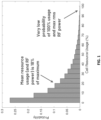
- Figure 1 is a bar graph of probability of cell resource usage taken of a large number of base stations over a number of weeks.
- mean resource usage is 18% of maximum capacity.
- cell resource usage can correspond to root mean square (RMS) RF output power.
- RMS root mean square
- LTE and NR both use OFDM modulation in the RF signal modulation.
- LTE and NR are both symbol based transmission methods.
- N is the numerology 0, 1, 2, ... 4
- the RMS power of the waveform is a constant as it transmits what can be the sum of thousands of sine waves at different frequencies and relative phases. In the next symbol, there is likely a different sum of sine waves, which if there is not much data to transmit may just be a few sine waves.
- Figure 2 is a graph of a radio frequency envelope of a 20 megahertz (MHz) LTE carrier over time with resource usage varying from 100% to 1.6%.
- the y-axis of this graph is the RF envelope (or amplitude).
- the x-axis of this graph is time in 491.52 MHz clock samples.
- the graph includes instantaneous amplitude (peaks) 202, a trace 204 at the RMS level, a trace 206 at the CFR clipping level, and a waveform envelope 208 after clipping at 8 dB peak-to-average power ratio (PAR).
- PAR peak-to-average power ratio
- SBET Symbol Based Envelope Tracking
- Figures 3A, 3B, and 3C are graphs of drain voltage for 5 symbols of a radio frequency signal.
- Figure 3A shows a fixed bias voltage.
- Figure 3B shows a symbol based envelope tracking bias voltage.
- Figure 3C shows a continuous envelope tracking voltage.
- Figures 3A, 3B, and 3C graphically illustrate the concept of envelope tracking.
- the waveform is what a single RF PA transistor is aiming to produce on its output.
- the waveform is symbol based with symbol boundaries at 0, 1, 2, 3, 4, and 5 on the x axis, which corresponds to time.
- the RMS power of the waveform changes on every symbol boundary (where symbols are typically 10s of microseconds long in LTE and NR).
- a fixed drain voltage line 302 is shown in Figure 3A . This the way most cellular wireless base station RF power amplifiers are configured. It is possible that slow changes (seconds or more) of the drain voltage can be achieved to accommodate when the likelihood of high traffic is minimal, such as at night time.
- power amplifier transistor output terminal voltages may only change on symbol boundaries as shown in the Figure 3B .
- the drain voltage can support the maximum peak power within that symbol. This improves PA efficiency as the same RF power is produced in the symbol but operating at a lower drain voltage shown as a symbol based envelope tracking line 304.
- FIG. 3C shows an even higher efficiency mode of operation using full envelope tracking.
- the drain voltage tracks every peak of the waveform envelope in Figure 3C .
- a drain voltage curve 306 tracks each peak on the waveform envelope.
- This efficiency gain can come at the expense of having to change the drain voltage 1000s of times faster than for SBET.
- This full envelope tracking in Figure 3C is an order of magnitude more complex than SBET embodiments disclosed herein and involves sophisticated digital predistortion (DPD) and faster analog switches (e.g., gallium nitride (GaN) switches) than SBET.
- DPD digital predistortion
- GaN gallium nitride
- a full envelope tracking can start skipping troughs to reduce complexity at the cost of losing some efficiency performance.
- the drain voltage only shifts value on the symbol boundaries.
- the drain voltage can have a generally constant voltage level for an entire symbol while the waveform envelope has multiple peaks and troughs for the symbol.
- SBET can switch at the symbol boundaries of the highest numerology carrier in some instances.
- SBET can switch at the symbol boundaries of the lowest numerology carrier in some other instances.
- a power amplifier system can include a voltage modulator circuit to generate an output bias voltage that tracks the RMS symbol power of a radio frequency signal changing on a symbol-by-symbol basis and a power amplifier configured to receive the output bias voltage and amplify the radio frequency signal.
- the power amplifier transmitter system can include a crest factor reduction circuit that adjusts a crest factor reduction threshold on symbol boundaries.
- the power amplifier transmitter system can include a DPD system that accounts for the output bias voltage in DPD.
- a SBET state can be determined based on the RMS power of a transmit signal per symbol.
- the transmit signal can be a composite transmit signal that includes a plurality of carriers in certain application.
- the voltage modulator can adjust the output bias voltage based on the SBET state.
- the crest factor reduction circuit can adjust the crest factor reduction threshold based on the SBET state.
- the DPD system can adjust DPD based on the SBET state.
- the SBET state can transition based on the shortest symbol length. In some other applications where there is a composite transmit signal including two or more carriers with different symbol lengths, the SBET state can transition based on the longest symbol length.
- the power amplifier system can operate in a discontinuous transmit state.
- an output terminal of a power amplifier transistor e.g., a drain of a field effect power amplifier transistor
- ground short circuit
- floating potential open circuit
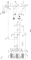
- FIG. 4 is a schematic block diagram of a SBET system 400 according to an embodiment.
- the SBET system 400 is a power amplifier system that includes a power amplifier. As illustrated, the SBET system 400 includes a voltage modulator 402, a supply voltage circuit 404, and a power amplifier 406.
- the SBET system 400 has 4 SBET voltages that can be selected for a drain of a power amplifier transistor and the waveform is made up from 3 individual carriers. Any other suitable number of SBET voltages and/or any other suitable number of individual carriers can be used in some other applications.
- the voltage modulator 402 selects 1 from N fixed voltages from the supply voltage circuit 404 to provide the power amplifier 406. In the illustrated power amplifier 406, the selected voltage is provided to a drain of a power amplifier transistor 407. Each of the voltages from the supply voltage circuit 404 corresponds to an SBET state 1 to N. There can be any suitable number of SBET states for a particular application. For example, in certain applications there are 2 SBET states, 4 SBET states as illustrated in Figure 4 , 8 SBET states, or 16 SBET states.
- the voltage modulator 402 can generate an output bias voltage that tracks an envelope of an RF signal on a symbol-by-symbol basis. The output bias voltage can track the envelope of the radio frequency signal for a group of symbols and/or for each individual symbol.
- the output bias voltage can have a transition time of 10s of nanoseconds.
- the voltage modulator 402 can transition the output bias voltage between discrete voltage levels in a time that is in a range between 5 nanoseconds and 200 nanoseconds.
- the voltage modulator 402 can transition the output bias voltage between discrete voltage levels in a time that is in a range between 5 nanoseconds and 50 nanoseconds.
- the output bias voltage can be stepped significantly (e.g., from 25 Volts (V) to 50 V) on a symbol boundary.
- the SBET system 400 also has a state, which is called discontinuous transmit (DTX) mode, where there is no RF power to transmit in a symbol.
- DTX discontinuous transmit
- the PA output bias voltage can be discharged so it approaches zero volts (e.g., ground) in the DTX state.
- the RF PA 406 is off and should draw negligible power.
- the voltage modulator 402 can provide a constant voltage for an entire symbol and switch state on symbol boundaries.
- the voltage modulator 402 can select from a plurality of discrete voltages (e.g., V1, V2, V3, V4) to provide as the output bias voltage based on SBET state.
- the voltage modulator 402 can toggle the output bias voltage among these discrete voltages on symbol boundaries.
- the voltage modulator 402 can provide a constant voltage for a group of symbols and change state on symbol boundaries.
- the voltage modulator 402 can only switch state on the symbol boundaries of the carrier with the shortest symbol period (highest numerology in NR) when a composite transmit signal includes carriers with different symbol lengths. For instance, in the SBET system 400, if one carrier has a symbol length that is half of the symbol length of the other two carriers, then a quantizer 408 can determine a SBET state at or near symbol boundaries of the symbols having half of the length of the other symbols. The RMS power of the symbols for the other two carriers can hold the same value for two different symbols of the shorter symbol length in this example.
- the voltage modulator 402 can only switch state on the symbol boundaries of a carrier with the longest symbol period (lowest numerology in NR) when a composite transmit signal includes carriers with different symbol lengths. For instance, in the SBET system 400, if a first carrier has a longer symbol length than the second and third carriers, then a quantizer 408 can determine a SBET state at or near symbol boundaries of the symbols of the first carrier of the composite signal. The maximum RMS power of each individual symbol of the second carrier corresponding to one symbol of the first carrier can be used in determining the SBET state. Similarly, the maximum RMS power of each individual symbol of the third carrier corresponding to one symbol of the first carrier can be used in determining the SBET state. The SBET state can thus be determined and set for the peak RMS power of the composite symbol for the length of the longest length symbol in this example.
- the capacitors C RF and C SNUB can be relatively small (e.g., having a capacitance of less than 1 nanofarad) to reduce and/or minimise the switching/settling time of the drain voltage of the power amplifier transistor 407.
- the capacitors Ci to C N (C 1 to C 4 in Figure 4 ) can be larger (e.g., microfarad sized) decoupling capacitors.
- the lowest voltage V N i.e., V 4 in Figure 4
- V N can be limited by the gain reduction caused by lower drain voltage.
- the lowest voltage V N can depend on the PA transistor technology. In certain instances, V N ⁇ 1 ⁇ 2 Vi with an approximate 6 dB gain reduction. With too much gain reduction, the benefit of SBET can start to reduce.
- Each SBET state can have an associated and different CFR threshold level such that each SBET state supports a different RF peak power. In some applications, a subset of SBET states can have different CFR threshold levels to support different RF peak powers.
- the intermediate drain voltage levels can span between the largest and smallest voltages. There is a trade off in choosing the number of discrete voltages, with more discrete voltages generally corresponding to higher efficiency improvement but at the expense of increased cost and board area. A typical range of values for N is from 2 to 4 in certain applications.
- the voltage modulator 402 can implement the DTX state. In the DTX state, all switches of the voltage modulator 402 can be off or one or more switches can be connected to ground.
- the SBET system 400 can include a digital predistortion (DPD) block 412 to compensate for non-linearity of the power amplifier 406.
- the DPD block 412 is a DPD system.
- the DPD block 412 can include a DPD actuator and a DPD adaptation circuit.
- the RF PA non-linearity response can be a function of drain voltage.
- the DPD performed nu the DPD block 412 can also be a function of SBET state.
- SBET state feeds into the DPD block 412 after a matching delay.
- the quantizer 408 can output a SBET state and delay blocks 414 and 416 can add the matching delay so that the SBET state received by the DPD block 412 corresponds to the input signal to the DPD block 412.
- DPD can be adjusted based on the DPD SBET state. Adjusting DPD can involve adjusting DPD coefficients and/or adjusting a DPD actuator. In certain implementations, the DPD model coefficients can be switched on the symbol boundary. Alternatively or additionally, a DPD actuator can be adjusted by enabling and/or disabling certain functionality and/or by adjusting topology of the DPD actuator. This can adjust a DPD model to correspond to an SBET state. The model can be adjusted, for example, by adjusting connections of signal paths in a DPD actuator that include non-linear gain blocks (e.g., lookup tables) and/or by adjusting connections of an artificial neural network in a DPD actuator. Each SBET state or output bias voltage level can have its own DPD model/coefficients, which can switch simultaneously in one clock cycle as the symbol data boundary passes through the DPD block 412.
- the switchover duration can be minimised to 10s of nanoseconds to minimise spectral distortion contribution of switchover on average.
- the distortion may be relatively high in the transition time but on average it can be reduced by approximately 1: 1000, which is the approximate ratio of the voltage transition time to the symbol period.
- An output of the DPD block 412 can be provided to a digital-to-analog converter (DAC) 417 to generate an analog transmit signal.
- DAC digital-to-analog converter
- the analog signal from generated by the DAC 417 can be filtered by a filter 452, amplified by amplifier 453, and split by a hybrid splitter 454.
- the hybrid splitter 454 can provide an RF signal to a main power amplifier transistor 407 and a peaking power amplifier transistor 462 of the power amplifier 406.
- the hybrid splitter 454 can also provide a phase shift such that there is a 90 degree phase shift between the output signals provided by the hybrid splitter 454.
- the power amplifier 406 of the SBET system 400 is a Doherty power amplifier as illustrated.
- EVM impact due to the drain voltage transitions can be less of a concern as the transition occurs during the cyclic prefix period for most symbols. Though it can occur within a symbol in the case of mixed numerology.
- the CFR threshold used to limit the peak power of the digital signal can be a function of the SBET state.
- the SBET state feeds into a CFR block 418 after a matching delay.
- the quantizer 408 can output the SBET state and a delay block 414 can add the matching delay so that the SBET state received by the CFR block 418 corresponds to the input signal to the CFR block 418.
- the CFR block 418 can adjust the CFR threshold based on the SBET state. Accordingly, the CFR threshold can correspond to the output bias voltage provided to the power amplifier 406.
- the CFR block 418 can be implemented by any suitable circuitry. Digital circuitry of a digital signal processor can implement the CFR block 418.
- a transceiver integrated circuit can implement the CFR block 418, for example.
- Adjusting a CFR threshold based on SBET state can be significant to the energy saving performance of SBET system 400.
- a CFR threshold for each SBET state (e.g., drain voltage)
- the peak RF power is defined for each SBET level.
- the lower the CFR threshold the greater the energy saving but the higher the signal distortion and EVM, which in turn should raise the Bit Error Rate (BER).
- BER Bit Error Rate
- a compromise is to ensure that the PAR of any symbol in any SBET state remains greater than or equal to a threshold value.
- An example threshold value is 8 dB.
- Figure 5 is a graph of EVM of each symbol for the 20 MHz LTE carrier corresponding to Figure 2 .
- the EVM for each of the 140 symbols in the waveform of Figure 2 is shown in Figure 5 .
- the RMS EVM of the reduced power symbols is below 1% except for 1 symbol where the CFR clips the most peaks.
- the SBET state is carried by the SBET+DTX bits which are output from the n level quantizer 408.
- the n level quantizer 408 is a 4 level quantizer in Figure 4 because there are 4 SBET voltages provided by the voltage modulator circuit 402.
- the SBET+DTX bits can change state on each symbol boundary. The bits are delayed appropriately so that these bits arrive at the CFR block 418, the DPD block 412, and the voltage modulator 402 and change to their configuration for the new SBET state as the transmit data passes through the SBET system 400 (in the case of the voltage modulator 402 it is the analog signal passing through the field effect transistors of the power amplifier 406).
- the delay blocks 414, 416, and 419 provide such delays for the SBET state bits.
- the appropriate SBET state can be determined by effectively calculating the composite transmit RMS signal power of each complete symbol at an input to the CFR block 418.
- the quantizer 408 can determine the composite transmit RMS signal power.
- the composite transmit signal can be formed from a plurality of carriers.
- each carrier can be received as a frequency domain signal; transformed to the time domain by a respective inverse Fast Fourier Transform (iFFT) block 442A, 442B, 442C; a cyclic prefix (CP) can be added by a respective CP block 444A, 444B, 444C, and upconverted by a respective digital upconverter (DUC) 446A, 446B, 446C.
- Outputs of the DUCs 446A, 446B, 446C can be combined to form the composite transmit signal provided to the CFR block 418.
- calculating transmit power directly at the input of the CFR block 418 may not be ideal as it can take many microseconds at least (and ideally the whole symbol) to get an accurate result. Such a calculation can be ready too late as the composite transmit RMS signal symbol power should be known at the start of the symbol not the end. While 10s of microseconds of delay can be added to the transmit signal path to compute transmit power at the input of the CFR block 418, such a delay is generally not desirable.
- the iFFT gain blocks 432A, 432B, and 432C and multipliers 434A, 434B, and 434C can create a composite transmit signal symbolPwr at the input to the n level quantizer 408 that has a power corresponding to the composite transmit signal at an input of the CFR block 418.
- the iFFT gain blocks 432A, 432B, and 432C can provide gains corresponding to the iFFT blocks 442A, 442B, and 442C.
- the gain applied to in each multiplier 434A, 434B, and 434C can correspond to a gain of a corresponding DUC of the DUCs 446A, 446B, and 446C that form the composite transmit signal that is input to the CFR block 418.
- Processing the frequency domain data rather than time domain data means the symbol power information can be available before the symbol boundary of the compositive transmit signal is provided to the input of the CFR block 418.
- the quantizer 408 can determine an SBET state based on the composite transmit signal symbolPwr it receives.
- the N level quantizer 408 can be preprogramed with N thresholds in a thermometer fashion and output the SBET state as a number from 1 to N.
- the DTX bit is a special condition when the symbol power is zero (or near zero) and can be used disable all switches, so the common switch node of the voltage modulator 402 is open circuit or using an additional switch short the drain of the power transistor407 to ground.
- An aim of adding SBET is to reduce the energy consumption of the RF PAs, which should reduce operating expenses, in wireless base stations. With this reduced energy consumption, performance of the RF PA can be degraded minimally in terms of transmitted signal purity (e.g., EVM) and spectral emissions. It is also desirable to achieve these objectives with minimal increase in equipment cost (capital expenditures).
- EVM transmitted signal purity
- Figures 6A and 6B are graphs of experimental results showing efficiency and power savings using SBET.
- Figure 6A shows the drain efficiency enhancement using SBET with an off-the-shelf GaN Doherty PA Module aimed at small cells and massive MIMO base stations. SBET is compared to using a 31 V fixed voltage supply for these PAs.
- a number of transmit waveforms were generated for a single 20 MHz LTE carrier. The different waveforms were generated so that the number of resource blocks (RB) occupied for data (Physical Downlink Shared Channel (PDSCH)) varied from 1 to 100 RBs.
- RB resource blocks
- PDSCH Physical Downlink Shared Channel
- RS Physical Broadcast Channel
- PCFICH Physical Control Format Indicator Channel
- PDCCH Physical Downlink Control Channel
- the RMS RF output power (averaged over all symbols of a 1 ms frame) varied from 0.9 Watts (W) at 1 RB to 7.5 W at 100 RB, where at 1 RB most of the power is consumed by the non-data physical channels in the waveform.
- W Watts
- RF output power reduces proportionately and initially there is no power saving using SBET until around 60% when the drain voltage has its first drop to a lower voltage. From this point on, SBET provides a significant saving in the direct current (DC) power from the drain supplies.
- DC direct current
- SBET maintains the PA drain efficiency in the 45%-50% range over a relatively wide range of RF output powers.
- the efficiency improvement is largest at the lower powers, but here there is less power to be saved.
- Figure 6B shows that ⁇ 2 W of DC power is saved from around 1% to 60% RB utilization with no power savings above about 70% RB utilization.
- These efficiency figures include the power loss in the modulator, which is relatively small.
- the modulator is ⁇ 99% efficient as a frequency of switch changes is relatively low (low 10s of kHz) and switch losses are mainly from on resistance (Rds) of the switch, which is also relatively low.
- the efficiency enhancements of SBET above turn into energy savings at the base station dependent upon the fraction of time the base station spends at a certain percentage resource usage. If the base station is always at 100% usage, there may be no savings from SBET. If base station usage is always at 1%, the savings can be huge.
- the statistics of base station resource usage in Figure 1 allow us to estimate power saving over an ensemble of base stations in a network averaged over day/night and the week. High resource usage only happens for a small fraction of the time. If we assume a 64 transmit 64 receive (64T64R) massive MIMO base station capable of producing 320 W of RMS power (maximum), that will use about 64 of the PAs corresponding to Figure 6A . The average 320 W capable base station in that network would consume about 9 kWh/day of energy in the output stage of its RF PAs, whereas if SBET was used it would only consume about 6.2 kWh/day of energy. This is a significant energy savings.
- the number of logic lines to drive the voltage modulator 402 is ceiling(log2(n)), where n is the number of voltages (or SBET states). Adding the DTX state could add an extra logic line. Therefore, implementing the DTX state as tri-stating the SBET logic lines can save the need for an extra logic line.
- a tri-state driver can have a third state where it is floating or open circuit for the DTX state.
- a tri-state driver can be implemented in a SBET system with the DTX state.
- a typical CFR block can have 3 consecutive engines that first detect peaks and then correct peaks.
- the CFR block 418 can record the SBET/threshold level with the peak.
- the threshold can then be passed to the correction hardware.
- the correction hardware can reduce the peaks to the desired level.
- There can be a central block that delays the update to each engine so that the threshold changes at the same relative sample for each engine. This can be expanded to non-SBET uses as well, we can now align threshold and the pulse updates to symbol boundaries. Updates can be seamless with these features, where previously one engine was disabled at a time to update thresholds. Such features can be implemented in the CFR block 418 of Figure 4 .
- DPD can measure and then correct a non-linear response of the RF power amplifier.
- the RF PA non-linearity response can be a function of drain voltage. Therefore, a non-linear compensation block in DPD can be a function of SBET state, which means non-linear coefficients/models can change with SBET state and drain voltage at symbol boundaries.
- An additional complication of using certain transistors (e.g., GaN RF transistors) in an RF PA is its charge trapping behavior can alter the PA non-linear characteristics on a long-term timescale of microseconds to milliseconds.
- Neural Predistortion (NPD) can be implemented for long term tracking of the RF PA nonlinearity. Using SBET can amplify the long term dynamic nonlinear behavior compared to a fixed drain voltage, which can be particularly apparent in GaN RF power transistors.
- the PA drain voltage (SBET Level) can be tracked.
- Each of the N SBET levels (e.g., 4 SBET levels of the SBET system 400 of Figure 4 ) can be expanded into a binary level, so there are N binary levels that are passed to a Neural Network (NN).
- NN Neural Network
- Certain NNs use 8-bits MACs. For such NNs, there can be 8-bit programmable values to indicate 0 or 1. This allows the NN to learn the optimal 8-bit values for all the levels.
- Such features can be implemented in the DPD block 412 of Figure 4 .
- the Doherty RF amplifier can be used in wireless infrastructure base stations at RF frequencies below 7 gigahertz (GHz).
- Figures 7A , 7B , and 7C are schematic diagrams of Doherty power amplifiers 406 connected to SBET voltage modulators 402 according to embodiments. These Doherty power amplifiers 406 include a main power amplifier transistor 407 and a peaking power amplifier transistor 462.
- one voltage modulator 402 is used connected to the main power amplifier transistor 407 while the peaking power amplifier transistor 462 has a fixed supply voltage.
- the drain of main power amplifier transistor 407 and the peaking power amplifier transistor 462 are connected to the same voltage modulator 402 at a common node or common switch point. It can be desirable to reduce and/or minimize the physical distance between the output node of the voltage modulator 402 and the power amplifier transistor drains in physical layout.
- SBET can also enhance the efficiency of non-Doherty RF amplifier stages whether used standalone or in other configurations such as a Load Modulated Balanced Amplifier (LMBA).
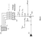
- Figure 8 illustrates an example of voltage modulator 402 with SBET connected to a single power amplifier transistor 802.
- CMOS complementary metal oxide semiconductor
- CMOS complementary metal oxide semiconductor
- a bipolar transistor a bipolar transistor
- a heterojunction bipolar transistor a bipolar power amplifier transistor
- symbol based envelope tracking can modulate a bias voltage at a collector of the bipolar power amplifier transistor and/or any other suitable teachings applied to a drain can be applied to a collector.
- a power amplifier transistor can be implemented by any suitable transistor technology for a particular application.
- Example power amplifier transistors can include, but are not limited to, GaN transistors, silicon transistors, silicon-on-insulator transistors, SiGe transistors, GaAs transistors, SiC transistors, InP transistors, or the like.
- any of the power amplifier transistors disclosed herein can be implemented by two or more power amplifier transistors.
- any suitable principles and advantages disclosed herein can be implemented with radio frequency systems that transmit a radio frequency signal via one or more antennas according to any suitable wireless communication standard.
- a radio frequency system with symbol based envelope tracking in accordance with any suitable principles and advantages disclosed herein can generate signal according to any suitable wireless communication standard, such as a Wi-Fi standard, another local wireless area network standard, a personal wireless area network standard, a future cellular technology standard, or the like.
- apparatuses can include, but are not limited to, communications infrastructure such as wireless or wired communications infrastructure, consumer electronic products, parts of the consumer electronic products, electronic test equipment, vehicular electronic products, industrial electronic products, etc.
- Electronic products can include, but are not limited to, base stations such as cellular base stations, access points, repeaters, relays, wireless communication devices, a mobile phone (for example, a smart phone), a hand-held computer, a tablet computer, a laptop computer, a wearable computing device, a vehicular electronics system, a radio, a wearable health monitoring device, an Internet of Things (IoT) device, etc.
- apparatuses can include unfinished products.
- conditional language used herein such as, among others, “can,” “could,” “might,” “may,” “e.g.,” “for example,” “such as” and the like, unless specifically stated otherwise, or otherwise understood within the context as used, is generally intended to convey that certain embodiments include, while other embodiments do not include, certain features, elements and/or states.
Landscapes
- Engineering & Computer Science (AREA)
- Power Engineering (AREA)
- Physics & Mathematics (AREA)
- Nonlinear Science (AREA)
- Computer Networks & Wireless Communication (AREA)
- Signal Processing (AREA)
- Microelectronics & Electronic Packaging (AREA)
- Amplifiers (AREA)
- Transmitters (AREA)
Applications Claiming Priority (1)
| Application Number | Priority Date | Filing Date | Title |
|---|---|---|---|
| US202363512041P | 2023-07-05 | 2023-07-05 |
Publications (1)
| Publication Number | Publication Date |
|---|---|
| EP4489300A1 true EP4489300A1 (de) | 2025-01-08 |
Family
ID=91782151
Family Applications (1)
| Application Number | Title | Priority Date | Filing Date |
|---|---|---|---|
| EP24185998.2A Pending EP4489300A1 (de) | 2023-07-05 | 2024-07-02 | Symbolbasierte hüllkurvenverfolgung und crestfaktorreduzierung |
Country Status (4)
| Country | Link |
|---|---|
| US (2) | US20250015762A1 (de) |
| EP (1) | EP4489300A1 (de) |
| KR (1) | KR20250007427A (de) |
| CN (1) | CN119276277A (de) |
Families Citing this family (3)
| Publication number | Priority date | Publication date | Assignee | Title |
|---|---|---|---|---|
| US12424989B2 (en) * | 2022-11-29 | 2025-09-23 | Mediatek Inc. | Electronic device and method for envelope tracking |
| EP4637029A1 (de) | 2024-04-18 | 2025-10-22 | Analog Devices, Inc. | Fehlerschutz für symbolbasierte hüllkurvenverfolger |
| EP4637028A1 (de) | 2024-04-18 | 2025-10-22 | Analog Devices, Inc. | Stufenweise aktivierung von schaltern für symbolbasierte hüllkurvenverfolgung |
Citations (5)
| Publication number | Priority date | Publication date | Assignee | Title |
|---|---|---|---|---|
| JP2014003706A (ja) * | 2009-03-02 | 2014-01-09 | Alcatel-Lucent | 電力増幅器によって信号を増幅するための方法、電力増幅器システム、デバイス、コンピュータ・プログラム製品、およびそのデジタル記憶媒体 |
| EP3209071B1 (de) * | 2014-11-20 | 2018-12-19 | ZTE Corporation | Spannungsregelungsverfahren und vorrichtung für leistungsverstärker |
| US20210067386A1 (en) * | 2018-03-30 | 2021-03-04 | Intel IP Corporation | Feedback control systems for wireless devices |
| WO2021042088A2 (en) * | 2020-11-20 | 2021-03-04 | Zeku, Inc. | Switched envelope tracking |
| US20230085587A1 (en) * | 2021-09-14 | 2023-03-16 | Qualcomm Incorporated | Dynamic envelope-tracking supply rail voltage setting |
-
2024
- 2024-06-28 CN CN202410851406.4A patent/CN119276277A/zh active Pending
- 2024-06-28 KR KR1020240085190A patent/KR20250007427A/ko active Pending
- 2024-07-02 EP EP24185998.2A patent/EP4489300A1/de active Pending
- 2024-07-03 US US18/763,905 patent/US20250015762A1/en active Pending
- 2024-07-03 US US18/763,969 patent/US20250015769A1/en active Pending
Patent Citations (5)
| Publication number | Priority date | Publication date | Assignee | Title |
|---|---|---|---|---|
| JP2014003706A (ja) * | 2009-03-02 | 2014-01-09 | Alcatel-Lucent | 電力増幅器によって信号を増幅するための方法、電力増幅器システム、デバイス、コンピュータ・プログラム製品、およびそのデジタル記憶媒体 |
| EP3209071B1 (de) * | 2014-11-20 | 2018-12-19 | ZTE Corporation | Spannungsregelungsverfahren und vorrichtung für leistungsverstärker |
| US20210067386A1 (en) * | 2018-03-30 | 2021-03-04 | Intel IP Corporation | Feedback control systems for wireless devices |
| WO2021042088A2 (en) * | 2020-11-20 | 2021-03-04 | Zeku, Inc. | Switched envelope tracking |
| US20230085587A1 (en) * | 2021-09-14 | 2023-03-16 | Qualcomm Incorporated | Dynamic envelope-tracking supply rail voltage setting |
Also Published As
| Publication number | Publication date |
|---|---|
| KR20250007427A (ko) | 2025-01-14 |
| US20250015762A1 (en) | 2025-01-09 |
| US20250015769A1 (en) | 2025-01-09 |
| CN119276277A (zh) | 2025-01-07 |
Similar Documents
| Publication | Publication Date | Title |
|---|---|---|
| EP4489300A1 (de) | Symbolbasierte hüllkurvenverfolgung und crestfaktorreduzierung | |
| CN113934248B (zh) | 电源调制器 | |
| US10396716B2 (en) | Modulated supply amplifier with adjustable input parameter configuration | |
| US10673384B2 (en) | Power amplifier, radio remote unit, and base station | |
| US8509713B2 (en) | Single envelope tracking system for an active antenna array | |
| Yoo et al. | A watt-level quadrature class-G switched-capacitor power amplifier with linearization techniques | |
| CN105515538A (zh) | 可切换双核功率放大器 | |
| CN111357194B (zh) | 数字功率放大器(dpa)系统和数字多尔蒂功率放大器(ddpa)系统 | |
| US11368175B2 (en) | Radio frequency control circuit | |
| US7274255B2 (en) | Efficient generation of radio frequency currents | |
| JP2016119664A (ja) | 動的電力供給及びデジタルプリディストーションによる効率的なマルチチャネルsatcomのためのシステム及び方法 | |
| US11271600B2 (en) | Transmitters and methods for operating the same | |
| US8145148B2 (en) | Transmitter and communication apparatus | |
| EP2302788A1 (de) | Lastverwaltung für eine verbesserte Hüllkurvennachführungsleistung | |
| Darraji et al. | RF/DSP codesign methodology of enhanced Doherty amplifiers | |
| US20260067138A1 (en) | Transmit signal squelch at symbol boundaries | |
| KR20160095111A (ko) | 제어되는 포락선 추적 변조기 및 적응된 정적 전압을 가진 전력 증폭기 장치 | |
| Becker et al. | Fast-switchable 3.6 GHz GaN Doherty power amplifier for energy-efficient non-continuous transmission of 256-QAM signals | |
| Nesimoglu et al. | The performance and efficiency of envelope elimination and restoration transmitters for future multiple-input multiple-output wireless local area networks | |
| EP2365628A1 (de) | Signalvorverarbeitung für Hüllkurvenmodulatoren | |
| JP6252599B2 (ja) | 送信装置および送信方法 | |
| JP2015050646A (ja) | 送信装置、送信方法及びプログラム | |
| Corse et al. | A method for modeling and analysis of envelope tracking systems |
Legal Events
| Date | Code | Title | Description |
|---|---|---|---|
| PUAI | Public reference made under article 153(3) epc to a published international application that has entered the european phase |
Free format text: ORIGINAL CODE: 0009012 |
|
| STAA | Information on the status of an ep patent application or granted ep patent |
Free format text: STATUS: REQUEST FOR EXAMINATION WAS MADE |
|
| 17P | Request for examination filed |
Effective date: 20240702 |
|
| AK | Designated contracting states |
Kind code of ref document: A1 Designated state(s): AL AT BE BG CH CY CZ DE DK EE ES FI FR GB GR HR HU IE IS IT LI LT LU LV MC ME MK MT NL NO PL PT RO RS SE SI SK SM TR |