EP4490476B1 - Systeme, vorrichtungen und verfahren zur berechnung eines korrekturfaktors zur korrektur einer basislinie eines ramanspektrums durch wellenleiterverstärkte ramanspektroskopietechnologie - Google Patents
Systeme, vorrichtungen und verfahren zur berechnung eines korrekturfaktors zur korrektur einer basislinie eines ramanspektrums durch wellenleiterverstärkte ramanspektroskopietechnologie Download PDFInfo
- Publication number
- EP4490476B1 EP4490476B1 EP23837657.8A EP23837657A EP4490476B1 EP 4490476 B1 EP4490476 B1 EP 4490476B1 EP 23837657 A EP23837657 A EP 23837657A EP 4490476 B1 EP4490476 B1 EP 4490476B1
- Authority
- EP
- European Patent Office
- Prior art keywords
- raman
- raman spectrum
- correction factor
- spectrum
- baseline
- Prior art date
- Legal status (The legal status is an assumption and is not a legal conclusion. Google has not performed a legal analysis and makes no representation as to the accuracy of the status listed.)
- Active
Links
Images
Classifications
-
- G—PHYSICS
- G01—MEASURING; TESTING
- G01J—MEASUREMENT OF INTENSITY, VELOCITY, SPECTRAL CONTENT, POLARISATION, PHASE OR PULSE CHARACTERISTICS OF INFRARED, VISIBLE OR ULTRAVIOLET LIGHT; COLORIMETRY; RADIATION PYROMETRY
- G01J3/00—Spectrometry; Spectrophotometry; Monochromators; Measuring colours
- G01J3/28—Investigating the spectrum
-
- G—PHYSICS
- G01—MEASURING; TESTING
- G01J—MEASUREMENT OF INTENSITY, VELOCITY, SPECTRAL CONTENT, POLARISATION, PHASE OR PULSE CHARACTERISTICS OF INFRARED, VISIBLE OR ULTRAVIOLET LIGHT; COLORIMETRY; RADIATION PYROMETRY
- G01J3/00—Spectrometry; Spectrophotometry; Monochromators; Measuring colours
- G01J3/28—Investigating the spectrum
- G01J3/44—Raman spectrometry; Scattering spectrometry ; Fluorescence spectrometry
-
- G—PHYSICS
- G01—MEASURING; TESTING
- G01J—MEASUREMENT OF INTENSITY, VELOCITY, SPECTRAL CONTENT, POLARISATION, PHASE OR PULSE CHARACTERISTICS OF INFRARED, VISIBLE OR ULTRAVIOLET LIGHT; COLORIMETRY; RADIATION PYROMETRY
- G01J3/00—Spectrometry; Spectrophotometry; Monochromators; Measuring colours
- G01J3/02—Details
- G01J3/0205—Optical elements not provided otherwise, e.g. optical manifolds, diffusers, windows
- G01J3/0218—Optical elements not provided otherwise, e.g. optical manifolds, diffusers, windows using optical fibers
-
- G—PHYSICS
- G01—MEASURING; TESTING
- G01N—INVESTIGATING OR ANALYSING MATERIALS BY DETERMINING THEIR CHEMICAL OR PHYSICAL PROPERTIES
- G01N21/00—Investigating or analysing materials by the use of optical means, i.e. using sub-millimetre waves, infrared, visible or ultraviolet light
- G01N21/17—Systems in which incident light is modified in accordance with the properties of the material investigated
- G01N21/25—Colour; Spectral properties, i.e. comparison of effect of material on the light at two or more different wavelengths or wavelength bands
- G01N21/27—Colour; Spectral properties, i.e. comparison of effect of material on the light at two or more different wavelengths or wavelength bands using photo-electric detection ; circuits for computing concentration
- G01N21/274—Calibration, base line adjustment, drift correction
-
- G—PHYSICS
- G01—MEASURING; TESTING
- G01N—INVESTIGATING OR ANALYSING MATERIALS BY DETERMINING THEIR CHEMICAL OR PHYSICAL PROPERTIES
- G01N21/00—Investigating or analysing materials by the use of optical means, i.e. using sub-millimetre waves, infrared, visible or ultraviolet light
- G01N21/62—Systems in which the material investigated is excited whereby it emits light or causes a change in wavelength of the incident light
- G01N21/63—Systems in which the material investigated is excited whereby it emits light or causes a change in wavelength of the incident light optically excited
- G01N21/65—Raman scattering
-
- G—PHYSICS
- G01—MEASURING; TESTING
- G01J—MEASUREMENT OF INTENSITY, VELOCITY, SPECTRAL CONTENT, POLARISATION, PHASE OR PULSE CHARACTERISTICS OF INFRARED, VISIBLE OR ULTRAVIOLET LIGHT; COLORIMETRY; RADIATION PYROMETRY
- G01J3/00—Spectrometry; Spectrophotometry; Monochromators; Measuring colours
- G01J3/28—Investigating the spectrum
- G01J2003/2866—Markers; Calibrating of scan
-
- G—PHYSICS
- G01—MEASURING; TESTING
- G01N—INVESTIGATING OR ANALYSING MATERIALS BY DETERMINING THEIR CHEMICAL OR PHYSICAL PROPERTIES
- G01N2201/00—Features of devices classified in G01N21/00
- G01N2201/08—Optical fibres; light guides
Definitions
- the invention relates to the field of Raman signal processing.
- it relates to a system, an integrated semiconductor device and a method for calculating a correction factor for correcting the baseline of a Raman spectrum generated by a waveguide-amplified Raman spectroscopy technology.
- baseline also called “background noise” in French or “baseline” in English.
- the baseline is considered to be due either to Rayleigh scattering or to the fluorescence of certain organic molecules (i.e., the emission of light at a certain wavelength by a substance irradiated at another wavelength) which comes from the samples analyzed.
- the material of the waveguide, in which the optical wave propagates also produces a Raman effect and thus contributes to the formation of the baseline.
- the invention aims to solve, at least partially, this need.
- a first aspect of the invention relates to a system for calculating a correction factor for correcting a baseline of a Raman spectrum acquired by at least one waveguide-amplified Raman spectroscopy device, called a Raman sensor on chip, as defined in claim 1.
- the on-chip Raman sensor is designed to implement a waveguide-amplified Raman spectroscopy technology and which, in response to the irradiation of at least one excitation radiation on a continuous fluid medium to be studied, called the analyte medium, having at least a first refractive index, is configured to acquire a first optical spectrum, called the first Raman spectrum, which comprises a plurality of discrete wavelengths and which is representative of the analyte medium.
- system also includes at least one memory and at least one processor.
- the on-chip Raman sensor includes a substrate that defines at least one surface, and at least one optical waveguide, which is formed from an optically transmissive material, which is disposed in whole or in part on or within the substrate, and which is configured to guide at least one light beam at at least one working wavelength.
- the memory is configured to store a database each record of which is configured to associate a correction factor with an analyte medium, a predetermined reference medium, a working wavelength, a first refractive index of the analyte medium and a second refractive index of the predetermined reference medium.
- the memory is also configured to store processor-executable instructions.
- the processor-executable instructions implement, first of all, a first calculation step, for each wavelength of the first Raman spectrum, of a first parameter, called the first Raman conversion efficiency parameter, which describes the Raman conversion efficiency of the on-chip Raman sensor in the predetermined reference medium.
- the processor-executable instructions implement a second step of calculating, for each wavelength of the first Raman spectrum, a second parameter, called the second Raman conversion efficiency parameter, which describes the Raman conversion efficiency of the on-chip Raman sensor in the analyte medium.
- the processor-executable instructions implement a third step of calculating, for each wavelength of the first Raman spectrum, a correction factor that corresponds to a ratio between the first Raman conversion efficiency parameter and the second Raman conversion efficiency parameter, the correction factor being designed to correct the baseline of the second Raman spectrum.
- each correction factor is designed to correct the baseline of a second optical spectrum, called the second Raman spectrum, the baseline being caused by the on-chip Raman sensor, when generating the second Raman spectrum, in response to the irradiation of at least one excitation radiation on a predetermined reference medium which has at least one second refractive index different from the first refractive index, the second Raman spectrum comprising a plurality of discrete wavelengths and being representative of the predetermined reference medium.
- each correction factor corresponds, for each wavelength of the first Raman spectrum, to a ratio between the first Raman conversion efficiency parameter and the second Raman conversion efficiency parameter.
- the processor-executable instructions further implement a step of correcting the baseline of the second Raman spectrum from the correction factor, so as to obtain a second corrected Raman spectrum which is representative of the baseline of the first Raman spectrum, the baseline being caused by the on-chip Raman sensor during acquisition of the first Raman spectrum.
- processor-executable instructions also implement a step of subtracting the second corrected Raman spectrum from the first Raman spectrum.
- a second aspect of the invention relates to an integrated semiconductor device for calculating a correction factor for correcting a baseline of a Raman spectrum acquired by the integrated semiconductor device, as defined in claim 3.
- the integrated semiconductor device is designed to implement a waveguide-amplified Raman spectroscopy technology, and is configured to, in response to the irradiation of at least one excitation radiation on a continuous fluid medium to be studied, called the analyte medium, having at least a first refractive index, acquire a first optical spectrum, called the first Raman spectrum, which comprises a plurality of discrete wavelengths and which is representative of the analyte medium.
- the integrated semiconductor device includes a substrate that defines at least one surface, and at least one optical waveguide which is formed in an optical transmission material, which is disposed in whole or in part on or in the substrate, and which is configured to guide at least one light beam at at least one working wavelength.
- the integrated semiconductor device also comprises at least one processor and at least one memory which is configured to store a database each record of which is configured to associate a correction factor with an analyte medium, a predetermined reference medium, a working wavelength, a first refractive index of the analyte medium and a second refractive index of the predetermined reference medium.
- the memory is also configured to store processor-executable instructions.
- the processor-executable instructions implement, first of all, a first step of calculating, for each wavelength of the first Raman spectrum, a first parameter, called the first Raman conversion efficiency parameter, which describes the Raman conversion efficiency of the semiconductor device integrated in the predetermined reference medium.
- the processor-executable instructions implement a second step of calculating, for each wavelength of the first Raman spectrum, a second parameter, called the second Raman conversion efficiency parameter, which describes the Raman conversion efficiency of the semiconductor device integrated in the analyte medium.
- the processor-executable instructions implement a third step of calculating, for each wavelength of the first Raman spectrum, a correction factor that corresponds to a ratio between the first Raman conversion efficiency parameter and the second Raman conversion efficiency parameter, the correction factor being designed to correct the baseline of the second Raman spectrum.
- each correction factor is designed to correct the baseline of a second optical spectrum, called the second Raman spectrum, which is caused by the integrated semiconductor device, when generating the second Raman spectrum, in response to the irradiation of at least one excitation radiation on a predetermined reference medium which has at least one second refractive index different from the first refractive index, the second Raman spectrum comprising a plurality of discrete wavelengths and being representative of the predetermined reference medium.
- each correction factor corresponds, for each wavelength of the first Raman spectrum, to a ratio between the first Raman conversion efficiency parameter and the second Raman conversion efficiency parameter.
- the processor-executable instructions are configured to:
- the processor-executable instructions further implement a step of correcting the baseline of the second Raman spectrum from the correction factor, so as to obtain a second corrected Raman spectrum which is representative of the baseline of the first Raman spectrum, the baseline being caused by the integrated semiconductor device during the acquisition of the first Raman spectrum.
- processor-executable instructions also implement a step of subtracting the second corrected Raman spectrum from the first Raman spectrum.
- a third aspect of the invention relates to a computer-implemented method of calculating a correction factor for correcting a baseline of a Raman spectrum acquired by at least one waveguide-amplified Raman spectroscopy device, called an on-chip Raman sensor, method as defined in claim 5.
- the on-chip Raman sensor which is designed to implement a waveguide-amplified Raman spectroscopy technology and which, in response to the irradiation of at least one excitation radiation on a continuous fluid medium to be studied, called the analyte medium, having at least a first refractive index, is configured to acquire a first optical spectrum, called the first Raman spectrum, which comprises a plurality of discrete wavelengths and which is representative of the analyte medium.
- the on-chip Raman sensor comprises a substrate that defines at least one surface, and at least one optical waveguide that is formed from an optically transmissive material, that is disposed in whole or in part on or in the substrate, and that is configured to guide at least one light beam at at least one working wavelength.
- the method comprises a step of acquiring a second optical spectrum, called second Raman spectrum, by the on-chip Raman sensor, in response to the irradiation of at least one excitation radiation on a predetermined reference medium which has at least one second refractive index different from the first refractive index, the second Raman spectrum comprising a plurality of wavelengths discrete waveforms and being representative of the predetermined reference medium, the second Raman spectrum generation causing the formation of a baseline of the second Raman spectrum.
- a second optical spectrum called second Raman spectrum
- the method also comprises a first step of calculation, by a processor, for each wavelength of the first Raman spectrum, of a first parameter, called first Raman conversion efficiency parameter, which describes the Raman conversion efficiency of the on-chip Raman sensor in the predetermined reference medium.
- first Raman conversion efficiency parameter which describes the Raman conversion efficiency of the on-chip Raman sensor in the predetermined reference medium.
- the method also comprises a second step of calculation, by a processor, for each wavelength of the first Raman spectrum, of a second parameter, called second Raman conversion efficiency parameter, which describes the Raman conversion efficiency of the on-chip Raman sensor in the analyte medium.
- second Raman conversion efficiency parameter which describes the Raman conversion efficiency of the on-chip Raman sensor in the analyte medium.
- the method also comprises a third step of calculating, by a processor, for each wavelength of the first Raman spectrum, a correction factor which corresponds to a ratio between the first Raman conversion efficiency parameter and the second Raman conversion efficiency parameter.
- the first calculation step and the second calculation step are carried out from an optical simulation of at least one optical mode of the optical waveguide of the on-chip Raman sensor.
- the third calculation step comprises dividing the first Raman conversion efficiency parameter by the second Raman conversion efficiency parameter.
- the method further comprises a step of storing, by a processor, the correction factor in a database each record of which is configured to associate a correction factor with an analyte medium, a predetermined reference medium, a working wavelength, a first refractive index of the analyte medium and a second refractive index of the predetermined reference medium.
- the predetermined reference medium is a continuous fluid medium.
- the predetermined reference medium is a continuous solid medium.
- the method also comprises a step of subtracting, by a processor, the second corrected Raman spectrum from the second Raman spectrum.
- the step of correcting the baseline of the second Raman spectrum comprises multiplying the second Raman spectrum with the correction factor associated with a wavelength of the first Raman spectrum.
- the method further comprises a step of selecting, by a processor, the correction factor from a database as a function of, at least, the analyte medium, the predetermined reference medium, the first refractive index of the analyte medium, the second refractive index of the predetermined reference medium and the working wavelength.
- WERS waveguide-enhanced Raman spectroscopy
- Raman spectroscopy probes are generally used in the fields of biochemical detection, research or biochemical production.
- Raman spectroscopy involves illuminating a material to be analyzed in such a way as to make the molecular bonds that compose it vibrate. These vibrations are materialized by a secondary photon emission whose wavelength shift relative to the excitation wave, known as the Raman effect, represents a characteristic signature of each bond, called the Raman spectrum.
- each vibrational frequency is specific to the chemical bond and symmetry of a molecule so that the intensity peaks of a Raman spectrum reveal qualitative and quantitative information about the nature of the vibrational molecular dynamics of a sample (e.g., frequency, symmetry of vibrations).
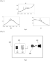
- FIG. 1 illustrates three examples of Raman spectra, (a), (b) and (c).
- the abscissa of its spectra indicates the Raman shift which corresponds to the jump energies between the fundamental vibration levels and which is expressed cm -1 (wave number which recalls the direct proportionality between the energy and the inverse of the wavelength of electromagnetic radiation).
- the ordinate of these spectra corresponds to the scattered Raman intensity for each wave number.
- spectra (a), (b) and (c) each include a baseline which is illustrated in dotted lines.
- a monochromatic laser-type light signal is guided into a waveguide.
- the evanescent field of the guided light i.e., the part of the light that is physically present outside the waveguide
- these molecules will emit Raman radiation.
- a part of this Raman radiation is collected in the waveguide, which then constitutes a Raman signal of interest.
- the waveguide material in which the light signal propagates, also produces a Raman effect and thus contributes to the formation of the baseline.
- the baseline is eliminated from a Raman spectrum by using a reference measurement which is subtracted from the real measurement.
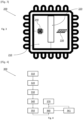
- the system 100 may include two or more first on-chip Raman sensors 110, two or more memories 120, and/or two or more processors 130.
Landscapes
- Physics & Mathematics (AREA)
- Spectroscopy & Molecular Physics (AREA)
- General Physics & Mathematics (AREA)
- Health & Medical Sciences (AREA)
- Chemical & Material Sciences (AREA)
- Analytical Chemistry (AREA)
- Biochemistry (AREA)
- General Health & Medical Sciences (AREA)
- Life Sciences & Earth Sciences (AREA)
- Immunology (AREA)
- Pathology (AREA)
- Engineering & Computer Science (AREA)
- Mathematical Physics (AREA)
- Theoretical Computer Science (AREA)
- Nuclear Medicine, Radiotherapy & Molecular Imaging (AREA)
- Investigating, Analyzing Materials By Fluorescence Or Luminescence (AREA)
Claims (12)
- System (100) zur Berechnung eines Korrekturfaktors zur Korrektur einer Basislinie eines Raman-Spektrums, das von mindestens einer Raman-Spektroskopievorrichtung mit Wellenleiterverstärkung, bezeichnet als On-Chip-Raman-Sensor (110), erfasst wurde, wobei das System (100) umfasst:- den On-Chip-Raman-Sensor (110), der ausgelegt ist, um eine wellenleiterverstärkte Raman-Spektroskopie-Technologie umzusetzen, und der als Reaktion auf die Bestrahlung mindestens einer Anregungsstrahlung auf ein zu untersuchendes kontinuierliches fluides Medium, bezeichnet als Analytmedium, das mindestens einen ersten Brechungsindex aufweist, ausgelegt ist, um ein erstes optisches Spektrum, bezeichnet als erstes Raman-Spektrum, zu erfassen, das eine Vielzahl diskreter Wellenlängen umfasst und für das Analytmedium repräsentativ ist, und- mindestens einen Speicher (120), und- mindestens einen Prozessor (130),
wobei- der On-Chip-Raman-Sensor (110) umfasst,- ein Substrat, das mindestens eine Oberfläche definiert, und- mindestens einen optischen Wellenleiter, der aus einem optisch durchlässigen Material besteht, der ganz oder teilweise auf oder in dem Substrat angeordnet ist und der ausgelegt ist, um mindestens einen Lichtstrahl mit mindestens einer Arbeitswellenlänge zu führen,- der Speicher (120) ausgelegt ist, um zu speichern,- eine Datenbank (121), deren jede Eintragung ausgelegt ist, um einen Korrekturfaktor einem Analytmedium, einem vorbestimmten Referenzmedium, einer Arbeitswellenlänge, einem ersten Brechungsindex des Analytmediums und einem zweiten Brechungsindex des vorbestimmten Referenzmediums zuzuordnen,- prozessorausführbare Anweisungen (122), die implementieren,- einen ersten Berechnungsschritt für jede Wellenlänge des ersten Raman-Spektrums eines ersten Parameters, bezeichnet als erster Raman-Umwandlungswirkungsgrad-Parameter, der den Raman-Umwandlungswirkungsgrad des On-Chip-Raman-Sensors (110) in dem vorbestimmten Referenzmedium beschreibt,- einen zweiten Berechnungsschritt für jede Wellenlänge des ersten Raman-Spektrums eines zweiten Parameters, bezeichnet als zweiter Raman-Umwandlungswirkungsgrad-Parameter, der den Raman-Umwandlungswirkungsgrad des On-Chip-Raman-Sensors (110) im Analytmedium beschreibt, und- einen dritten Berechnungsschritt für jede Wellenlänge des ersten Raman-Spektrums eines Korrekturfaktors, der einem Verhältnis zwischen dem ersten Raman-Umwandlungswirkungsgrad-Parameter und dem zweiten Raman-Umwandlungswirkungsgrad-Parameter entspricht, wobei der Korrekturfaktor ausgelegt ist, um die Basislinie des zweiten Raman-Spektrums zu korrigieren,
wobei jeder Korrekturfaktor- ausgelegt ist, um die Basislinie eines zweiten optischen Spektrums, bezeichnet als zweites Raman-Spektrum, zu korrigieren, wobei die Basislinie durch den On-Chip-Raman-Sensor (110) bei der Erzeugung des zweiten Raman-Spektrums als Reaktion auf die Bestrahlung mindestens einer Anregungsstrahlung auf ein vorbestimmtes Referenzmedium bewirkt wird, das mindestens einen zweiten Brechungsindex aufweist, der sich vom ersten Brechungsindex unterscheidet, wobei das zweite Raman-Spektrum eine Vielzahl diskreter Wellenlängen umfasst und für das vorbestimmte Referenzmedium repräsentativ ist,- für jede Wellenlänge des ersten Raman-Spektrums einem Verhältnis zwischen einem ersten Raman-Umwandlungswirkungsgrad-Parameter und dem zweiten Raman-Umwandlungswirkungsgrad-Parameter entspricht,- wobei der Prozessor (130) ausgelegt ist, um die ausführbaren Anweisungen (122) auszuführen. - System (100) zur Berechnung eines Korrekturfaktors nach Anspruch 1, wobei die prozessorausführbaren Anweisungen (122) ferner implementieren,- einen Korrekturschritt der Basislinie des zweiten Raman-Spektrums anhand des Korrekturfaktors, um ein korrigiertes zweites Raman-Spektrum zu erhalten, das für die Basislinie des ersten Raman-Spektrums repräsentativ ist, wobei die Basislinie durch den On-Chip-Raman-Sensor (110) bei der Erfassung des ersten Raman-Spektrums bewirkt wird, und- einen Subtraktionsschritt des korrigierten zweiten Raman-Spektrums vom ersten Raman-Spektrum.
- System (100) zur Berechnung eines Korrekturfaktors nach einem der Ansprüche 1 bis 2, wobei das System in Form einer integrierten Halbleitervorrichtung (200) ausgeführt ist, umfassend,- den On-Chip-Raman-Sensor (110), der in die integrierte Halbleitervorrichtung (200) integriert ist,- den Speicher (120), der in Form eines integrierten Speichers (230) ausgeführt ist, und- den Prozessor (130), der in Form eines integrierten Prozessors (240) ausgeführt ist.
- Verfahren, das von einem Rechner umgesetzt wird, zum Berechnen (300) eines Korrekturfaktors zum Korrigieren einer Basislinie eines Raman-Spektrums, das von mindestens einer Raman-Spektroskopievorrichtung mit Wellenleiterverstärkung, bezeichnet als On-Chip-Raman-Sensor (110), erfasst wird, wobei der On-Chip-Raman-Sensor (110) ausgelegt ist, um eine wellenleiterverstärkte Raman-Spektroskopie-Technologie umzusetzen, und der als Reaktion auf die Bestrahlung mindestens einer Anregungsstrahlung auf ein zu untersuchendes kontinuierliches fluides Medium, bezeichnet als Analytmedium, das mindestens einen ersten Brechungsindex aufweist, ausgelegt ist, um ein erstes optisches Spektrum, bezeichnet als erstes Raman-Spektrum, zu erfassen, das eine Vielzahl diskreter Wellenlängen umfasst und das für das Analytmedium repräsentativ ist, wobei der On-Chip-Raman-Sensor (110) umfasst,- ein Substrat, das mindestens eine Oberfläche definiert, und- mindestens einen optischen Wellenleiter, der aus einem optisch durchlässigen Material besteht, der ganz oder teilweise auf oder in dem Substrat angeordnet ist und der ausgelegt ist, um mindestens einen Lichtstrahl mit mindestens einer Arbeitswellenlänge zu führen,wobei das Verfahren (300) umfasst,- einen Schritt der Erfassung (310) eines zweiten optischen Spektrums, bezeichnet als zweites Raman-Spektrum, durch den On-Chip-Raman-Sensor (110) als Reaktion auf die Bestrahlung mindestens einer Anregungsstrahlung auf ein vorbestimmtes Referenzmedium, das mindestens einen zweiten Brechungsindex aufweist, der sich vom ersten Brechungsindex unterscheidet, wobei das zweite Raman-Spektrum eine Vielzahl diskreter Wellenlängen umfasst und für das vorbestimmte Referenzmedium repräsentativ ist, wobei die Erzeugung des zweiten Raman-Spektrums die Bildung einer Basislinie des zweiten Raman-Spektrums bewirkt,- einen ersten Berechnungsschritt (320) durch einen Prozessor für jede Wellenlänge des ersten Raman-Spektrums eines ersten Parameters, bezeichnet als erster Raman-Umwandlungswirkungsgrad-Parameter, der den Raman-Umwandlungswirkungsgrad des On-Chip-Raman-Sensors (110) im vorbestimmten Referenzmedium beschreibt,- einen zweiten Berechnungsschritt (330) durch einen Prozessor für jede Wellenlänge des ersten Raman-Spektrums eines zweiten Parameters, bezeichnet als zweiter Raman-Umwandlungswirkungsgrad-Parameter, der den Raman-Umwandlungswirkungsgrad des On-Chip-Raman-Sensors (110) im Analytmedium beschreibt, und- einen dritten Berechnungsschritt (340) durch einen Prozessor für jede Wellenlänge des ersten Raman-Spektrums eines Korrekturfaktors, der einem Verhältnis zwischen dem ersten Raman-Umwandlungswirkungsgrad-Parameter und dem zweiten Raman-Umwandlungswirkungsgrad-Parameter entspricht, wobei der Korrekturfaktor ausgelegt ist, um die Basislinie des zweiten Raman-Spektrums zu korrigieren.
- Verfahren, das von einem Rechner umgesetzt wird, zum Berechnen (300) eines Korrekturfaktors nach Anspruch 4, wobei der erste Berechnungsschritt (320) und der zweite Berechnungsschritt (330) ausgehend von einer optischen Simulation mindestens eines optischen Modus des optischen Wellenleiters des On-Chip-Raman-Sensors (110) durchgeführt werden.
- Verfahren, das von einem Rechner umgesetzt wird, zum Berechnen (300) eines Korrekturfaktors nach einem der Ansprüche 4 und 5, wobei der dritte Berechnungsschritt (340) eine Division des ersten Raman-Umwandlungswirkungsgrad-Parameters durch den zweiten Raman-Umwandlungswirkungsgrad-Parameter umfasst.
- Verfahren, das von einem Rechner umgesetzt wird, zum Berechnen (300) eines Korrekturfaktors nach einem der Ansprüche 4 bis 6, das ferner einen Schritt des Speicherns (350) durch einen Prozessor des Korrekturfaktors in einer Datenbank (121) umfasst, deren jede Eintragung ausgelegt ist, um einen Korrekturfaktor einem Analytmedium, einem vorbestimmten Referenzmedium, einer Arbeitswellenlänge, einem ersten Brechungsindex des Analytmediums und einem zweiten Brechungsindex des vorbestimmten Referenzmediums zuzuordnen.
- Verfahren, das von einem Rechner umgesetzt wird, zum Berechnen (300) eines Korrekturfaktors nach einem der Ansprüche 4 bis 7, wobei das vorbestimmte Referenzmedium ein kontinuierliches fluides Medium ist.
- Verfahren, das von einem Rechner umgesetzt wird, zum Berechnen (300) eines Korrekturfaktors nach einem der Ansprüche 4 bis 7, wobei das vorbestimmte Referenzmedium ein kontinuierliches festes Medium ist.
- Verfahren, das von einem Rechner umgesetzt wird, zum Berechnen (300) eines Korrekturfaktors nach einem der Ansprüche 4 bis 9, wobei das Verfahren ferner umfasst,- einen Korrekturschritt (360) der Basislinie des zweiten Raman-Spektrums durch einen Prozessor anhand des Korrekturfaktors, der es so erlaubt, ein korrigiertes zweites Raman-Spektrum zu erhalten, das für die Basislinie des ersten Raman-Spektrums repräsentativ ist, wobei die Basislinie durch den On-Chip-Raman-Sensor (110) bei der Erfassung des ersten Raman-Spektrums bewirkt wird, und- einen Subtraktionsschritt (370) durch einen Prozessor des korrigierten zweiten Raman-Spektrums vom ersten Raman-Spektrum.
- Verfahren, das von einem Rechner umgesetzt wird, zum Berechnen (300) eines Korrekturfaktors nach Anspruch 10, wobei der Korrekturschritt (360) der Basislinie des zweiten Raman-Spektrums eine Multiplikation des zweiten Raman-Spektrums mit dem Korrekturfaktor umfasst, der einer Wellenlänge des ersten Raman-Spektrums zugeordnet ist.
- Verfahren, das von einem Rechner umgesetzt wird, zum Berechnen (300) eines Korrekturfaktors nach einem der Ansprüche 10 bis 11, umfassend ferner einen Auswahlschritt (361) durch einen Prozessor des Korrekturfaktors in einer Datenbank (121) in Abhängigkeit mindestens vom Analytmedium, vom vorbestimmten Referenzmedium, vom ersten Brechungsindex des Analytmediums, vom zweiten Brechungsindex des vorbestimmten Referenzmediums und von der Arbeitswellenlänge.
Applications Claiming Priority (2)
| Application Number | Priority Date | Filing Date | Title |
|---|---|---|---|
| FR2302333A FR3138515B1 (fr) | 2023-03-14 | 2023-03-14 | Systèmes, dispositifs et procédés de correction de la ligne de base d’un spectre raman généré par une technologie de spectroscopie raman amplifiée par guide d’onde |
| PCT/EP2023/087454 WO2024188503A1 (fr) | 2023-03-14 | 2023-12-21 | Systèmes, dispositifs et procédés de calcul d'un facteur de correction pour corriger une ligne de base d'un spectre raman généré par une technologie de spectroscopie raman amplifiée par guide d'onde |
Publications (3)
| Publication Number | Publication Date |
|---|---|
| EP4490476A1 EP4490476A1 (de) | 2025-01-15 |
| EP4490476C0 EP4490476C0 (de) | 2025-04-02 |
| EP4490476B1 true EP4490476B1 (de) | 2025-04-02 |
Family
ID=86604649
Family Applications (1)
| Application Number | Title | Priority Date | Filing Date |
|---|---|---|---|
| EP23837657.8A Active EP4490476B1 (de) | 2023-03-14 | 2023-12-21 | Systeme, vorrichtungen und verfahren zur berechnung eines korrekturfaktors zur korrektur einer basislinie eines ramanspektrums durch wellenleiterverstärkte ramanspektroskopietechnologie |
Country Status (6)
| Country | Link |
|---|---|
| US (1) | US20260118256A1 (de) |
| EP (1) | EP4490476B1 (de) |
| KR (1) | KR20250159251A (de) |
| CN (1) | CN120500612A (de) |
| FR (1) | FR3138515B1 (de) |
| WO (1) | WO2024188503A1 (de) |
-
2023
- 2023-03-14 FR FR2302333A patent/FR3138515B1/fr active Active
- 2023-12-21 CN CN202380086264.0A patent/CN120500612A/zh active Pending
- 2023-12-21 KR KR1020257034107A patent/KR20250159251A/ko active Pending
- 2023-12-21 US US19/165,048 patent/US20260118256A1/en active Pending
- 2023-12-21 EP EP23837657.8A patent/EP4490476B1/de active Active
- 2023-12-21 WO PCT/EP2023/087454 patent/WO2024188503A1/fr not_active Ceased
Also Published As
| Publication number | Publication date |
|---|---|
| US20260118256A1 (en) | 2026-04-30 |
| CN120500612A (zh) | 2025-08-15 |
| EP4490476A1 (de) | 2025-01-15 |
| FR3138515B1 (fr) | 2024-06-21 |
| EP4490476C0 (de) | 2025-04-02 |
| KR20250159251A (ko) | 2025-11-10 |
| WO2024188503A1 (fr) | 2024-09-19 |
| FR3138515A1 (fr) | 2024-02-02 |
Similar Documents
| Publication | Publication Date | Title |
|---|---|---|
| Smith et al. | Sensing nitrous oxide with QCL-coupled silicon-on-sapphire ring resonators | |
| FR2784749A1 (fr) | Appareil de caracterisation optique de materiau en couche mince | |
| FR2890747A1 (fr) | Methode et dispositif d'analyse de composes chimiques | |
| US20070252982A1 (en) | Raman signal-enhancing structures and devices | |
| Chen et al. | Planar photonic chips with tailored dispersion relations for high-efficiency spectrographic detection | |
| EP4490476B1 (de) | Systeme, vorrichtungen und verfahren zur berechnung eines korrekturfaktors zur korrektur einer basislinie eines ramanspektrums durch wellenleiterverstärkte ramanspektroskopietechnologie | |
| EP2526407B1 (de) | Verfahren zur Erkennung eines resonanten nichtlinearen optischen Signals und Vorrichtung zur Umsetzung dieses Verfahrens | |
| Ettabib et al. | Grating-incoupled waveguide-enhanced Raman sensor | |
| US7454094B2 (en) | Optical reader system and method that uses non-coherent illumination and angular filtering to interrogate a label independent biosensor | |
| WO2020245257A1 (fr) | Procédé et dispositif d'analyse d'un échantillon, mettant en oeuvre un support résonant, illuminé par un rayonnement infra-rouge | |
| JP2022038377A (ja) | 分光分析装置、光学系、及び方法 | |
| WO2020245272A1 (fr) | Procédé et dispositif d'analyse d'un échantillon, mettant en oeuvre un support résonant | |
| EP2565623B1 (de) | Vorrichtung zur optischen Messung von Materialien anhand eines Multiplexverfahrens von Licht | |
| FR3064375A1 (fr) | Dispositif a capteur optique utilisant une onde optique de surface couplee par un reseau de diffraction | |
| FR3052923A1 (fr) | Reflecteur optique resonant a multiples couches minces de materiaux dielectriques, capteur optique et dispositif d'amplification laser comportant un tel reflecteur | |
| Li et al. | A novel Raman spectrum detection system based on an integrated optical biosensor | |
| FR3035217A1 (de) | ||
| FR2879291A1 (fr) | Refractometre a reseau de bragg en angle, utilisant la puissance optique difractee vers le continuum de modes radiatifs. | |
| EP1554565B1 (de) | Integriertes lumineszenzlesegerät | |
| EP3835756B1 (de) | Vorrichtung und verfahren zur partikeldetektion und verfahren zur herstellung | |
| EP2565627B1 (de) | Vorrichtung zur Beleuchtung eines Objekts mit einer Lichtquelle umfassend Mitteln zur Probeentnahme eines Lichtanteils um Variationen der Lichtquelleintensität zu messen. | |
| Kappel et al. | Giant enhancement of two-photon fluorescence induced by resonant double grating waveguide structures | |
| FR2830618A1 (fr) | Capteur optique pour la detection d'au moins une substance chimique et sondes optiques comprenant de tels capteurs optiques | |
| Bougot-Robin et al. | 2D label-free imaging of resonant grating biochips in ultraviolet | |
| CH708389A2 (fr) | Cartouche de mesure par fluorescence pour diagnostic biomédical. |
Legal Events
| Date | Code | Title | Description |
|---|---|---|---|
| STAA | Information on the status of an ep patent application or granted ep patent |
Free format text: STATUS: UNKNOWN |
|
| STAA | Information on the status of an ep patent application or granted ep patent |
Free format text: STATUS: THE INTERNATIONAL PUBLICATION HAS BEEN MADE |
|
| PUAI | Public reference made under article 153(3) epc to a published international application that has entered the european phase |
Free format text: ORIGINAL CODE: 0009012 |
|
| STAA | Information on the status of an ep patent application or granted ep patent |
Free format text: STATUS: REQUEST FOR EXAMINATION WAS MADE |
|
| STAA | Information on the status of an ep patent application or granted ep patent |
Free format text: STATUS: EXAMINATION IS IN PROGRESS |
|
| 17P | Request for examination filed |
Effective date: 20241007 |
|
| AK | Designated contracting states |
Kind code of ref document: A1 Designated state(s): AL AT BE BG CH CY CZ DE DK EE ES FI FR GB GR HR HU IE IS IT LI LT LU LV MC ME MK MT NL NO PL PT RO RS SE SI SK SM TR |
|
| GRAP | Despatch of communication of intention to grant a patent |
Free format text: ORIGINAL CODE: EPIDOSNIGR1 |
|
| STAA | Information on the status of an ep patent application or granted ep patent |
Free format text: STATUS: GRANT OF PATENT IS INTENDED |
|
| 17Q | First examination report despatched |
Effective date: 20250107 |
|
| GRAS | Grant fee paid |
Free format text: ORIGINAL CODE: EPIDOSNIGR3 |
|
| GRAA | (expected) grant |
Free format text: ORIGINAL CODE: 0009210 |
|
| STAA | Information on the status of an ep patent application or granted ep patent |
Free format text: STATUS: THE PATENT HAS BEEN GRANTED |
|
| INTG | Intention to grant announced |
Effective date: 20250130 |
|
| AK | Designated contracting states |
Kind code of ref document: B1 Designated state(s): AL AT BE BG CH CY CZ DE DK EE ES FI FR GB GR HR HU IE IS IT LI LT LU LV MC ME MK MT NL NO PL PT RO RS SE SI SK SM TR |
|
| DAV | Request for validation of the european patent (deleted) | ||
| DAX | Request for extension of the european patent (deleted) | ||
| REG | Reference to a national code |
Ref country code: GB Ref legal event code: FG4D Free format text: NOT ENGLISH |
|
| REG | Reference to a national code |
Ref country code: CH Ref legal event code: EP |
|
| REG | Reference to a national code |
Ref country code: IE Ref legal event code: FG4D Free format text: LANGUAGE OF EP DOCUMENT: FRENCH |
|
| REG | Reference to a national code |
Ref country code: DE Ref legal event code: R096 Ref document number: 602023002745 Country of ref document: DE |
|
| U01 | Request for unitary effect filed |
Effective date: 20250403 |
|
| U07 | Unitary effect registered |
Designated state(s): AT BE BG DE DK EE FI FR IT LT LU LV MT NL PT RO SE SI Effective date: 20250410 |
|
| PG25 | Lapsed in a contracting state [announced via postgrant information from national office to epo] |
Ref country code: ES Free format text: LAPSE BECAUSE OF FAILURE TO SUBMIT A TRANSLATION OF THE DESCRIPTION OR TO PAY THE FEE WITHIN THE PRESCRIBED TIME-LIMIT Effective date: 20250402 |
|
| PG25 | Lapsed in a contracting state [announced via postgrant information from national office to epo] |
Ref country code: NO Free format text: LAPSE BECAUSE OF FAILURE TO SUBMIT A TRANSLATION OF THE DESCRIPTION OR TO PAY THE FEE WITHIN THE PRESCRIBED TIME-LIMIT Effective date: 20250702 Ref country code: GR Free format text: LAPSE BECAUSE OF FAILURE TO SUBMIT A TRANSLATION OF THE DESCRIPTION OR TO PAY THE FEE WITHIN THE PRESCRIBED TIME-LIMIT Effective date: 20250703 |
|
| PG25 | Lapsed in a contracting state [announced via postgrant information from national office to epo] |
Ref country code: PL Free format text: LAPSE BECAUSE OF FAILURE TO SUBMIT A TRANSLATION OF THE DESCRIPTION OR TO PAY THE FEE WITHIN THE PRESCRIBED TIME-LIMIT Effective date: 20250402 |
|
| PG25 | Lapsed in a contracting state [announced via postgrant information from national office to epo] |
Ref country code: HR Free format text: LAPSE BECAUSE OF FAILURE TO SUBMIT A TRANSLATION OF THE DESCRIPTION OR TO PAY THE FEE WITHIN THE PRESCRIBED TIME-LIMIT Effective date: 20250402 |
|
| PG25 | Lapsed in a contracting state [announced via postgrant information from national office to epo] |
Ref country code: RS Free format text: LAPSE BECAUSE OF FAILURE TO SUBMIT A TRANSLATION OF THE DESCRIPTION OR TO PAY THE FEE WITHIN THE PRESCRIBED TIME-LIMIT Effective date: 20250702 |
|
| PG25 | Lapsed in a contracting state [announced via postgrant information from national office to epo] |
Ref country code: IS Free format text: LAPSE BECAUSE OF FAILURE TO SUBMIT A TRANSLATION OF THE DESCRIPTION OR TO PAY THE FEE WITHIN THE PRESCRIBED TIME-LIMIT Effective date: 20250802 |
|
| PG25 | Lapsed in a contracting state [announced via postgrant information from national office to epo] |
Ref country code: SM Free format text: LAPSE BECAUSE OF FAILURE TO SUBMIT A TRANSLATION OF THE DESCRIPTION OR TO PAY THE FEE WITHIN THE PRESCRIBED TIME-LIMIT Effective date: 20250402 |
|
| PG25 | Lapsed in a contracting state [announced via postgrant information from national office to epo] |
Ref country code: CZ Free format text: LAPSE BECAUSE OF FAILURE TO SUBMIT A TRANSLATION OF THE DESCRIPTION OR TO PAY THE FEE WITHIN THE PRESCRIBED TIME-LIMIT Effective date: 20250402 |
|
| PG25 | Lapsed in a contracting state [announced via postgrant information from national office to epo] |
Ref country code: SK Free format text: LAPSE BECAUSE OF FAILURE TO SUBMIT A TRANSLATION OF THE DESCRIPTION OR TO PAY THE FEE WITHIN THE PRESCRIBED TIME-LIMIT Effective date: 20250402 |
|
| U20 | Renewal fee for the european patent with unitary effect paid |
Year of fee payment: 3 Effective date: 20251231 |
|
| PLBE | No opposition filed within time limit |
Free format text: ORIGINAL CODE: 0009261 |
|
| STAA | Information on the status of an ep patent application or granted ep patent |
Free format text: STATUS: NO OPPOSITION FILED WITHIN TIME LIMIT |
|
| REG | Reference to a national code |
Ref country code: CH Ref legal event code: L10 Free format text: ST27 STATUS EVENT CODE: U-0-0-L10-L00 (AS PROVIDED BY THE NATIONAL OFFICE) Effective date: 20260211 |
|
| 26N | No opposition filed |
Effective date: 20260105 |