EP4492208A1 - Dispositif d'entrée tactile - Google Patents
Dispositif d'entrée tactile Download PDFInfo
- Publication number
- EP4492208A1 EP4492208A1 EP24181531.5A EP24181531A EP4492208A1 EP 4492208 A1 EP4492208 A1 EP 4492208A1 EP 24181531 A EP24181531 A EP 24181531A EP 4492208 A1 EP4492208 A1 EP 4492208A1
- Authority
- EP
- European Patent Office
- Prior art keywords
- electrodes
- driving
- touch
- input device
- receiving
- Prior art date
- Legal status (The legal status is an assumption and is not a legal conclusion. Google has not performed a legal analysis and makes no representation as to the accuracy of the status listed.)
- Pending
Links
Images












Classifications
-
- G—PHYSICS
- G06—COMPUTING OR CALCULATING; COUNTING
- G06F—ELECTRIC DIGITAL DATA PROCESSING
- G06F3/00—Input arrangements for transferring data to be processed into a form capable of being handled by the computer; Output arrangements for transferring data from processing unit to output unit, e.g. interface arrangements
- G06F3/01—Input arrangements or combined input and output arrangements for interaction between user and computer
- G06F3/03—Arrangements for converting the position or the displacement of a member into a coded form
- G06F3/041—Digitisers, e.g. for touch screens or touch pads, characterised by the transducing means
- G06F3/0416—Control or interface arrangements specially adapted for digitisers
-
- G—PHYSICS
- G06—COMPUTING OR CALCULATING; COUNTING
- G06F—ELECTRIC DIGITAL DATA PROCESSING
- G06F3/00—Input arrangements for transferring data to be processed into a form capable of being handled by the computer; Output arrangements for transferring data from processing unit to output unit, e.g. interface arrangements
- G06F3/01—Input arrangements or combined input and output arrangements for interaction between user and computer
- G06F3/03—Arrangements for converting the position or the displacement of a member into a coded form
- G06F3/041—Digitisers, e.g. for touch screens or touch pads, characterised by the transducing means
- G06F3/0416—Control or interface arrangements specially adapted for digitisers
- G06F3/04166—Details of scanning methods, e.g. sampling time, grouping of sub areas or time sharing with display driving
-
- G—PHYSICS
- G06—COMPUTING OR CALCULATING; COUNTING
- G06F—ELECTRIC DIGITAL DATA PROCESSING
- G06F3/00—Input arrangements for transferring data to be processed into a form capable of being handled by the computer; Output arrangements for transferring data from processing unit to output unit, e.g. interface arrangements
- G06F3/01—Input arrangements or combined input and output arrangements for interaction between user and computer
- G06F3/03—Arrangements for converting the position or the displacement of a member into a coded form
- G06F3/041—Digitisers, e.g. for touch screens or touch pads, characterised by the transducing means
- G06F3/0412—Digitisers structurally integrated in a display
-
- G—PHYSICS
- G06—COMPUTING OR CALCULATING; COUNTING
- G06F—ELECTRIC DIGITAL DATA PROCESSING
- G06F3/00—Input arrangements for transferring data to be processed into a form capable of being handled by the computer; Output arrangements for transferring data from processing unit to output unit, e.g. interface arrangements
- G06F3/01—Input arrangements or combined input and output arrangements for interaction between user and computer
- G06F3/03—Arrangements for converting the position or the displacement of a member into a coded form
- G06F3/041—Digitisers, e.g. for touch screens or touch pads, characterised by the transducing means
- G06F3/044—Digitisers, e.g. for touch screens or touch pads, characterised by the transducing means by capacitive means
- G06F3/0446—Digitisers, e.g. for touch screens or touch pads, characterised by the transducing means by capacitive means using a grid-like structure of electrodes in at least two directions, e.g. using row and column electrodes
-
- G—PHYSICS
- G06—COMPUTING OR CALCULATING; COUNTING
- G06F—ELECTRIC DIGITAL DATA PROCESSING
- G06F2203/00—Indexing scheme relating to G06F3/00 - G06F3/048
- G06F2203/041—Indexing scheme relating to G06F3/041 - G06F3/045
- G06F2203/04102—Flexible digitiser, i.e. constructional details for allowing the whole digitising part of a device to be flexed or rolled like a sheet of paper
-
- G—PHYSICS
- G06—COMPUTING OR CALCULATING; COUNTING
- G06F—ELECTRIC DIGITAL DATA PROCESSING
- G06F2203/00—Indexing scheme relating to G06F3/00 - G06F3/048
- G06F2203/041—Indexing scheme relating to G06F3/041 - G06F3/045
- G06F2203/04111—Cross over in capacitive digitiser, i.e. details of structures for connecting electrodes of the sensing pattern where the connections cross each other, e.g. bridge structures comprising an insulating layer, or vias through substrate
-
- G—PHYSICS
- G06—COMPUTING OR CALCULATING; COUNTING
- G06F—ELECTRIC DIGITAL DATA PROCESSING
- G06F2203/00—Indexing scheme relating to G06F3/00 - G06F3/048
- G06F2203/041—Indexing scheme relating to G06F3/041 - G06F3/045
- G06F2203/04112—Electrode mesh in capacitive digitiser: electrode for touch sensing is formed of a mesh of very fine, normally metallic, interconnected lines that are almost invisible to see. This provides a quite large but transparent electrode surface, without need for ITO or similar transparent conductive material
-
- G—PHYSICS
- G06—COMPUTING OR CALCULATING; COUNTING
- G06F—ELECTRIC DIGITAL DATA PROCESSING
- G06F3/00—Input arrangements for transferring data to be processed into a form capable of being handled by the computer; Output arrangements for transferring data from processing unit to output unit, e.g. interface arrangements
- G06F3/01—Input arrangements or combined input and output arrangements for interaction between user and computer
- G06F3/03—Arrangements for converting the position or the displacement of a member into a coded form
- G06F3/041—Digitisers, e.g. for touch screens or touch pads, characterised by the transducing means
- G06F3/044—Digitisers, e.g. for touch screens or touch pads, characterised by the transducing means by capacitive means
- G06F3/0443—Digitisers, e.g. for touch screens or touch pads, characterised by the transducing means by capacitive means using a single layer of sensing electrodes
-
- H—ELECTRICITY
- H10—SEMICONDUCTOR DEVICES; ELECTRIC SOLID-STATE DEVICES NOT OTHERWISE PROVIDED FOR
- H10K—ORGANIC ELECTRIC SOLID-STATE DEVICES
- H10K59/00—Integrated devices, or assemblies of multiple devices, comprising at least one organic light-emitting element covered by group H10K50/00
- H10K59/40—OLEDs integrated with touch screens
Definitions
- An embodiment of the present invention provides a touch input device including: a touch sensor; and a control unit configured to control the touch sensor.
- the touch sensor includes a plurality of first electrodes and a plurality of second electrodes, the first electrodes are arranged in a first direction, and the second electrodes are arranged in a second direction different from the first direction and include a second-a electrode pattern disposed directly adjacent to the first electrode and a second-b electrode pattern spaced a predetermined distance from the first electrode instead of being directly adjacent thereto.
- the touch controller may include: the control unit configured to perform the touch scan so that driving signals are applied to at least two second electrodes among the plurality of second electrodes; and a driving and sensing unit configured to match the predetermined code with the at least two second electrodes in response to control of the control unit according to the touch scan and output the matched predetermined code.
- the driving and sensing unit may include: a codebook table configured to match the plurality of codes programmed by the built-in firmware in the control unit with the plurality of addresses, respectively, and store the plurality of matched codes; a driving signal generation part configured to receive the plurality of stored codes according to a scan mode to generate a driving signal and output the generated driving signal to the plurality of driving electrodes; and a plurality of sensing sensors configured to receive a sensing signal output from the plurality of receiving electrodes.
- the driving and sensing unit may further include a first register configured to receive the plurality of addresses and data matched with the respective addresses from the codebook table and temporarily store the received addresses and data.
- control unit may include: a processor configured to set a start codebook address when scanning is performed according to a scan mode through the firmware and program the plurality of codes; an external serial interface configured to transmit data calculated by the processor to a host; and a second register configured to temporarily store data input or output through a general-purpose input/output part.
- each of the driving signals may be obtained by continuing a vector value expressed by at least one of -1, 0, and 1 for each predetermined time period as many as the number of the driving electrodes.
- the processor may read a corresponding code from the codebook table whenever the driving and sensing unit performs a touch driving and increase a codebook address for each time slot.
- the touch input device may further include: a gate driving circuit configured to sequentially output display scan signals to the plurality of scan lines to control a driving timing of a plurality of subpixels; a data driving circuit configured to receive image data and convert the image data into an analog data voltage; and a display control unit configured to transmit the image data and control the gate driving circuit and the data driving circuit.
- a gate driving circuit configured to sequentially output display scan signals to the plurality of scan lines to control a driving timing of a plurality of subpixels
- a data driving circuit configured to receive image data and convert the image data into an analog data voltage
- a display control unit configured to transmit the image data and control the gate driving circuit and the data driving circuit.
- the display panel may further include a plurality of data lines arranged in a direction perpendicular to the plurality of scan lines, and the plurality of subpixels are disposed on an area in which the plurality of scan lines cross the plurality of data lines.
- the data driving circuit may output a data voltage to each of the plurality of data lines in accordance with a timing at which a scan signal is applied through the plurality of scan lines and control each of the plurality of subpixels to display brightness according to the image data.
- the codebook table may be a table in which code vectors for encoding and decoding of data stored in an internal or external memory or register of the touch controller.
- the single touch controller may perform various touch sensings by storing various code values in advance in the codebook according to the touch scan mode in the touch input device.
- the touch driving time and sensing time of the touch input device may be reduced without performing additional firmware calculations whenever the code change is required or whenever the touch input device performs the touch driving.
- the central processing unit may perform other important operations during the code change, the operation efficiency of the central processing unit may increase, the power consumption may be saved, and the decrease phenomenon of the reporting rate may be prevented.
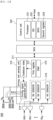
- FIG. 2 is a block diagram of a touch input device according to a first embodiment of the present invention, including a display panel 100, a touch controller 200, and a display controller 300.
- the display panel 100 includes a touch sensor 150, the touch controller 200 includes a driving and sensing unit 210 and a control unit 220, and the display controller 300 includes a gate driving circuit 310, a display control unit 320, and a data driving circuit 330.
- FIG. 3 are views for explaining multi-driving of the touch sensor 150 illustrated in FIG. 2 .
- the touch control unit 200 controls the touch sensor 150.
- the touch controller 200 may sequentially supply a driving signal to a plurality of driving electrodes of the touch sensor 150 or simultaneously supply a predetermined driving signal to at least two driving electrodes among the plurality of driving electrodes.
- the former is called as a sequential driving method, and the latter is called as a multi-driving method.
- the touch controller 200 receives a sensing signal output from the plurality of receiving electrodes of the touch sensor 150.
- the sensing signal may include information on an amount of capacitance variation between the receiving electrode and the driving electrode adjacent thereto, a low ground mass (LGM) noise signal, and a display noise signal.
- LGM low ground mass
- the touch controller 200 may analog-to-digital convert the sensing signal output from the plurality of receiving electrodes to output a digital sensing signal.
- the touch controller 200 may output two differential signals among the sensing signals output from the plurality of receiving electrodes and perform analog-to-digital conversion on the output differential signals.
- the touch controller 200 may include a comparator and an ADC.
- the touch controller 200 may detect whether a touch is generated and/or a touch position based on the digital signal output from the touch controller 200.
- the control unit 200 may be realized as one module, unit, or chip.
- the touch controller 200 may be divided into: a driving and sensing unit 210 that applies a driving signal to the driving electrode of the touch sensor 150 and receives a sensing signal from the receiving electrode of the touch sensor 150; and a control unit 220 that controls the driving and sensing unit 210.
- the driving and sensing unit 210 and the control unit 220 may be realized as one module, unit, or chip.
- the touch input device in FIG. 2 may include a display panel 100.
- a plurality of scan lines (or gate lines) and a plurality of data lines may be disposed on the display panel 100.
- a subpixel may be disposed in an area in which the scan line crosses the data line.
- the display panel 100 may include an active area on which a plurality of subpixels are disposed and an inactive area disposed outside the active area.
- the active area may constitute a display screen of the touch input device.
- the display screen may have a rectangular shape in which a horizontal length is greater than a vertical length.
- the touch input device illustrated in FIG. 2 may include the display controller 300 including the gate driving circuit 310, the display control unit 320, and the data driving circuit 330 for driving all sorts of signal lines disposed on the display panel 100 in order to drive the display panel 100.
- the gate driving circuit 310 may be controlled by the display control unit 320 and control a driving timing of a plurality of subpixels by sequentially outputting a display scan signal to the plurality of scan lines disposed on the display panel 100.
- the data driving circuit 330 may receive image data from the display control unit 320 and convert the image data into an analog type data voltage.
- the data driving circuit 330 may control each subpixel to display brightness according to the image data by outputting the data voltage (Vdata) to each data line in accordance with a timing when the scan signal is applied through the scan line.
- the display control unit 320 may supply all sorts of control signals to the gate driving circuit 310 and the data driving circuit 330 and control operations of the gate driving circuit 310 and the data driving circuit 330.
- the display control unit 320 may be provided separately from or integrated with the control unit 220 illustrated in FIG. 2 .
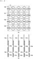
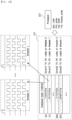
- FIG. 3 is a plan view illustrating a portion of an embodiment of the touch sensor 150 in FIG. 2 .
- FIG. 4 is plan views illustrating a state in which the touch sensor in FIG. 3 is separated by layers.
- FIG. 5 is a view for explaining electrical connection of a plurality of receiving electrodes in FIG. 4 .
- the touch sensor according to an embodiment of the present invention may be disposed on or in the display panel.
- the touch sensor according to the first embodiment of the present invention includes a plurality of first electrodes and a plurality of second electrodes.
- electrodes to which the driving signal is applied may serve as the driving electrodes, and the rest electrodes may serve as the receiving electrodes.
- the plurality of first electrodes serve as a plurality of driving electrodes TX0, TX1, TX2, TX3...
- the plurality of second electrodes serve as a plurality of receiving electrodes RX0, RX1, RX2, RX3, RX4....
- the plurality of driving electrodes TX0, TX1, TX2, TX3,... may include a 0-th driving electrode TX0, a first driving electrode TX1, a second driving electrode TX2, and a third driving electrode TX3.
- the plurality of driving electrodes TX0, TX1, TX2, TX3... correspond to the plurality of driving electrodes TX0, TX1, TX2,... illustrated in FIG. 2 .
- the plurality of receiving electrodes RX0, RX1, RX2, RX3, RX4,... may include a 0-th receiving electrode RX0, a first receiving electrode RX1, a second receiving electrode RX2, a third receiving electrode RX3, and a fourth receiving electrode RX4.
- the plurality of receiving electrodes RX0, RX1, RX2, RX3, RX4,... correspond to the plurality of receiving electrodes RX0, RX1, Rx2, Rx4,... illustrated in FIG. 2 .
- the plurality of driving electrodes TX0, TX1, TX2, TX3..,... may be arranged in a second direction (or vertical direction) and each extend in a first direction (or horizontal direction) perpendicular to the second direction.
- the plurality of receiving electrodes RX0, RX1, RX2, RX3, RX4,... may be arranged in the second direction.
- a predetermined capacitance may be formed between the plurality of driving electrodes TX0, TX1, TX2, TX3,... and the plurality of receiving electrodes RX0, RX1, RX2, RX3, RX4,....
- the capacitance is varied when a touch input is generated at a corresponding point or a surrounding thereof.
- whether a touch is generated or a touch input may be detected by detecting an amount of variation in capacitance from a signal output from the plurality of receiving electrodes RX0, RX1, RX2, RX3, RX4,....
- Each of the plurality of driving electrodes TX0, TX1, TX2, TX3... may have a rectangular pattern or bar pattern shape extending in the first direction and have a plurality of openings O disposed adjacent thereto and arranged in the first direction.
- One receiving electrode may be disposed in each opening O.
- Each opening O has a shape corresponding to that of one receiving electrode disposed adjacent thereto.
- the rest except for openings disposed on left and right edges among the plurality of openings O may have a rhombus shape, and the openings disposed on the left and right edges may each have a triangular shape.
- each of the openings O may have a rhombus shape.
- each of the plurality of openings O may have various shapes such as a polygon, a rectangle, a circle or an oval.
- Each of the receiving electrodes RX0, RX1, RX2, RX3, RX4,... includes a plurality of receiving electrode patterns RX0a, RX0b, RX1a, RX1b, RX2a, RX2b, RX3a, RX3b, RX4a, and RX4b and connecting patterns P0, P1, P2, P3, and P4.
- some receiving electrode patterns RX0a, RX1a, RX2a, RX3a, and RX4a among the plurality of receiving electrode patterns RX0a, RX0b, RX1a, RX1b, RX2a, RX2b, RX3a, RX3b, RX4a, and RX4b may correspond to the some receiving electrodes Rx0a, Rx1a, Rx2a, Rx3a,... in FIG. 2
- the rest receiving electrode patterns RX0b, RX1b, RX2b, RX3b, and RX4b may correspond to the rest receiving electrodes Rx0b, Rx1b, Rx2b, Rx3b,... in FIG. 2 .
- the plurality of driving electrodes TX0, TX1, TX2, TX3... and the plurality of receiving electrode patterns RX0a, RX0b, RX1a, RX1b, RX2a, RX2b, RX3a, RX3b, RX4a, and RX4b may be disposed together on a first layer.
- the plurality of driving electrodes TX0, TX1, TX2, TX3... and the plurality of receiving electrode patterns RX0a, RX0b, RX1a, RX1b, RX2a, RX2b, RX3a, RX3b, RX4a, and Rx4b, which are disposed on the first layer, may be made of a metal mesh.
- a plurality of connecting patterns P0a, P0b, P1a, P1b, P2a, P2b, P3a, P3b, P4a, and P4b may be disposed on a second layer.
- the second layer is different from the first layer in (a) of FIG. 4 and electrically insulated from the first layer.
- the plurality of connecting patterns P0a, P0b, P1a, P1b, P2a, P2b, P3a, P3b, P4a, and P4b may be made of a metal mesh.
- the first layer of (a) of FIG. 4 may be disposed on the second layer of (b) of FIG. 4 , and vice versa.
- the plurality of receiving electrode patterns contained in each receiving electrode may be divided into at least two groups.
- the receiving electrode patterns of another group are alternately arranged between the receiving electrode patterns of one group.
- the receiving electrode patterns of the one group are electrically separated from the receiving electrode patterns in the another group.
- the receiving electrode pattern in the one group may be referred to as a first receiving electrode pattern
- the receiving electrode pattern in the another group may be referred to as a second receiving electrode pattern.
- the plurality of connection patterns contained in each receiving electrode include first connection patterns that electrically connect the first receiving electrode patterns in the one group and second connection patterns that electrically connect the second receiving electrode patterns in the other group.
- each of the first connection patterns P0a electrically connects two adjacent receiving electrode patterns RX0a through the conductive via v among the receiving electrode patterns RX0a of the first group and is disposed below the receiving electrode patterns RX0b of the second group, which are disposed between the two adjacent receiving electrode patterns RX0a, to overlap the receiving electrode patterns RX0b of the second group.
- the driving signal When the driving signal is applied sequentially or simultaneously to the plurality of driving electrodes TX0, TX1, TX2, and TX3, two sensing signals are output through the first connection pattern P1.
- a first signal is output through the first connection pattern P1a, and a second signal is output through the second connection pattern P1b.
- the second signal output through the second connection pattern P1b serves as the active channel signal
- the first signal output through the first connection pattern P1a serves as the dummy channel signal
- a capacitance (or mutual active capacitance) formed between the first driving electrode TX1 and the receiving electrode pattern RX1b of the second group of the first receiving electrode RX1 is varied.
- the second signal including information on an amount of variation of the varied capacitance is an active channel signal output through the second connection pattern P1b.
- the driving and sensing unit 210 illustrated in FIG. 2 may subtract the first signal output through the first connection pattern P1a from the second signal output through the second connection pattern P1b to cancel all or most of a cathode retransmission noise signal, a LGM noise signal, and a display noise signal input to the receiving electrode pattern RX1b of the second group and the receiving electrode pattern RX1a of the first group.
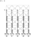
- FIG. 7 is plan views illustrating a state in which the touch sensor in FIG. 6 is separated by layers.
- the touch sensor according to another embodiment of the present invention illustrated in FIGS. 6 to 8 is different in a plurality of receiving electrodes RX0', RX1', RX2', RX3', and RX4' from the touch sensor according to an embodiment of the present invention illustrated in FIGS. 3 to 5 .
- a plurality of receiving electrode patterns RX1a' contained in each of the receiving electrodes RX0', RX1', RX2', RX3', and RX4' have different structures.
- the structures of the plurality of electrode patterns RX1a' will be described in detail, and the rest components will be replaced with those described above.
- Each of the plurality of receiving electrode patterns RX1a' contained in each of the receiving electrodes RX0', RX1', RX2', RX3', and RX4' has an opening O' therein and includes a dummy pattern DX1a disposed in the opening O'.
- the dummy pattern DX1a may have a shape corresponding to the opening O'.
- the dummy pattern DX1a is not electrically connected to connection patterns P0a, P0b, P1a, P1b, P2a, P2b, P3a, P3b, P4a, and P4b.
- the dummy pattern DX1a maintains an electrically floating state.
- An operation of the touch sensor illustrated in FIGS. 6 to 8 according to another embodiment of the present invention is the same as that of the touch sensor illustrated in FIGS. 3 to 5 according to an embodiment of the present invention.
- a touch input device including the touch sensor illustrated in FIGS. 6 to 8 has an advantage of removing various noises generated during touch sensing, e.g., the cathode retransmission noise signal, the display noise signal, and the LGM noise signal.
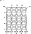
- FIG. 9 is a plan view illustrating a portion of another embodiment of the touch sensor 150 in FIG. 2 .
- FIG. 10 is plan views illustrating a state in which the touch sensor in FIG. 9 is separated by layers.
- the touch sensor according to another embodiment of the present invention illustrated in FIGS. 9 to 10 is different in a plurality of receiving electrodes RX0", RX1", RX2", RX3", and RX4" from the touch sensor according to an embodiment of the present invention illustrated in FIGS. 3 to 5 .
- connection patterns P0', P1', P2', P3', and P4' contained in each of the receiving electrodes RX0", RX1", RX2", RX3", and RX4" have different arrangement structures and shapes.
- the arrangement structures and shapes of the connection patterns P0', P1', P2', P3', and P4' will be described in detail, and the rest components will be replaced with those described above.
- connection patterns P0', P 1', P2', P3', and P4' includes first connection patterns P0a', P1a', P2a', P3a', and P4a' and second connection patterns P0b', P1b', P2b', P3b', and P4b'.
- Each of the first connection patterns P0a', P1a', P2a', P3a', and P4a' electrically connects two receiving electrode patterns RX0a, RX1a, RX2a, RX3a, and RX4a of the first group so as not to overlap the receiving electrode patterns RX0b, RX1b, RX2b, RX3b, and RX4b of the second group disposed between the two receiving electrode patterns.
- each of the first connection patterns P0a', P1a', P2a', P3a', and P4a' may be disposed between the receiving electrode patterns RX0b, RX1b, RX2b, and Rx3b of the second group and the driving electrodes TX0, TX1, TX2, and TX3 disposed directly adjacent to the receiving electrode patterns RX0b, RX1b, RX2b, and RX3b of the second group so as not to overlap the receiving electrode patterns RX0b, RX1b, RX2b, RX3b, and Rx4b of the second group.
- the rest portion may be disposed to overlap the driving electrodes TX0, TX1, TX2, and TX3.
- Each of the second connection patterns P0b', P1b', P2b', P3b', and P4b' electrically connects two receiving electrode patterns RX0a, RX1a, RX2a, RX3a, and RX4a of the second group so as not to overlap the receiving electrode patterns RX0a, RX1a, RX2a, RX3a, and RX4a of the first group disposed between the two receiving electrode patterns.
- each of the second connection patterns P0b', P1b', P2b', P3b', and P4b' may be disposed between the receiving electrode patterns RX0a, RX1a, RX2a, RX3a, and RX4a of the first group and the driving electrodes TX0, TX1, TX2, and TX3 disposed directly adjacent to the receiving electrode patterns RX0a, RX1a, RX2a, RX3a, and RX4a of the first group so as not to overlap the receiving electrode patterns RX0a, RX1a, RX2a, RX3a, and Rx4a of the first group.
- the rest portion may be disposed to overlap the driving electrodes TX0, TX1, TX2, and TX3.
- the touch sensor according to another embodiment of the present invention may have an advantage of reducing a capacitance value between the first connection patterns and the receiving electrode patterns of the second group or between the second connection patterns and the receiving electrode patterns of the first group in comparison with the touch sensor in FIGS. 3 to 5 according to an embodiment of the present invention.
- the dummy pattern DX1a in FIGS. 7 and 8 may be applied to the touch sensor according to another embodiment of the present invention.
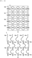
- FIG. 11 is a plan view illustrating a portion of another embodiment of the touch sensor 150 in FIG. 2 .
- FIG. 12 is plan views illustrating a state in which the touch sensor in FIG. 11 is separated by layers.
- the touch sensor according to another embodiment of the present invention illustrated in FIGS. 11 to 12 is different in a plurality of receiving electrodes RX0′′′, RX1′′′, RX2'", RX3'", and RX4'" from the touch sensor according to an embodiment of the present invention illustrated in FIGS. 3 to 5 .
- a plurality of receiving electrode patterns RX0a-1, RX0a-2, RX0b-1, RX0b-2, RX1a-1, RX1a-2, RX1b-1, RX1b-2, RX2a-1, RX2a-2, RX2b-1, RX2b-2, RX3a-1, RX3a-2, RX3b-1, and RX3b-2 and a plurality of connection patterns P0", P1", P2", and P3" contained in each of the receiving electrodes RX0'", RX1'", RX2'", and RX3′′′ have different structures and arrangement shapes.
- the structures and arrangement shapes of the receiving electrode patterns RX0a-1, RX0a-2, RX0b-1, RX0b-2, RX1a-1, RX1a-2, RX1b-1, RX1b-2, RX2a-1, RX2a-2, RX2b-1, RX2b-2, RX3a-1, RX3a-2, RX3b-1, and RX3b-2 and the connection patterns P0", P1", P2", and P3" will be described in detail, and the rest components will be replaced with those described above.
- the plurality of receiving electrode patterns RX0a-1, RX0a-2, RX0b-1, RX0b-2, RX1a-1, RX1a-2, RX1b-1, RX1b-2, RX2a-1, RX2a-2, RX2b-1, RX2b-2, RX3a-1, RX3a-2, RX3b-1, and RX3b-2 of each of the receiving electrodes RX0′′′, RX1'", RX2'", and RX3′′′ include the receiving electrode patterns RX0a-1, RX0a-2, RX1a-1, RX1a-2, RX2a-1, RX2a-2, RX3a-1, and RX3a-2 of the first group and the receiving electrode patterns RX0b-1, RX0b-2, RX1b-1, RX1b-2, RX2b-1, RX2b-2, RX3b-1, and Rx3b-2 of the second group, which are alternately arranged one
- the receiving electrode patterns RX0a-1, RX0a-2, RX1a-1, RX1a-2, RX2a-1, RX2a-2, RX3a-1, and RX3a-2 of the first group and the receiving electrode patterns RX0b-1, RX0b-2, RX1b-1, RX1b-2, RX2b-1, RX2b-2, RX3b-1, and RX3b-2 of the second group may be electrically separated from each other.
- Each of the first group of receiving electrode patterns RX0a-1, RX0a-2, RX1a-1, RX1a-2, RX2a-1, RX2a-2, RX3a-1, and RX3a-2 includes first receiving electrode patterns RX0a-1, RX1a-1, RX2a-1, and RX3a-1 and second receiving electrode patterns RX0a-2, RX1a-2, RX2a-2, and RX3a-2.
- the first receiving electrode patterns RX0a-1, RX1a-1, RX2a-1, and RX3a-1 and the second receiving electrode patterns RX0a-2, RX1a-2, RX2a-2, and RX3a-2 are disposed in two opening O adjacent to each other in the first direction in the corresponding driving electrodes TX0 and TX2, respectively.
- One first or second receiving electrode pattern is disposed in the openings disposed at both side edges among a plurality of openings O of each of the driving electrodes TX0, TX1, TX2, and TX3, and the second receiving electrode pattern of the first group of receiving electrode patterns of one receiving electrode and the first receiving electrode pattern of the first group of receiving electrode patterns of another receiving electrode are disposed together in the rest openings while being spaced apart from each other among the plurality of receiving electrodes RX0′′′, RX1′′′, RX2'", and RX3'".
- connection patterns P0", P1", P2", and P3 includes first connection patterns P0a”, P1a", P2a", and P3a” electrically connecting the receiving electrode patterns RX0a-1, RX0a-2, RX1a-1, RX1a-2, RX2a-1, RX2a-2, RX3a-1, and RX3a-2 of the first group and second connection patterns P0b", P1b", P2b", and P3b” electrically connecting the receiving electrode patterns RX0b-1, RX0b-2, RX1b-1, RX1b-2, RX2b-1, RX2b-2, RX3b-1, and Rx3b-2 of the second group.
- Each of the first connection patterns P0a”, P1a”, P2a”, and P3a” and the second connection patterns P0b”, P1b", P2b", and P3b" are configured and arranged to connect two adjacent receiving electrode patterns for each group with a minimum distance.
- each of the first connection patterns P0a”, P1a”, P2a”, and P3a” further includes a receiving connection pattern electrically connecting the first receiving electrode pattern and the second receiving electrode pattern of the first group of receiving electrode patterns
- each of the second connection patterns P0b”, P1b", P2b", and P3b” further includes a receiving connection pattern electrically connecting the first receiving electrode pattern and the second receiving electrode pattern of the second group of receiving electrode patterns.
- the touch sensor according to another embodiment of the present invention may have an advantage of reducing a capacitance value between the first connection patterns and the receiving electrode patterns of the second group or between the second connection patterns and the receiving electrode patterns of the first group in comparison with the touch sensor in FIGS. 3 to 5 according to an embodiment of the present invention.
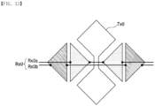
- a touch sensor in FIG. 13 includes a plurality of driving electrodes Tx0 and a plurality of receiving electrodes Rx0.
- Each of driving electrodes Tx0 includes diamond-shaped pattern parts arranged along one direction, and a connection pattern part connecting two adjacent pattern parts of the pattern parts to each other.
- Each of receiving electrodes Rx0 includes a first electrode part RxOa and a second electrode part Rx0b arranged along a direction different from the one direction.
- Each of the first electrode part RxOa and the second electrode part Rx0b may have a triangular shape.
- One first electrode part RxOa and one second electrode part Rx0b, which are disposed adjacent to each other, may have an overall diamond shape.
- the first electrode part RxOa is relatively closer to the driving electrode Tx0 than the second electrode part Rx0b.
- the second electrode part Rx0b is relatively closer to another driving electrode than the first electrode part RxOa.
- the first electrode parts RxOa may be electrically connected to each other through a plurality of conductive traces.
- the second electrode parts Rx0b may be electrically connected to each other through a plurality of conductive traces.
- the touch input device illustrated in FIG. 14 has a difference in comparison with the touch input device according to the first embodiment illustrated in FIG. 2 as stated below.
- a touch sensor 150' of the touch input device illustrated in FIG. 14 includes electrodes each having a predetermined shape, and the predetermined electrodes include a plurality of first electrodes and a plurality of second electrodes.
- the plurality of first electrodes serve as the plurality of driving electrodes Tx0, Tx1, Tx2,...
- the plurality of second electrodes serve as the plurality of receiving electrodes Rx0, Rx1, Rx2,...
- a plurality of first electrodes serve as a plurality of receiving electrodes Rx0, Rx1, Rx2,...
- a plurality of second electrodes serve as a plurality of driving electrodes Tx0, Tx1, Tx2,....
- the plurality of driving electrodes Tx0, Tx1, Tx2,... are replaced with the plurality of receiving electrodes Rx0, Rx1, Rx2,..., and the plurality of receiving electrodes Rx0, Rx1, Rx2,... are replaced with the plurality of driving electrodes Tx0, Tx1, Tx2,....
- the feature in which the plurality of first electrodes serve as the plurality of driving electrodes as illustrated in FIG. 2 or serve as the plurality of receiving electrodes as illustrated in FIG. 14 may be determined by control of a control unit 220.
- the plurality of first electrodes may serve as the plurality of driving electrodes
- the plurality of second electrodes may serve as the plurality of driving electrodes
- the plurality of driving electrodes Tx0, Tx1, Tx2,... and the plurality of receiving electrodes Rx0, Rx1, Rx2,... may be arranged to cross each other.
- Each of the driving electrodes Tx0, Tx1, Tx2,... may extend in a second axis direction
- each of the receiving electrode Rx0, Rx1, Rx2,... may extend in a first axis direction different from the second axis direction.
- the first axis direction may be perpendicular to the second axis direction.
- Some driving electrodes Tx0a, Tx1a, Tx2a, Tx3a,... among the plurality of driving electrodes Tx0, Tx1, Tx2,... may be arranged to form a mutual capacitance Cm with even-numbered receiving electrodes Rx0, Rx2, Rx4, Rx6,... among the plurality of receiving electrodes Rx0, Rx1, Rx2,..., and the rest driving electrodes Tx0, Tx1, Tx2,... among the plurality of driving electrodes Tx0, Tx1, Tx2,... may be arranged to form a mutual capacitance Cm with odd-numbered receiving electrodes Rx1, Rx3, Rx5, Rx7,... among the plurality of receiving electrodes Rx0, Rx1, Rx2,....
- Some driving electrodes Tx0a, Tx1a, Tx2a, Tx3a,... among the plurality of driving electrodes Tx0, Tx1, Tx2,... may be arranged directly adjacent to the even-numbered receiving electrodes Rx0, Rx2, Rx4, Rx6,... among the plurality of receiving electrodes Rx0, Rx1, Rx2,... and spaced a predetermined distance from the odd-numbered receiving electrodes Rx1, Rx3, Rx5, Rx7,... among the plurality of receiving electrodes Rx0, Rx1, Rx2,... instead of being directly adjacent thereto.
- At least one different electrode may be disposed between the some driving electrodes Tx0a, Tx1a, Tx2a, Tx3a,... and the rest odd-numbered receiving electrodes Rx1, Rx3, Rx5, Rx7,....
- the different electrode may be the even-numbered receiving electrodes Rx0, Rx2, Rx4, Rx6,....
- the rest driving electrodes Tx0b, Tx1b, Tx2b, Tx3b,... among the driving electrodes Tx0, Tx1, Tx2,... may be arranged directly adjacent to the rest receiving odd-numbered electrodes Rx1, Rx3, Rx5, Rx7,... among the plurality of receiving electrodes Rx0, Rx1, Rx2,... and spaced a predetermined distance from the even-numbered receiving electrodes Rx0, Rx2, Rx4, Rx6,... instead of being directly adjacent thereto.
- At least one different electrode may be disposed between the rest driving electrodes Tx0b, Tx1b, Tx2b, Tx3b,... and the some even-numbered receiving electrodes Rx0, Rx2, Rx4, Rx6,....
- the different electrode may be the rest odd-numbered receiving electrodes Rx1, Rx3, Rx5, Rx7,....
- the driving signal applied to the rest driving electrodes Tx0b, Tx1b, Tx2b, Tx3b,... may be an inverted driving signal obtained by inverting only a phase by 180° from the driving signal applied to some driving electrodes Tx0a, Tx1a, Tx2a, Tx3a,....
- a driving signal applied to the driving electrode TxOb of two driving electrodes TxOa and TxOb of 0-th driving electrodes Tx0 may be an inverted driving signal obtained by inverting the driving signal applied to TxOa.
- the touch input device illustrated in FIG. 14 may perform a multi-driving of simultaneously applying driving signals to all driving electrodes Tx0, Tx1, Tx2, Tx3,... of the touch sensor 150', and a flicker does not occur on the display panel although the multi-driving is performed.
- a driving time for performing mutual sensing may be reduced.
- a turn-on time of an analog front end (AFE) may be reduced, power consumption may be further reduced.
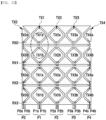
- FIG. 15 is a plan view illustrating a portion of an embodiment of the touch sensor 150' illustrated in FIG. 13 .
- An embodiment of the touch sensor 150' illustrated in FIG. 15 has the same structure of a plurality of electrodes as an embodiment of the touch sensor 150 illustrated in FIG. 3 , but has a difference in that the driving electrodes TX0, TX1, TX2, TX3, and TX4 to which the driving signal is applied and the receiving electrodes RX0, RX1, RX2, and RX3 through which the receiving signal is output are reversely provided.
- the control unit 220 illustrated in FIG. 14 may control predetermined driving signals to be applied simultaneously to the connection patterns P0, P1, P2, P3, P4,... of the plurality of driving electrodes TX0, TX1, TX2, TX3, TX4,....
- the driving signal applied to the second connection pattern P0b of each of the connection patterns P0 is an inverted driving signal having a phase inverted by 180° from the driving signal applied to the first connection pattern P0a.
- the control unit 220 illustrated in FIG. 14 may receive receiving signals having information on an amount of variation in mutual capacitance from the plurality of receiving electrodes RX0, RX1, RX2, RX3,... and output differential signals from the received receiving signals. Then, the received signals received from the plurality of receiving electrodes RX0, RX1, RX2, RX3,... may be restored by integrating the differential signals, and a touch position of an object may be determined based on the information on the amount of variation in mutual capacitance, in which signs of the restored receiving signals are processed.
- FIG. 16 is a plan view illustrating a portion of another embodiment of the touch sensor 150' illustrated in FIG. 14 .
- FIG. 16 Another embodiment of the touch sensor 150' illustrated in FIG. 16 has the same structure of a plurality of electrodes as an embodiment of the touch sensor 150 illustrated in FIG. 2 , but has a difference in that the driving electrodes to which the driving signal is applied and the receiving electrodes through which the receiving signal is output are reversely provided.
- the control unit 220 illustrated in FIG. 14 may control predetermined driving signals to be applied simultaneously to the connection patterns P0, P1, P2, P3, P4,... of the plurality of driving electrodes TX0, TX1, TX2, TX3, TX4,....
- the driving signal applied to the second connection pattern P0b of each of the connection patterns P0 is an inverted driving signal having a phase inverted by 180° from the driving signal applied to the first connection pattern P0a.
- the control unit 220 illustrated in FIG. 14 may receive receiving signals having information on an amount of variation in mutual capacitance from the plurality of receiving electrodes RX0, RX1, RX2, RX3,... and output differential signals from the received receiving signals.
- the receiving signals received from the plurality of receiving electrodes RX0, RX1, RX2, RX3,... may be restored again by integrating the differential signals, and a touch position of an object may be determined based on the information on the amount of variation in mutual capacitance, in which signs of the restored receiving signals are processed.
- FIG. 17 Another embodiment of the touch sensor 150' illustrated in FIG. 17 has the same structure of a plurality of electrodes as another embodiment of the touch sensor 150 illustrated in FIG. 9 , but has a difference in that the driving electrodes to which the driving signal is applied and the receiving electrodes through which the receiving signal is output are reversely provided.
- the control unit 220 illustrated in FIG. 14 may control predetermined driving signals to be applied simultaneously to the connection patterns P0', P1', P2', P3', P4',... of the plurality of driving electrodes TX0", TX1", TX2", TX3", TX4",....
- the driving signal applied to the second connection pattern P0b of each of the connection patterns P0' is an inverted driving signal having a phase inverted by 180° from the driving signal applied to the first connection pattern P0a.
- the control unit 220 illustrated in FIG. 14 may receive receiving signals having information on an amount of variation in mutual capacitance from the plurality of receiving electrodes RX0, RX1, RX2, RX3,... and output differential signals from the received receiving signals.
- the receiving signals received from the plurality of receiving electrodes RX0, RX1, RX2, RX3,... may be restored again by integrating the differential signals, and a touch position of an object may be determined based on the information on the amount of variation in mutual capacitance, in which signs of the restored receiving signals are processed.
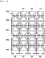
- FIG. 18 is a plan view illustrating a portion of another embodiment of the touch sensor 150' illustrated in FIG. 14 .
- FIG. 18 Another embodiment of the touch sensor 150' illustrated in FIG. 18 has the same structure of a plurality of electrodes as another embodiment of the touch sensor 150 illustrated in FIG. 11 , but has a difference in that the driving electrodes to which the driving signal is applied and the receiving electrodes through which the receiving signal is output are reversely provided.
- the control unit 220 illustrated in FIG. 14 may control predetermined driving signals to be applied simultaneously to the connection patterns P0", P1", P2", P3",... of the plurality of driving electrodes TX0'", TX1′′′, TX2′′′, TX3′′′,....
- the driving signal applied to the second connection pattern P0b of each of the connection patterns P0" is an inverted driving signal having a phase inverted by 180° from the driving signal applied to the first connection pattern P0a.
- the control unit 220 illustrated in FIG. 14 may receive receiving signals having information on an amount of variation in mutual capacitance from the plurality of receiving electrodes RX0, RX1, RX2, RX3,... and output differential signals from the received receiving signals.
- the receiving signals received from the plurality of receiving electrodes RX0, RX1, RX2, RX3,... may be restored again by integrating the differential signals, and a touch position of an object may be determined based on the information on the amount of variation in mutual capacitance, in which signs of the restored receiving signals are processed.
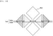
- FIG. 19 is a plan view illustrating a portion of another embodiment of the touch sensor 150' illustrated in FIG. 14 .
- FIG. 19 Another embodiment of the touch sensor illustrated in FIG. 19 has the same structure of a plurality of electrodes as an embodiment of the touch sensor illustrated in FIG. 18 , but has a difference in that the driving electrodes to which the driving signal is applied and the receiving electrodes through which the receiving signal is output are reversely provided.
- control unit 200 illustrated in FIG. 14 may control predetermined driving signals to be applied simultaneously to the first driving electrode part TxOa and the second driving electrode part TxOb of the plurality of driving electrodes Tx0.
- the driving signal applied to the first driving electrode part TxOa is an inverted driving signal having a phase inverted by 180° from the driving signal applied to the second driving electrode part TxOb.
- the control unit 200 illustrated in FIG. 14 may receive receiving signals having information on an amount of variation in mutual capacitance from the plurality of receiving electrodes RX0, RX1, RX2, RX3,... and output differential signals from the received receiving signals.
- the receiving signals received from the plurality of receiving electrodes RX0, RX1, RX2, RX3,... may be restored again by integrating the differential signals, and a touch position of an object may be determined based on the information on the amount of variation in mutual capacitance, in which signs of the restored receiving signals are processed.
- FIG. 20 are views for explaining the multi-driving of the touch sensor 150 illustrated in FIG. 2 .
- FIG. 21 is a block diagram of a touch controller in the touch input device illustrated in FIG. 2 and includes a driving and sensing unit 210 and a control unit 220.
- the driving and sensing unit 210 includes a codebook table 211, a first register 212, a DMA 213, a driving signal generation part 214, and a plurality of sensing sensors 215, and the control unit 220 includes a processor 221, an external serial interface 222, a general-purpose input/output part 223, and a second register 224.
- FIG. 22 is a view illustrating an output waveform of the driving signal generation part in the driving and sensing unit illustrated in FIG. 21 and a corresponding codebook matrix.
- FIG. 23 is a view illustrating an output waveform of the driving signal generation part in the driving and sensing unit illustrated in FIG. 21 and a corresponding codebook matrix.
- FIG. 24 is a view illustrating an output waveform of the driving signal generation part operating according to an exemplary value of the codebook table in the driving and sensing unit illustrated in FIG. 21 .
- the multi-driving of the touch sensor 150 illustrated in FIG. 2 may simultaneously apply (Touch Scan 1) a predetermined driving signal to four driving electrodes Tx0, Tx1, Tx2, and Tx3 in a predetermined first time period, simultaneously apply (Touch Scan 2) the driving signal to other four driving electrodes Tx4, Tx5, Tx6, and Tx7 in a second time period after the first time period, and simultaneously apply (Touch Scan 3) the driving signal to other four driving electrodes Tx8, Tx9, Tx10, and Tx11 in a third time period after the second time period.
- Touch Scan 1 a predetermined driving signal to four driving electrodes Tx0, Tx1, Tx2, and Tx3 in a predetermined first time period
- Touch Scan 2 the driving signal to other four driving electrodes Tx4, Tx5, Tx6, and Tx7 in a second time period after the first time period
- Touch Scan 3 the driving signal to other four driving electrodes Tx8, Tx9, Tx10,
- the multi-driving of the touch sensor 150 may simultaneously apply (Touch Scan 4) the driving signal to other four driving electrodes Tx12, Tx13, Tx14, and Tx15 in a fourth time period after the third time period and simultaneously apply (Touch Scan 5) the driving signal to other four driving electrodes Tx16, Tx17, Tx18, and Tx19 in a fifth time period after the fourth time period.
- Touch Scan 4 the driving signal to other four driving electrodes Tx12, Tx13, Tx14, and Tx15 in a fourth time period after the third time period
- Touch Scan 5 the driving signal to other four driving electrodes Tx16, Tx17, Tx18, and Tx19 in a fifth time period after the fourth time period.
- areas of Touch Scans indicate areas of four driving electrodes to which four driving signals are simultaneously applied during the same time period for convenience of explanation.
- FIG. 20 is an example of driving signals that are simultaneously applied to the four driving electrodes in each Touch Scan.
- Each of the driving signals may be obtained by continuing a vector value expressed as either -1, 0, or 1 for each predetermined time period t1, t2, t3, and t4 as many as the number of the driving electrodes.
- driving signals having vector values of 1, 1, 1, and -1 are simultaneously applied to the driving electrodes Tx0, Tx1, Tx2, and Tx3 in the first time period t1
- driving signals having vector values of 1, 1, -1, and 1 are simultaneously applied to the driving electrodes Tx0, Tx1, Tx2, and Tx3 in the second time period t2
- driving signals having vector values of 1, -1, 1, and 1 are simultaneously applied to the driving electrodes Tx0, Tx1, Tx2, and Tx3 in the third time period t3
- driving signals having vector values of -1, 1, 1, and 1 are simultaneously applied to the driving electrodes Tx0, Tx1, Tx2, and Tx3 in the fourth time period t4.
- the vector value '1' and the vector value '-1' are vector values of each row and each column constituting the codebook matrix as in FIG. 22 .
- the vector value '1' maintains a phase of the driving signal, and the vector value '-1' inverts the phase of the driving signal.
- the codebook matrix may be stored as a 5 x 5 matrix or more.
- the codebook table 211 matches a plurality of codes programmed by firmware built in the processor 221 with a plurality of addresses, respectively, and store the matched codes.
- the codebook table that is a table capable of storing data such as internal and external memory or logic registers of a touch controller such as SRAM or NVM collects code vectors for encoding and/or decoding of data.
- the plurality of codes may include binary data having a predetermined bit of a driving signal scanned for each time slot.
- the number of codes x (the number of Tx x 2) codes may be stored in advance in the first register 212 (or SRAM).
- the code has a length of 128 x 40.
- 2 bits may be allocated for each driving signal channel (TX CH) to control a combination of codes.
- 00b may be set as a low level signal
- 01b may be set as a pulse signal
- 10b may be set as a high level signal
- 11b may be set as an inverse pulse signal, which are stored in the first register 212.
- a pulse, a pulse, a pulse, and a reverse pulse are applied as matched and set to the first register 212 that is the codebook register, and a waveform illustrated at an upper end of FIG. 23 is output to each time slot of the driving electrodes Tx0, Tx1, Tx2, and Tx3.
- the first register 212 receives a plurality of addresses and data matched with the respective addresses from the codebook table 211 and temporarily stores the addresses and data.
- the DMA (direct memory access) 213 receives necessary data by directly accessing the first register 212 from a peripheral device instead of being processed by the built-in processor 221.
- the driving signal generation part 214 receives a plurality of codes stored in advance according to each scan mode from the codebook table 211 and generates a driving signal (or Tx signal) to output the generated driving signal to the driving electrode (Tx electrode) of the touch sensor 150.
- the driving signal may include a low level signal, a pulse signal, a high level signal, and a reverse pulse signal.
- the plurality of sensing sensors 215 sense a touch of a user through the plurality of receiving electrodes and output a sensing signal.
- the processor 221 sets the start codebook address when scanning is performed according to the scan mode through the built-in firmware and programs each code with a combination of predetermined bits. Also, whenever the first register 212 is controlled, the corresponding code may be read and written in the codebook table 211.
- the codebook table 211 may store various kinds of codes in advance according to the scan mode and set the start codebook address when the scanning is performed.
- the external serial interface (ESI) 222 is an input/output interface that transmits data calculated by the processor 221 to a host and receives data from the host to transmit the received data to the processor 221.
- the general-purpose input/output part (GPIO) 223 has an input or output operation controlled by the user during a runtime.
- the second register 224 temporarily stores data input or output through the general input/output part 223.
- the present invention may recognize an address to be started for each scan according to each scan mode to perform various operations according to information on the driving signal matched with and stored at the address and control the driving signals performed at the same time regardless of the number of driving signals.
- the present invention may perform various touch sensings using the single touch controller by storing various code values in advance in the codebook according to the touch scan mode in the touch input device.
- the touch driving time and sensing time of the touch input device may be reduced without performing additional firmware calculations whenever the code change is required or whenever the touch input device performs the touch driving.
- the central processing unit may perform other important operations during the code change, the operation efficiency of the central processing unit may increase, the power consumption may be saved, and the decrease phenomenon of the reporting rate may be prevented.
Landscapes
- Engineering & Computer Science (AREA)
- General Engineering & Computer Science (AREA)
- Theoretical Computer Science (AREA)
- Human Computer Interaction (AREA)
- Physics & Mathematics (AREA)
- General Physics & Mathematics (AREA)
- Position Input By Displaying (AREA)
Applications Claiming Priority (1)
| Application Number | Priority Date | Filing Date | Title |
|---|---|---|---|
| KR1020230089837A KR20250009782A (ko) | 2023-07-11 | 2023-07-11 | 터치 입력 장치 |
Publications (1)
| Publication Number | Publication Date |
|---|---|
| EP4492208A1 true EP4492208A1 (fr) | 2025-01-15 |
Family
ID=91481658
Family Applications (1)
| Application Number | Title | Priority Date | Filing Date |
|---|---|---|---|
| EP24181531.5A Pending EP4492208A1 (fr) | 2023-07-11 | 2024-06-11 | Dispositif d'entrée tactile |
Country Status (5)
| Country | Link |
|---|---|
| US (1) | US20250021179A1 (fr) |
| EP (1) | EP4492208A1 (fr) |
| JP (2) | JP7748750B2 (fr) |
| KR (1) | KR20250009782A (fr) |
| CN (1) | CN119311147A (fr) |
Citations (4)
| Publication number | Priority date | Publication date | Assignee | Title |
|---|---|---|---|---|
| US20160313823A1 (en) * | 2015-04-22 | 2016-10-27 | Stmicroelectronics Asia Pacific Pte Ltd | Capacitive touch screen with time overlapped concurrent scanning operation using coded drive signals |
| US20210141474A1 (en) * | 2018-04-24 | 2021-05-13 | Synaptics Incorporated | Spatially encoded sensor electrodes |
| US20220326831A1 (en) * | 2021-04-13 | 2022-10-13 | Samsung Display Co., Ltd. | Touch sensor and a display device including the same |
| KR102499519B1 (ko) * | 2021-09-17 | 2023-02-16 | 주식회사 하이딥 | 터치 센서 및 이를 포함하는 터치 입력 장치 |
Family Cites Families (5)
| Publication number | Priority date | Publication date | Assignee | Title |
|---|---|---|---|---|
| KR102325034B1 (ko) * | 2017-06-02 | 2021-11-10 | 엘지디스플레이 주식회사 | 터치 디스플레이 장치 및 터치 디스플레이 장치의 구동 방법 |
| KR102385632B1 (ko) * | 2017-10-31 | 2022-04-11 | 엘지디스플레이 주식회사 | 터치 디스플레이 장치 |
| KR102479079B1 (ko) * | 2017-12-29 | 2022-12-19 | 엘지디스플레이 주식회사 | 터치표시장치, 터치구동회로 및 터치구동방법 |
| KR102468750B1 (ko) * | 2017-12-29 | 2022-11-18 | 엘지디스플레이 주식회사 | 터치표시장치, 터치시스템, 터치구동회로, 펜 및 펜 센싱 방법 |
| KR102488630B1 (ko) * | 2018-07-13 | 2023-01-16 | 엘지디스플레이 주식회사 | 터치 표시 패널, 터치 표시 장치 |
-
2023
- 2023-07-11 KR KR1020230089837A patent/KR20250009782A/ko active Pending
-
2024
- 2024-05-22 JP JP2024083318A patent/JP7748750B2/ja active Active
- 2024-06-11 EP EP24181531.5A patent/EP4492208A1/fr active Pending
- 2024-06-25 CN CN202410826529.2A patent/CN119311147A/zh active Pending
- 2024-07-11 US US18/770,242 patent/US20250021179A1/en active Pending
-
2025
- 2025-09-12 JP JP2025152379A patent/JP2025176140A/ja active Pending
Patent Citations (5)
| Publication number | Priority date | Publication date | Assignee | Title |
|---|---|---|---|---|
| US20160313823A1 (en) * | 2015-04-22 | 2016-10-27 | Stmicroelectronics Asia Pacific Pte Ltd | Capacitive touch screen with time overlapped concurrent scanning operation using coded drive signals |
| US20210141474A1 (en) * | 2018-04-24 | 2021-05-13 | Synaptics Incorporated | Spatially encoded sensor electrodes |
| US20220326831A1 (en) * | 2021-04-13 | 2022-10-13 | Samsung Display Co., Ltd. | Touch sensor and a display device including the same |
| KR102499519B1 (ko) * | 2021-09-17 | 2023-02-16 | 주식회사 하이딥 | 터치 센서 및 이를 포함하는 터치 입력 장치 |
| US20240264700A1 (en) * | 2021-09-17 | 2024-08-08 | Hideep Inc. | Touch sensor and touch input device comprising same |
Also Published As
| Publication number | Publication date |
|---|---|
| CN119311147A (zh) | 2025-01-14 |
| KR20250009782A (ko) | 2025-01-20 |
| US20250021179A1 (en) | 2025-01-16 |
| JP7748750B2 (ja) | 2025-10-03 |
| JP2025176140A (ja) | 2025-12-03 |
| JP2025013174A (ja) | 2025-01-24 |
Similar Documents
| Publication | Publication Date | Title |
|---|---|---|
| CN110362223B (zh) | 触摸控制器、触摸感测设备和触摸感测方法 | |
| JP2025148575A (ja) | タッチセンサ及びこれを含むタッチ入力装置 | |
| US20190243485A1 (en) | Touch input device | |
| US20260072539A1 (en) | Touch input device | |
| JP7724580B2 (ja) | タッチ入力装置 | |
| US20250021179A1 (en) | Touch input device | |
| CN118860177A (zh) | 显示装置和驱动该显示装置的方法 | |
| US20240345674A1 (en) | Touch sensor and touch input device thereof | |
| US20250093998A1 (en) | Touch input device | |
| EP4478164A1 (fr) | Capteur tactile et dispositif d'entrée tactile le comprenant | |
| CN113268160A (zh) | 一种触控显示面板及其驱动方法、触控显示装置 | |
| KR102758467B1 (ko) | 터치 입력 장치 | |
| KR102846192B1 (ko) | 터치 입력 장치 | |
| US20240377906A1 (en) | Sensor Module and Control Method for Sensor Module | |
| KR102916015B1 (ko) | 터치 입력 장치 | |
| CN210402294U (zh) | Pmoled显示装置及电子设备 | |
| KR20240076238A (ko) | 터치 입력 장치 |
Legal Events
| Date | Code | Title | Description |
|---|---|---|---|
| PUAI | Public reference made under article 153(3) epc to a published international application that has entered the european phase |
Free format text: ORIGINAL CODE: 0009012 |
|
| STAA | Information on the status of an ep patent application or granted ep patent |
Free format text: STATUS: REQUEST FOR EXAMINATION WAS MADE |
|
| 17P | Request for examination filed |
Effective date: 20240611 |
|
| AK | Designated contracting states |
Kind code of ref document: A1 Designated state(s): AL AT BE BG CH CY CZ DE DK EE ES FI FR GB GR HR HU IE IS IT LI LT LU LV MC ME MK MT NL NO PL PT RO RS SE SI SK SM TR |